Poly(Vinyl Alcohol) Gate Dielectric Treated With Anionic Surfactant in C
60Fullerene-Based
n
-Channel Organic Field Efect Transistors
Ali Nawaza, Cristiane de Cola, Ivo A. Hümmelgena*
Received: December 07, 2015; Revised: June 07, 2016; Accepted: August 20, 2016
We report on the preparation and performance enhancement of n-type low-voltage organic ield
efect transistors (FETs) based on cross-linked poly(vinyl alcohol) (cr-PVA) as gate dielectric and C60
fullerene as channel semiconductor. Transistors were prepared using bottom-gate top-contact geometry and exhibited ield-efect mobility (μFET) of 0.18 cm
2V-1s-1. Treatment of the gate dielectric surface
with an anionic surfactant, sodium dodecyl sulfate (SDS), passivates the positively charged defects present on the surface of cr-PVA, hence resulting in overall transistor performance improvement with
an increase in μFET to 1.05 cm2V-1s-1 and additional signiicant improvements in dielectric capacitance,
transistor on/of current ratio and transconductance.
Keywords: organic ield-efect transistors, C60, poly(vinyl alcohol), surfactant
* e-mail: [email protected]
1. Introduction
Organic ield efect transistors (FETs) have been a subject
of much research over the past few decades due to the great
technological up burst towards lexible organic electronics.
However, n-type FETs were less investigated1-3 than p-type
ones, in part because of their unstable nature and high sensitivity to humidity and oxygen.4,5 Nevertheless, owing
to the importance of commercial applications involving organic complementary logic circuits, both p- and n-type
FETs are in principle required.6
In the last years many results of high-mobility C60-based
ield efect transistors have been reported exploiting single crystals, ensuing expensive techniques and methods,3,7-9 or
either preparing devices that are eventually not compatible
with lexible substrates.10,11 In this context, in addition to
enhanced performance, cost-efectiveness, simplicity of device preparation and compatibility with lexible substrates
is highly desired.
The use of cross-linked poly(vinyl alcohol) (cr-PVA)
as gate dielectric in transistors is a topic showing intense research activity12-16 and there are strong evidences that
the surface of cr-PVA consists of negatively and positively
charged defects that act as charge traps or scattering centers
and hinder charge low near the insulator/semiconductor (I/S) interface. Transport hindrance is to a great extent imposed by the topology of the equipotential electrostatic surface near the I/S interface instead of being simply due
to the surface morphology. In this context, passivation/ neutralization of such traps is necessary to ameliorate
device performance. Treatments have recently successfully
solved this problem in devices based on p-type channel
semiconductors, poly(3-hexylthiophene-2,5-diyl)17-19 and
copper phthalocyanine.20,21 As transistor size gets smaller,
many undesirable efects come into play and nanometrically small defects and traps play a signiicant role, impairing
device performance.
In a grounded-source FET, the gate voltage VGS aims
the accumulation of mobile charges at the vicinity of the
I/S interface, while the drain voltage VDS is applied to promote the charge transport along the channel. Due to the
simultaneous application of both voltages, the thickness of the efective channel (region of the channel efectively participating in the charge transport process) varies along the channel. It shows a minimum, denoted channel bottleneck, near to the source terminal. Thus, since this bottleneck is adjacent to the I/S interface, the performance of the FET
is limited due to the hindering of charge transport by the
cr-PVA surface traps, which is evidenced if charge-carrier ield-efect mobility (μFET) is plotted as a function of channel bottleneck thickness (l0).
20
In this work we report on the preparation of transistors with a solution-processed lexible substrate compatible organic gate dielectric, cr-PVA and C60 channel semiconductor. In
addition, we show an easy and cost-efective method to
suppress the action of negative charge traps present on the
surface of cr-PVA using the deposition of an anionic surfactant, sodium dodecyl sulfate (SDS), in turn obtaining an enhanced transistor performance. To get a better insight regarding the
charge transport we support our discussion by showing the variation in μFET with respect to l0, which provides important information regarding the variation of μFET as a function of
distance from the I/S interface.
a Departamento de Física, Universidade Federal do Paraná, Caixa Postal 19044, 81531-980 Curitiba,
2. Experimental Procedure
Device fabrication and characterization procedures are reported in detail in Ref.21 Briely, Al gate was evaporated
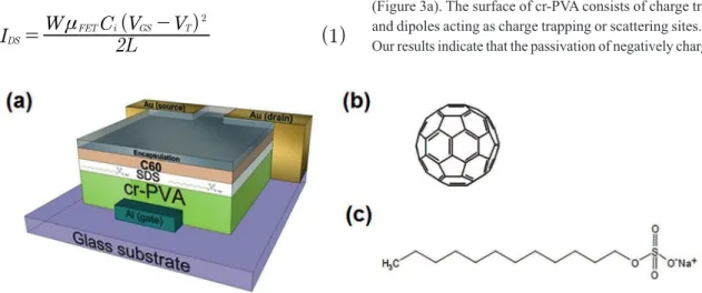
onto glass substrate and PVA was thermally and UV treated to obtain cross-linked PVA (cr-PVA) after which Al layer was covered by spin-coating cr-PVA on top of it. SDS (supplied by Sigma-Aldrich, ACS Reagent > 99%) was dissolved in water at a concentration of 3.0 mg/mL and stirred for one hour at 60°C. A ~20 nm SDS layer was then spin-coated on the Al/cr-PVA ilms at 1500 rpm for 60 s and sequentially annealed in vacuum for 30 min at 100°C followed by C60(Sigma-Aldrich, 99.5%) layer
deposition. C60 was thermally evaporated using shadow mask to
control the layer geometry. Shadow mask patterned gold was
then evaporated to obtain source and drain terminals. Devices
were then encapsulated using 4.5 mg of PIB (polyisobutene, molecular mass: 850-900 g/mol, density: 0.88 mg/mm3, viscosity:
2.5 × 10⁵ SUS at 21°C, supplied by Polibutenos S.A Indútrias
Químicas) that was dropped onto the device areaand covered
with a 0.1 mm thick glass slice, as detailed reported by Toniolo
et al.22 Transistor structure and chemical structure of C 60 are
shown in Figure 1.
Capacitance measurements were performed in Al/cr-PVA/Au and Al/cr-PVA/SDS/Au sandwich structures using an Agilent 4284-A LCR meter, at a frequency of 1 kHz. Transistor characterization was carried out using a Keithley 2602 dual source meter in air in the dark.
3. Results and Discussions
Charge transport in OFETs is governed by several
mechanisms, including the amount of charge accumulated at
the I/S interface following appliance of a potential between
gate and channel semiconductor. Once drain-source voltage
(VDS) is applied, an electric ield along the x-direction results
in the transport of charge along the channel from source to
drain (Figure 2). The drain-source current (IDS) is expressed in saturation regime (VDS>VT) as:
Figure 1: (a) Schematic structure of the SDS-treated OFET, (b) chemical structure of C60, and; (c) chemical structure of SDS.
(
)
( )
I
L
W
C
V
V
1
2
DS
FET i GS T
2
n
=
-where W is the channel width, μis the ield-efect charge carrier mobility, VGS is the applied gate voltage, VT is the threshold voltage and L is the channel length. Increasing
VGS restricts IDS very close to the I/S interface, essentially reducing the efective channel thickness, and hence the very irst few molecular layers of the interface determine the charge transport properties. The drift-difusion equation allows estimating the minimum efective channel thickness (l0) perpendicular to the I/S interface, along the z-direction,
23
in the efective channel bottleneck. It can be expressed as:
where ε is the channel semiconductor dielectric constant,
k is the Boltzmann constant, T is the absolute temperature, e is the electronic charge and Ci is the gate dielectric speciic capacitance.
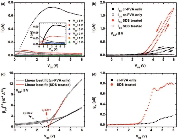
Figure 3a shows the IDS versus VDS plots for the gate voltage VGS varying between 0 and 5 V measured in samples with and without SDS-treated cr-PVA, for comparison. Similar to the behavior observed in conventional FETs with
increasing VDS, the IDS initially increases linearly, then levels
of gradually, and approaches a saturated value. The IDS value is improved when cr-PVA layer is treated with SDS. One important aspect to be kept in mind while working with C60 semiconductor is that, in general the n-type behavior of
organic semiconductor is reasonably sensitive to physically and chemically adsorbed O2 and/or H2O molecules, which can possibly generate electron traps, hence suppressing the charge transport.24-27 In order to protect the device from
the adsorption of O2 or H2O molecules, the C60 layer was
encapsulated using PIB as described above.
The efective channel thickness bottleneck limits the
charge transport because of the presence of charge traps or
dipoles at the I/S interface owing to the surface of the gate
dielectric.28 This is then relected in the form of low μFETand hence low IDS as seen in the output characteristics, IDS(VDS) (Figure 3a). The surface of cr-PVA consists of charge traps
and dipoles acting as charge trapping or scattering sites.15,16
Our results indicate that the passivation of negatively charged
(
)
( )
l
eC V
V
kT
4
2
i GS T
0
=
f
-Figure 2: Schematic representation of FET showing the variation of
efective channel thickness l along the x-direction, with the efective channel represented in gray.
Figure 3: (a) Output characteristics (IDS(VDS)) of SDS treated device (inset shows IDS(VDS) of untreated device) (open circles correspond to IGS(VDS)); (b) transfer characteristics (IDS(VGS)); (c) linear best-it plots for mobility and VT calculation (the curves are taken in the increasing VGS regime), and; (d) transconductance (gm) as a function of VGS, for untreated and SDS treated devices.
[ ( ) /
]
( )
WC
L
d I
dV
2
/3
FET
i
DS GS
1 2 2
n
=
centers on the cr-PVA surface results in enhancement of charge accumulation at the I/S interface, resulting in an increase in
Ci, μFET, IDS (Figure 3a) and transconductance, gm ≡ dIDS/dVGS (Figure 3d). This seems to be contradictory to the observed
displacement of VT to a more positive value (Table 1). But as can be observed in Figure 3c, the slope of the curve
depends on the VGS range, as a consequence implying in a
large uncertainty in the VT value. For this same reason, the
use of the transfer characteristics, IDS(VGS) (Figure 3b) and linear best-it plot for mobility (Figure 3c) also depends on
the VGS interval, despite indicating a clear trend to higher
mobility. It can clearly be seen that the deposition of SDS on top of the cr-PVA layer results in signiicant device
parameters enhancement. SDS is assumed to be working
as a part of the dielectric layer, as an extension of the gate dielectric, since when compared to the untreated devices,
no increase in the OFF current of the SDS-treated ones is observed. Device parameters of both untreated and SDS-treated transistors are summarized in Table 1.
The Dependence of μFET on VGS and on l0 can be determined in saturation regime (VDS> VT) (Figure 4) using
29
which gives direct information about the variation of
mobility with respect to the diferent bottleneck thicknesses
induced by VGS. One important feature observed in the μFET vs.l0 plot (Figure 4b) is that, apart from the magnitude of IDS being higher, the shape of the curve is diferent. It can be seen in Figure 4a that μFET initially increases with increasing VGS,
however, at VGS-VT ≈ 2.3 V (untreated transistor) and VGS-VT ≈ 1.15 V (SDS-treated transistor), a decreasing μFET trend is
observed, which can be attributed to the presence of charged
defects present on the surface of cr-PVA. These charged
defects in principle act as static charges forming energy
Table 1: Device performance parameters for untreated and SDS treated C60-based n-type FETs. The gmand gm/W values were calculated at VDS = 6 V.
Device VT μ (cm2V-1 s-1) C
i (nF cm
-2) I
on/Iof gm (μS)
gm/W
(S cm-1)
cr-PVA only 2.76±0.30 0.18±0.15 15.18 70 0.17 8.50 × 10⁻⁷
SDS treated 2.96±0.10 1.05±0.08 25.38 565 0.81 4.05 × 10⁻⁶
Figure 4: Field efect charge carrier mobility as a function of: (a) VGS-VT, (b) minimum efective channel bottleneck thickness (l0), for
untreated and SDS treated transistors. In both cases VDS = 5 V.
( ) [ ( )]
{ [ ( )]}
exp
exp
l z dz l 1 dz
1 1
FET
l l
z
l
l
01
0 0 0
1 0
0 0
0 0 0
n n n
n
= = - - =
- -
-m m
m
-
#
-#
(4)values correspond to lower l0 (Figure 4b). At lower VGS, the
low of charges is distributed more equally in the channel layer, to a great extent far from the I/S interface. Hence, there is limited interaction of charge carriers with the I/S
interface charged defects, whereas, with increasing VGS, the
low of charge carriers occurs very near to the interface in the channel bottleneck, being hindered by these charge defects originated electrostatic potential variations. The transistor in which the cr-PVA layer is treated with SDS exhibits low
of charge carriers at higher mobility values throughout the
bottleneck (Figure 4b), which is attributed to a lower density of charged defects at I/S interface and the highest μFET value (1.05 cm2 V-1 s-1) is observed at around l
0 = 9 nm.
Sworakowski and co-workers used a mobility dependence
on the distance z to the interface given by the function μ ∝ [1 - exp(-z/λ)] (where λ is a constant of the order of
the molecular dimensions) to account for the interface
neighborhood imposed mobility decay.30,31 The variation in
the average mobility with respect to l0, when the efective
channel bottleneck reaches its minimum thickness (|VGS-VT| → ∞) can then be described using:
where μ0 is the bulk mobility. It is important to keep in mind the limitations of this model, since around 30
nm, the effective channel thickness reaches full thickness
of the C60 layer near to the drain electrode (at low VGS),
hence the further decrease in mobility for larger l0 is witnessed.
Previous reports on C60-based OFETs have usually
stressed on enhancing device performance by improving the metal contact/channel interface by reducing the contact
resistance using several techniques.32,33 Quite recently Du
et al. demonstrated that μFET of C60-based transistors can be
improved by modifying the I/S interface properties. In their work they achieved a highest μFETof 0.31 cm
2 V-1s-1.34 In
top-contact FETs, there are typically two forms of resistances:
metal contact/channel interface resistance and the organic
channel resistance itself. Contact resistance can be reduced by tuning the injection barrier, whereas, for C60-based OFETs
very few studies are found dealing with the reduction of the channel resistance through the improvement of the transport
in the vicinity of the I/S interface. Our work was aimed to minimize the efect of charged defects present on I/S interface
and to enhance the properties of this region to obtain an overall
enhanced OFET performance. After SDS treatment a better charge transport in the channel close to the I/S interface is
observed, hence resulting in a ca.5-fold increase in μFET and
gm and additionally, a ca.8-fold increase in Ion/Iof.
4. Conclusions
In summary, this work was concerned with the development of C60-fullerene based n-channel OFETs with
was not found to be up to the mark when compared with previous reports on C60-based OFETs. Hence in the quest
of improving overall performance, a cost-efective but eicient method was applied, involving deposition of an additional layer of sodium dodecyl sulfate (SDS) anionic surfactant on top of the gate dielectric. The SDS acted as
a treating agent, passivating the positively charged defects
present on the surface of cr-PVA. Field-efect mobility μFET was analyzed as a function of channel bottleneck thickness
and an increase in μFET was observed after SDS treatment.
SDS acted as a part of cr-PVA, signiicantly improving the speciic capacitance and crucial parameters including μFET, gm and on/of current ratio.
5. Acknowledgements
The authors would like to thank CNPq and CAPES for
research grants and fellowships.
6. References
1. Newman CR, Frisbie CD, da Silva Filho DA, Brédas JL, Ewbank PC, Mann KR. Introduction to Organic Thin Film Transistors and Design of n-Channel Organic Semiconductors. Chemistry
of Materials. 2004;16(23):4436-4451.
2. Wöbkenberg PH, Bradley DDC, Kronholm D, Hummelen JC, de Leeuw DM, Cölle M, et al. High mobility n-channel organic ield-efect transistors based on soluble C60 and C70 fullerene
derivatives. Synthetic Metals.2008;158(11):468-472.
3. Li H, Tee BCK, Cha JJ, Cui Y, Chung JW, Lee SY, et al. High-Mobility Field-Efect Transistors from Large-Area Solution-Grown Aligned C60 Single Crystals. Journal of the American
Chemical Society. 2012;134(5):2760-2765.
4. Kao CC, Lin P, Lee CC, Wang YK, Ho JC, Shen YY. High-performance bottom-contact devices based on an air-stable n-type organic semiconductor N, N-bis
(4-triluoromethoxybenzyl)-1,4,5,8-naphthalene-tetracarboxylic di-imide. Applied Physics
Letters.2007;90(21):212101.
5. Wang SD, Minari T, Miyadera T, Tsukagoshi K, Aoyagi Y.
Contact-metal dependent current injection in pentacene thin-ilm transistors. Applied Physics Letters.2007;91(20):203508.
6. Zhou J, Niu QL. Properties of C60 thin ilm transistor based on
polystyrene. Chinese Physics B. 2010;19(7):077305. 7. Anthopoulos TD, Singh B, Marjanovic N, Sariciftci NS, Ramil
AM, Sitter H, et al. High performance n-channel organic
ield-efect transistors and ring oscillators based on C60 fullerene
ilms. Applied Physics Letters.2006;89(21):213504.
8. Cai X, Yu J, Zhou J, Yu X, Jiang Y. Mobility Improvement in C60-Based Field-Efect Transistors Using LiF/Ag Source/
Drain Electrodes. Japanese Journal of Applied Physics.
2011;50(12R):124203.
9. Zhang XH, Domercq B, Kippelen B. High-performance and
electrically stable C60 organic ield-efect transistors. Applied
Physics Letters.2007;91(9):092114.
10. Itaka K, Yamashiro M, Yamaguchi J, Haemori M, Yaginuma S,
Matsumoto Y, et al. High-Mobility C60 Field-Efect Transistors
Fabricated on Molecular- Wetting Controlled Substrates.
Advanced Materials. 2006;18(13):1713-1716.
11. Kitamura M, Kuzumoto Y, Kamura M, Aomori S, Arakawa Y.
High-performance fullerene C60 thin-ilm transistors operating
at low voltages. Applied Physics Letters.2007;91(18):183514.
12. Machado WS, Hümmelgen IA. Low-Voltage Poly(3-Hexylthiophene)/
Poly(Vinyl Alcohol) Field-Efect Transistor and Inverter. IEEE
Transactions on Electron Devices. 2012;59(5):1529-1533.
13. Machado WS, Hümmelgen IA. Low voltage organic ield efect transistors with a poly(hexylthiophene)–ZnO nanoparticles
composite as channel material. Physica Status Solidi (RRL) -
Rapid Research Letters. 2012;6(2):74-76.
14. van Etten EA, Ximenes ES, Tarasconi LT, Garcia ITS, Forte MMC,
Boudinov H. Insulating characteristics of polyvinyl alcohol for integrated electronics. Thin Solid Films. 2014;568:111-116.
15. Lee CA, Park DW, Jin SH, Park IH, Lee JD, Park BG. Hysteresis
mechanism and reduction method in the bottom-contact pentacene
thin-ilm transistors with cross-linked poly(vinyl alcohol) gate
insulator. Applied Physics Letters.2006;88(25):252102.
16. Hyung GW, Lee DH, Koo JR, Kim YK, Park J. Organic ield-efect transistors with surface modiication by using a PVK bufer layer on lexible substrates. Journal of the Korean
Physical Society. 2012;61(10):1720-1723.
17. Cruz-Cruz I, Tavares ACB, Reyes-Reyes M, López-Sandoval R, Hümmelgen IA. Interfacial insertion of a poly (3, 4-ethylenedioxythiophene): poly (styrenesulfonate) layer between the poly (3-hexyl thiophene) semiconductor and cross-linked poly (vinyl alcohol) insulator layer in organic ield-efect transistors. Journal of Physics D: Applied Physics.
2014;47(7):075102.
18. Nawaz A, Cruz-Cruz I, Rodrigues R, Hümmelgen IA. Performance enhancement of poly (3-hexylthiophene-2, 5-diyl) based ield efect transistors through surfactant treatment of the poly (vinyl alcohol) gate insulator surface. Physical Chemistry Chemical
Physics.2015;17(40):26530-26534.
19. de Col C, Nawaz A, Cruz-Cruz I, Kumar A, Kumar A, Hümmelgen IA. Poly(vinyl alcohol) gate dielectric surface treatment with vitamin C for poly(3-hexylthiophene-2,5-diyl) based ield efect
transistors performance Improvement. Organic Electronics. 2015;17:22-27.
20. Jastrombek D, Tavares ACB, Meruvia MS, Koehler M, Hümmelgen IA. Improved charge carrier mobility in copper phthalocyanine based ield efect transistors by insertion of a
thin poorly conducting layer as gate insulator extension. Physica
Status Solidi (A). 2015;212(12):2759-2765.
21. Jastrombek D, Nawaz A, Koehler M, Meruvia MS, Hümmelgen IA. Modiication of the charge transport properties of the copper phthalocyanine/poly(vinyl alcohol) interface using cationic or anionic surfactant for ield-efect transistor performance enhancement.
Journal of Physics D: Applied Physics. 2015;48(33):335104.
22. Toniolo R, Hümmelgen IA. Simple and Fast Organic Device Encapsulation Using Polyisobutene. Macromolecular Materials
23. Seidel KF, Koehler M. Modiied Lampert triangle in an
organic ield efect transistor with traps. Physical Review B.
2008;78(23):235308.
24. Matsuoka Y, Inami N, Shikoh E, Fujiwara A. Transport properties of C60 thin ilm FETs with a channel of several-hundred
nanometers. Science and Technology of Advanced Materials.
2005;6(5):427-430.
25. Hamed A, Sun YY, Tao YK, Meng RL, Hor PH. Efects of oxygen and illumination on the in situ conductivity of C60 thin
ilms. Physical Review B. 1993;47(16):10873.
26. Pevzner B, Hebard AF, Dresselhaus MS. Role of molecular oxygen and other impurities in the electrical transportand dielectric
properties of C60 ilms. Physical Review B. 1997;55(24):16439.
27. Könenkamp R, Priebe G, Pietzak B. Carrier mobilities and inluence
of oxygen in C60 ilms. Physical Review B. 1999;60(16):11804.
28. Benvenho ARV, Machado WS, Cruz-Cruz I, Hümmelgen IA. Study of poly(3-hexylthiophene)/cross-linked poly(vinyl alcohol) as semiconductor/insulator for application in low voltage organic ield efect transistors. Journal of Applied
Physics.2013;113(21):214509.
29. Shea PB, Kanicki J, Ono N. Field-efect mobility of polycrystalline tetrabenzoporphyrin thin-ilm transistors. Journal of Applied
Physics. 2005;98(1):014503.
30. Sworakowski J, Bielecka U, Lutsyk P, Janus K. Efect of spatial inhomogeneity of charge carrier mobility on current–voltage characteristics in organic ield-efect transistors. Thin Solid
Films. 2014;571(Part 1):56-61.
31. Sworakowski J. Current–voltage characteristics in organic ield-efect transistors. Efect of interface dipoles. Chemical
Physics. 2015;456:106-110.
32. Kubozono Y, Haas S, Kalb WL, Joris P, Meng F, Fujiwara A, et al. High-performance C60 thin-ilm ield-efect transistors with
parylene gate insulator. Applied Physics Letters.2008;93(3):033316.
33. Zhang XH, Kippelen B. High-performance C60n-channel organic
ield-efect transistors through optimization of interfaces Journal
of Applied Physics. 2008;104(10):104504.
34. Du L, Luo X, Wen Z, Zhang J, Sun L, Lv W, et al. A striking
performance improvement of fullerene n-channel ield-efect transistors via synergistic interfacial modiications. Journal