Abstract— In this paper a novel design of microstrip diplexer and triplexer using open loop resonators is presented. The proposed diplexer if formed by two band-pass filters for the Industrial Scientific Medical (ISM) applications at 5.8 GHz and the WIMAX applications (IEEE 802.16 WiMAX at 3.17 GHz to 4.2 GHz bands). The microstrip triplexer is designed for the Digital Communication System (DCS) at 1.8 GHz, WIMAX at 3.2 GHz and for the C-band at 4.4 GHz. Each device is formed by a set of filters with a matching network by using open loop resonators and a good arrangement of the transmission feed lines. Several parametric studies were achieved to study the influence of some critical parameters on the performances of the proposed circuits. The LC equivalent circuit of the band pass filter is examined and the values of its components are calculated. ADS Agilent and CST-MWS solvers are used to predict the electrical performances of the proposed circuits. The simulated frequency responses of these structures show good results with insertion losses around 2 dB, return losses better than 20 dB for all channels, and an isolation between all bands better than 20 dB. Besides, several transmission zeros are observed near the pass bands which enhance the selectivity and the isolation of the proposed devices.
Index Terms— Band pass filter, diplexer, open-loop resonators, selectivity, transmission zeros, triplexer.
I. INTRODUCTION
With the rapid development of the telecommunication system industry, especially the expansion of
portable devices, designers are in the pursuit of new technologies and topologies to miniaturize the
electronic components and to attain better electrical performances.
In order to miniaturize an electronic component, using a single antenna represents a good alternative
to reduce the volume and the mass of the whole device. In this context, multiplexers and diplexers are
key components in many microwave communication systems, such as radar systems, cellular phones,
and satellite communication systems.
Multiplexer is a passive multiport device formed by a set of filters and a common junction. The
main role of this device is to combine or to separate signals that have different frequency bands.
Design of a Microstrip Diplexer and Triplexer
Using Open Loop Resonators
A. Chinig, A. Errkik, L .El Abdellaoui, A. Tajmouati
LMEET Laboratory, FST of Settat Hassan 1stUniversity – Morocco
J. Zbitou,
LMEET Laboratory, FPK/FST of Settat Hassan 1stUniversity – Morocco
M. Latrach
While the diplexer represents the simplest form of a multiplexer. It allows a simultaneous
transmission and reception of signals by using a single antenna. [1]
The development and the proliferation of standards, has led to the emergence of various innovations
in diplexers/multiplexers technologies. Therefore, multi-services and multi-bands communication
systems are searching new multiplexers and diplexers with high performances, low losses, high
isolation, low cost and small size.
In the past, several technologies have been proposed in the literature to realize microwave
components. Microwave devices particularly, filters, diplexers and multiplexers using waveguides and
dielectric resonators are widely used for their high performances and the high power they can handle
[2]-[3]-[4]-[5]-[6]-[7]. However, they are too heavy and bulky and their fabrication processes are too
expensive.
Among all technologies used to design and to realize RF filters, microstrip technology remains the
most popular due to its ease of integration with other electronic components and its compatibility with
the planar fabrication process. Furthermore, this technology favors the miniaturization, since it is
light, occupies a small size, and it is less expensive. Many contributions in this research area have
been introduced, and several design approach have been proposed [8]-[9]-[10]-[11]-[12]. However,
the main disadvantage of the microstrip technology is the low quality factor usually obtained.
In this paper, a new topology of microstrip diplexer and triplexer is proposed based on the open
loop resonators. A brief study on the open loop resonator is carried to investigate the resonant
frequencies and the transmission zeros of this kind of resonators by using the even and the odd-mode
analysis method. Based on the open loop resonator and a good arrangement of the transmission feed
lines, a band pass filter is then designed and simulated to operate at the 5.8 GHz. This microstrip
structure is converted to its LC equivalent model based on a detailed method discussed in this work.
After the design of this microstrip BPF another filter is designed to operate at 3.2 GHz and combined
with the first one to form the proposed microstrip diplexer. Several parametric studies were achieved
to examine the influence of some critic parameters on the behavior of the proposed band pass filter
and the diplexer. Finally, and according to the same method used to design the microstrip diplexer, a
microstrip triplexer is then designed to operate at 1.8GHz, 3.2 GHz and 4.4 GHz respectively.
II. OPEN LOOP RESONATORS
The microstrip open loop resonator is one of the most utilized topologies to design filters diplexers
mixers and antennas [13]. Known also under the name of the U-shaped resonator, this type of
structure is just a folded transmission line resonator with a gap in one of its sides as shown in Fig. 1.a.
Due to its numerous advantages including compact size and versatility, great number of microwave
components using open loop resonators have been widely reported [14]-[15]-[16]-[17]. However, the
main disadvantage of this kind of resonators is the presence of high order of harmonic, which limits
A. Resonant Frequencies
The main objective of this section is to study the resonance modes of the open loop resonator and
its applications in the design of the microwave band pass filters.
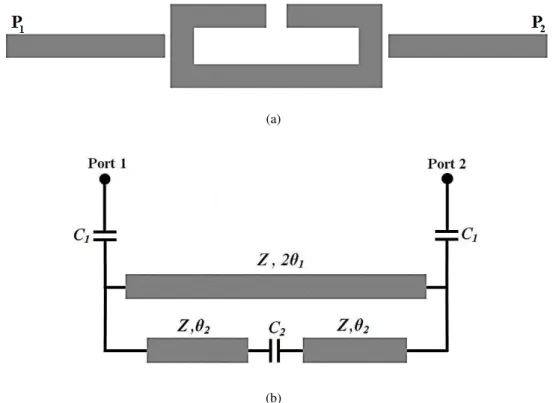
Fig. 1.a represents the proposed open loop resonator. This conventional resonator is obtained by
folding a straight-line resonator characterized by a total electrical length θT and an impedance
characteristic Z. Since the structure is symmetric, it can support the even and the odd modes. Based
on a previous work [18], it was proved that the behavior of the open loop resonator can be deduced by
analogy to that of the straight-line resonator. The resonance occurs when T nin other terms when
the length of this resonator is multiple of λ/2 where the λ is the wavelength andT l. In this work,
in order to derive the resonant frequencies of the open loop resonator, the even and the odd-mode
analysis method is used. It can be noticed also that the presence of the end-coupled arms of the open
loop resonators increase the load capacitance and create tunable transmission zeros [19].
(a)
(b)
Fig. 1. (a) Schematic of the open loop resonator (b) The equivalent transmission line model.
First, the Fig. 1.b gives the equivalent transmission line model of the open loop resonator. The Fig.
2 shows the even-mode and the odd-mode equivalent transmission line model. C1 is used to model the
coupling capacitance between the resonator and the input/output ports. The coupling between the two
transmission lines of the resonator is modeled by the capacitance C2. Since the line width of the
proposed resonator is constant the characteristic impedance is uniform, thus the open loop resonator
can be modeled by two transmission line with the same characteristic impedance Z and two different
(a) (b)
Fig. 2. (a) The odd-mode equivalent circuit (b) The even-mode equivalent circuit.
In this analysis approach, the resonant frequency f0 denote the first resonant frequency in the
odd-mode while f1 represents the first resonant frequency in the even-mode. Based on the even and the odd
mode equivalent models, the odd mode input admittance can be given by:
1 2 2 1 2 2
2 2 2 2 1 1
2 tan cot 2 tan 1
2 tan 2 tan 1 cot
o in
C C Z C Z
Y j
C Z C Z C Z
(1)
The resonance occurs when
Yino 0 (2)
Otherwise, for a given value of C2, Z, θ1, and θ2 the resonant frequencies can be obtained by the
following expression:
2C Z2 tan2
cot 1
2 C Z2 tan2 1
0 (3)In the same way, the input admittance for the even mode can be determined as follow:
11 1 2 21
tan tan tan tan e in C Y j C Z
(4)
Similarly, the resonant condition for the proposed structure in the even mode is expressed as
follow:
tan1tan2 0 (5)
It is known that the transmission zeros appears near the pass band when the parameter S21=0. The
even and the odd mode analysis can give the expression of the S21 based on the odd- and the
even-mode input admittances. The expression of the S21 is given by:
21
o o e o in in o o e o in in
Y Y Y Y
S
Y Y Y Y
(6)
Where Yo represents the characteristic admittance. The condition that ensures the appearance of the
transmission zeros can be deduced from the equation (6). Thus, we can write:
In other words, this condition can be expressed as fellow:
Z C 2
sin 21sin 22
cos22 0 (8)B. LC model of the proposed open loop band pass filter
The design approach of the microstrip diplexer begins generally by the design of two band pass
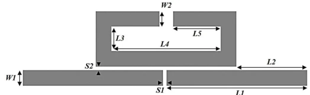
filters. The Fig. 3 presents the proposed topology of the microstrip band-pass filter. As can be clearly
seen this structure consists of a conventional rectangular open loop resonator and two Input/output
feed lines. The coupling between the two transmission lines and the resonator is achieved by the gap
S2 while the gap S1 separates the two feed lines. In this case, the folded microstrip resonator and the
good arrangement of the two feed lines ensure a better reduction in size.
Fig. 3. The proposed band pass filter based on open loop resonator.
The dimensions of the proposed band pass filter using open loop resonator are: W1=0.75, W2=0.75,
S1=0.2, S2=0.2, L1=7, L2=3.6, L3=1.25, L4=5.5, L5=2.4, all in (mm).
Fig. 4. Simulation results of the proposed band pass filter.
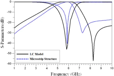
To investigate the operation of the proposed band pass filter, the designed circuit is simulated using
the EM simulator ADS Agilent. From the Fig. 4 it can be seen that the band pass filter has a center
frequency at 5.8 GHz, a fractional bandwidth of 19.6 %, a return loss of 24 dB, and an insertion loss
of 1.26 dB. Moreover, the band pass filter presents a transmission zero near the pass band edge
located at 7.28 GHz with an attenuation of 26.6 dB.
In order to understand the behavior of the proposed band pass filter, a second approach of this work
is dedicated to study this topology by converting the microstrip structure to its equivalent LC model
Since the proposed structure is symmetric, converting the microstrip transmission lines to the LC
model is easy by using the half circuit LC analysis. The equivalent LC model is approximate and the
microstrip transmission lines are considered lossless. In this LC model, the parameters L1, L2, L3, L4,
L5, L6, L7, L8, and L9 represent the inductances of central transmission lines; C1 is used to model the
capacitance effect of the gap between the two feed lines while C2 and C3 represent the capacitance
effects of the gap between the feed line and the resonator. C8 and C9 represent the capacitance effects
of the open stubs with respect to the ground. Furthermore, the parameters C3, C4, C5 and C6 represent
the capacitance effects of the bends.
After dividing the microstrip structure to small parts in order to facilitate the conversion process,
every part of the microstrip line is then converted to its equivalent LC component. The calculation
method described in the following section is used to obtain the electrical values of each component.
Finally, and for a better matching between the simulations results of the two circuits, some tuning
techniques are employed.
To calculate the values of each component in the LC model, the equations (9) and (10) are used.
lCZ vc p (9)
p
c Lv l
Z
(10)
Parameters l, C and L represent the length, the capacitance and the inductance of a microstrip line,
if the line width is considered constant. Zc is the characteristic impedance and vp represents the phase
velocity.
However, calculating the C and L values needs the calculation of Zc and vp. Once the effective
dielectric constant εre is determined, the phase velocity is given by:
p re c v
(11)
c represents the velocity of light in free space.
The effective dielectric constant εre and the characteristic impedance Zc can be determined by the following equations:
For W/h1
0.5 2
1 1
1 12 0.04 1
2 2 r r re h W W h
(12)
ln 8 0.25 2 c re h W Z W h
(13)
For W/h1
0.5 1 1 1 12 2 2 r r re h W
1
1.393 0.677ln 1.444
c re
h W
Z
W h
(15)
Where w is the width of the microstrip line, h and εr represent the thickness and the permittivity of
the substrate, εre is the effective permittivity, the parameter η = 120π Ω is the wave impedance in free space.
Each right angle bend in the microstrip open loop resonator can be modeled by an equivalent T-
network as described in [20]. In this work, an approximate form to evaluate the capacitance can be
given by the expressions (16) and (17).
( / ) (14 12.5) / (1.83 2.25) 0.02 / /
r W h r r
C
pF m
W W h W h
for W h/ 1 (16)
C (pF m/ ) (9.5 r 1.25)W h/ 5.2 r 7
W for W /h1 (17)
Fig. 5. The LC model of the proposed band pass filter.
The two primordial parameters that should be calculated are the effective dielectric constant and the
characteristic impedance, thus for a line width equal to 0.75 mm we obtain (εre=3.05, Zc=97.7 Ω). After the application of the calculation method, the next step is the simulation of the converted circuit
in a schematic environment. In order to get a better matching between the simulations results of the
EM and the converted circuit, several simulations were achieved by tuning the obtained values of
each LC model component. The EM simulator ADS was used to simulate and to compare the
simulated results of the two circuits in the same frequency range. Fig. 6 demonstrates the simulated
results of the LC model and the microstrip band pass filter. As seen in the figure, it can be observed
that there is a good agreement between the two frequency responses. The final values of the LC
components used in circuit simulation are as follow:
L1= 3.85, L2= 1.5, L3=0.7, L4=1.3, L5= 0.12, L6=3.85, L7=1.5, L8= 0.7 and L9= 1.3 (all in nH).
C1=0.05, C2=0.15, C3=0.15, C4=0.032, C5=0.032, C6=0.032, C7=0.032, C8=0.14, C9=0.14, C10=0.015
Fig. 6. Simulated results of the LC model and the Microstrip band pass filter.
One of the essential studies to understand the behavior of the proposed band pass filter is to vary the
dimensions of some geometric parameters of the proposed structure, which represents an interesting
way to optimize the performance of the filter.
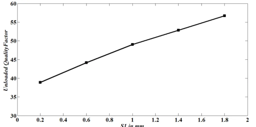
The gap S1 between the two feed lines was found to be a critical design parameter. In this context,
various simulations were achieved to examine the frequency responses of the filter under different
values of the gap S1.
Fig. 7. The simulated S21 parameter for different values of the gap S1.
Fig. 7 represents the simulation results of the parameter S21 for different gap widths. From the Fig.
7, two effects can be observed. The first is related to the bandwidth. When the gap increases, a smaller
bandwidth is observed with a slight increase in the insertion losses. This is can be attributed to the
reduction of the periphery between the feed lines and the resonator. In other hand, varying the gap
width can affect the location and the attenuation of the transmission zero. As can be seen, when the
gap width is increased the location and the attenuation of the transmission zero increase, thus
signifying a better selectivity. The presence of this transmission zero is a result of the cross coupling
between the two end coupled arms of the resonator as well as between the two input/output lines.
Varying the gap alter also the return loss of the filter. To have a clear idea on the insertion loss of
the band pass filter and its selectivity, the unloaded quality factor Q0 of the band pass filter calculated
from the equation (19), can envisage a measure of its electrical performances [21].
0 3
0 1
2 1 ( )
L
dB
e
f Q
f
Q Q
(18)
0 /20
(1 10 )
L L Q
Q
(19)
with f0 is the resonant frequency, (Δf)3dB is the – 3 dB bandwidth of the pass band, L is the insertion
loss in decibel and QL is the loaded Q obtained by the equation (18). Qe is the external quality factor.
Fig. 8. The evolution of the simulated unloaded quality factor for different values of the gap S1.
From the Fig. 8, it can be observed that the unloaded quality factor increases when the gap between
the two feed lines increases. When the gap width increases from 0.2 mm to 1.8 mm, the overall size of
the filter increases and that generates an increase in the radiation loss and a decrease in conduction
loss. So, these results can be attributed to the decrease of the current density which leads to a high
unloaded quality factor [21].
III. DESIGN OF MICROSTRIP DIPLEXER.
Based on the open loop resonator shown in Fig. 3, and according to the position of the microstrip
feed lines, it was proved that this kind of structure can be applied to design a band pass filter
operating at 5.8 GHz. Similarly, another band pass filter operating at 3.2 GHz was designed using the
FR4 substrate with a thickness of 1.6 mm, a relative electric constant of 4.4, a loss tangent of 0.025
and a conductor thickness of 35 um. The size of the proposed diplexer is extremely small, with an
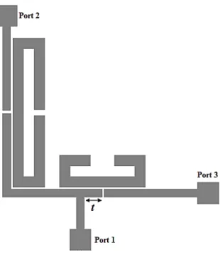
Fig. 9. Layout of the proposed microstrip diplexer.
The classical approach to design a diplexer starts with the design of two band pass filters operating
at different pass bands. After that, it is essential to combine them with a matching network. This part
of the circuit is so important in the design procedure, since combining the two band pass filters
engenders generally a degradation in the diplexer performances. The solution used in this work
involves keeping the dimensions of the junction constant during the design of each band pass filter.
When, it comes to combine the two BPFs, a careful adjustment of some geometric parameters is
necessary for the two resonators. The dimensions of the junction and the input/output feed lines
remain unchanged.
The proposed diplexer is shown in Fig. 9. As can be seen this structure consists of a matching
network based on tapped feed line connected to the port 1, two transmission lines representing the
input/output ports, and two open loop resonators tuned to operate at the desired resonant frequencies.
The two resonators allow the passage of the energy to the two input/output feed lines through cross
coupling.
According to the analysis performed on the band pass filter in the first section, it can be concluded
that this kind of resonator has specific performances. This pseudo-elliptic topology presents a
transmission zeros near the pass band that will improve the rejection in the stop band and enhance the
isolation of the proposed diplexer. Moreover, this structure is suitable to design a band pass filter with
a minimum loss in the band pass and a wide bandwidth. Therefore, it is possible to realize a
microstrip diplexer with high rejection level and good electrical performances with a limited filter
Fig. 10. Simulated results of the proposed microstrip diplexer using ADS Aglient.
Fig. 11. Simulated results of the microstrip diplexer using CST-MWS.
The Fig. 10 represents the simulation results of the proposed diplexer. The simulated insertion loss
is about 1.86 dB for the Rx filter and 2 dB for the Tx filter. The return loss in the upper and lower
filter is about 27 dB and 21 dB, respectively. The simulated -3 dB pass bandwidth is about 8.9 % and
9.75 % for the high and the low band respectively. The isolation between the two channels is greater
than 20.8 dB. Moreover, several transmission zeros near the pass bands located at 2.42 GHz, 3.52
GHz, 5 GHz and 7.25 GHz with attenuation of 42.6 dB, 26.9 dB, 48.2 dB and 42.44 dB respectively
are obtained.
It can be noticed that the EM simulator ADS Agilent is a 2D simulator. So in order to verify and to
examine the electrical performances of the proposed microstrip diplexer, the CST-MWS a 3D EM
simulator was utilized to design and to simulate the circuit. The simulation results obtained by this
simulator are depicted in the Fig. 11. The Table I gives a resume and a comparison between the
simulation results obtained by the two different simulators. Obviously, the simulated results with ADS
TABLE I. THE SIMULATION RESULTS OF THE PROPOSED DIPLEXER UNDER DIFFERENT EM SIMULATORS.
It is known that the external quality factor characterize the excitation of the resonators, and it
depend mainly on the filter bandwidth. The external quality factor can be calculated by the equation
(20).
0 0
2 L
e
L Q Q Q
Q Q
(20)
The Fig. 12 shows the simulated external quality factor versus the position of the input feed line
denoted by t (Fig. 9). The position of the input feed line affects the bandwidth and the central
frequency of each band pass filter.
Fig. 12. The evolution of the simulated external quality factor for different values of t.
From the Fig. 12, it can be observed that, when t is adjusted from 1.7 mm to 3.3 mm; the fractional
bandwidth ratio of the upper channel varies from 11.3% to 7.36% while it varies from 10.26% to
9.45% for the lower channel. The variation of the parameter t has a significant impact on the
fractional bandwidth of the Rx band pass filter and a slight influence on the Tx band pass filter. Thus,
an important decrease is observed for the external quality factor of the Rx filter while the external
quality factor of the Tx filter decreases slightly for the same variation of the parameter t.
Parameter Simulation results (ADS) Simulation results (CST)
TX RX TX RX
Frequency GHz 3.2 5.84 3.2 5.9
Bandwidth 312 MHz 515 MHz 405 MHz 657 MHz
Insertion loss dB 1.86 2 1.6 2
TABLE II.A COMPARISON BETWEEN THE PROPOSED DIPLEXER AND OTHER DIPLEXERS.
Center frequency f0 in
GHz
|S12|/|S11| (dB) -3 dB FBW (%) Isolation
in (dB)
Circuit size (mm2)
Stop band range
Average S21
-magnitude of stop band (dB) Tx band Rx band Tx band Rx band Tx band Rx band Microstrip diplexer using open loop resonators
3.2 5.84 1.8/21 2/27 9.75 8.9 21 24×22 Up to 10 GHz
20
Ref[22] 1.5 2 2.7/20 2.8/20 3.4 3.4 40 33.9×54
.4
Up to 8 GHz
20
Ref [23] 1.575 2.45 2.5/18 1.4/18 3 8 40 30×70 Up to
6 GHz
20
Ref [24] 1.95 2.14 1.22/1 5
1.12/1 5
3.1 2.8 30 40×70 Up to 5.6 GHz
30
In order to have a clear idea about the electrical performances of the proposed diplexer, Table II
gives a comparison between the microstrip diplexer using the open loop resonator and other
microstrip diplexers proposed in literature. As it can be seen, the microstrip diplexer based on open
loop resonators presents low insertion loss, wide pass band, and high return loss compared to the other
diplexers. Thus, the proposed circuit presents interesting electrical characteristics. In addition, the
proposed diplexer is characterized by a compact size of 24×22 mm2 and a wide stop band with an
attenuation of 20 dB up to 10 GHz, which allows it to be a very selective diplexer. However,
compared to the other microstrip diplexers, the isolation between the two channel filters should be
enhanced.
IV. DESIGN OF MICROSTRIP TRIPLEXER.
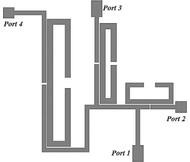
The proposed microstrip triplexer is shown in the Fig. 13. This circuit is formed by connecting
three band pass filters operating at different frequency bands with a matching network.
Conventionally, the triplexer design need three band pass filters. Each filter can be designed
individually to operate at a specific frequency band before combining it with the other channel filters.
The matching network represents the main challenge in the design procedure since this part of the
circuit become more complicated and can influence the frequency response of the circuit. Thus,
designing a triplexer structure is more complicated than the design of the diplexer structure. Similarly,
before combining the three BPFs, the dimensions of the matching network are kept constant during
the design of each filter, which simplifies the design procedure of the triplexer. This method shows its
efficiency since the only parameters that should be adjusted are the geometric parameters of the open
loop resonators.
Based on the diplexer designed in previous section, another BPF operating at 1.8 GHz is designed.
BPFs already designed for the proposed diplexer. The three BPFs operating at 1.8 GHz, 3.1 GHz and
4.4 GHz are denoted channel 1, channel 2 and channel 3 respectively.
Fig. 13. The topology of the microstrip diplexer using open loop resonators.
Fig. 14 shows the simulation results of the microstrip diplexer. From the simulated results obtained
by the EM simulator ADS Agilent, the insertion losses are about 1.97 dB, 1.99 dB, and 2.3 dB for the
cannels 1, 2 and 3 respectively. The return losses are better than 22 dB for the three pass bands. The
fractional bandwidths of each filter are about 7.44%, 7.45%, and 6.23% respectively. Besides, the
isolation between the channels 1 and 2 is better than 21.5 dB, while it is better than 20 dB between the
two channels 1 and 3, concerning the isolation between the channels 2 and 3 it is about 20 dB.
Moreover, each filter presents several transmission zeros located near the pass bands. The prototype
circuit size is around 33×34mm2. Table III resumes the simulated results of the proposed triplexer.
(a) (b)
TABLE III: THE SIMULATION RESULTS OF THE MICROSTRIP TRIPLEXER USING THE ADSAGILENT.
V. CONCLUSION
In this paper, a novel compact microstrip band-pass filter structure has been proposed for designing
diplexer and triplexer. It consists of an open loop resonator coupled to two Input/output feed lines.
The band-pass filter with high electrical performances exhibits a quasi-elliptic function response with
two transmission zeros that improve the selectivity. The derived lumped element circuit of the band
pass filter can give a good estimation of the full-wave simulation response. Thus can simplify the
design of circuits using open loop resonators. The parametric studies performed for the BPF and the
diplexer as well as the simulated results of the proposed band pass filter, the diplexer and the triplexer
have demonstrated an interesting filtering characteristics. These proposed circuits are very attractive
for the ISM, DCS, WIMAX and the C-band applications. Furthermore, these circuits are very
compact with an overall size of 24 × 22 mm2 for the diplexer and 33×34 mm2 for the triplexer.
REFERENCES
[1] Pozar, D. M.: Microwave Engineering. John Wiley & Sons (1998)
[2] T. Gál, J. Ladvánszky, and F. Lénárt. ‘‘Improvement of Waveguide Diplexer Components,’’ IEEE, Asia-Pacific Microwave Conference Proceedings. pp 28-30. 2013.
[3] Enzo Cavalieri d'Oro, Giuseppe Macchiarella ‘‘A High Power Waveguide Diplexer in Ku-band for Satellite Ground Station,’’ IEEE Microwave Conference, 1989. 19th European. pp 1052-1057. 1989.
[4] Skaik, T, Lancaster, M., Maolong Ke., Yi Wang, ‘‘A micromachined WR-3 band waveguide diplexer based on coupled resonator structures,’’ IEEE, Microwave Conference (EuMC), 2011 41st European. pp 770-773. 2011.
[5] Cheng Chen, Liu Chen, Peng Zhao. ‘‘A waveguide diplexer based on E-plane T-junction,’’ 15th IEEE, International Conference on Electronic Packaging Technology (ICEPT), pp 1390-1391. 2014.
[6] Bunin A. V., Vishnyakov S. V., Gevorkyan V. M., Kazantsev J. A., Mikhalin S. N., Polukarov V. I. ‘‘ S, C-Band Dielectric Resonator Diplexer,’’ IEEE, 16th Int. Crimean Conference "Microwave & Telecommunication Technology" (CriMiCo'2006). 11-15 September, Sevastopol, Crimea, Ukraine.
[7] Bunin A.V., Vishnyakov S.V., Gevorkyan V.M., Kazantsev, J.A., Mikhalin, S.N., Polukarov, V.I. ‘‘ KU-band dielectric resonator diplexer,’’ IEEE, 18th International Crimean Conference on Microwave & Telecommunication Technology, CriMiCo 2008. pp 478-479.
[8] Tantiviwat S., Intarawiset N., Jeenawong R. ‘‘Wide-stopband, compact microstrip diplexer with common resonator using stepped-impedance resonators,’’ IEEE, TENCON Spring Conference, pp 174-177, 2013.
[9] Xinwei Chen, Wenmei Zhang, Chunhui Yao. ‘‘Design of Microstrip Diplexer with Wide Band-stop,” IEEE, International Conference on Microwave and Millimeter Wave Technology, ICMMT '07. pp 1-3. 2007.
[10] Chi-Feng Chen, Cheng-Yu Lin, Bo-Hao Tseng, Sheng-Fa Chang. ‘‘High-Isolation and High-Rejection Microstrip Diplexer with Independently Controllable Transmission Zeros,’’ IEEE, Microwave and Wireless Components Letters, Volume: 24. pp 851-853. 2014.
Channel 1 Channel 2 Channel 3
Frequency GHz 1.8 3.1 4.46
Bandwidth 134 MHz 231 MHz 278 MHz
Insertion loss dB 1.97 1.99 2.3
[11] Qi Zhang, Xueguan Liu, Huiping Guo, Ying Wang. ‘‘A novel compact diplexer based on folding microstrip lines,’’ IEEE, 4th International Symposium on Microwave, Antenna, Propagation, and EMC Technologies for Wireless Communications (MAPE), 2011. pp 785 - 788.
[12] Seungpyo Hong, Kai Chang. ‘‘Stub-tuned Microstrip band Pass Filters for Millimeter-wave Diplexer Design,’’ IEEE, Microwave and Wireless Components Letters, 2005. volume 15, pp 582-584.
[13] K. Chang and L.H. Hsieh, Microwave Ring Circuits and Related Structures, 2nd Edition. John Wiley & Sons, New Jersey, 2004.
[14] Jia-Sheng Hong., Lancaster, M.J. ‘‘Theory and experiment of novel microstrip slow-wave open-loop resonator filters,” IEEE Transactions on Microwave Theory and Techniques, 1997. vol. 45, no. 12, pp. 2358–2365..
[15] Jia-Sheng Hong, Lancaster, M.J. ‘‘Aperture-coupled microstrip open-loop resonators and their applications to the design of novel microstrip band-pass filters,’’ IEEE Transactions on Microwave Theory and Techniques, 1999. vol. 47, no. 9, pp. 1848–1855.
[16] Cheng-Cheh Yu, Kai Chang. ‘‘Novel compact elliptic-function narrow-band band pass filters using microstrip open-loop resonators with coupled and crossing lines,’’ IEEE Transactions on Microwave Theory and Techniques, 1998. vol. 46, no. 7, pp. 952–958.
[17] Konpang, J., Thongnoi, L. ‘‘A Compact Four-pole Cross-coupled Square Open Loop Resonator Diplexer,’’ IEEE, German Microwave Conference (GeMIC), 2011. pp 1-4.
[18] A.Chinig, J. Zbitou, A. Errkik, L. Elabdellaoui, A. Tajmouati, A. Tribak, M.Latrach. ‘‘A New Microstrip Diplexer Using Open-Loop Resonators,’’ Journal of Microwaves, Optoelectronics and Electromagnetic Applications, vol. 13, No. 2, pp 75-86. December 2014.
[19] K. S. Chin, D.J. Chen. ‘‘Novel Microstrip Bandpass Filters Using Direct-Coupled Triangular Stepped Impedance Resonators for Spurious Suppression,’’ Progress In Electromagnetics Research Letters, 2009. vol. 12, pp 11-20.
[20] J-S. Hong, Microstrip Filters for RF/Microwave Application, 2nd ed. (Wiley, New York, 2011).
[21] Jarry, P., Beneat, J. Design and Realizations of Miniaturized Fractal RF and Microwave filter, A John Wiley & Sons, Inc., Publication. (2009).
[22] Chen, C. F., Huang, T. Y., Chou, C. P., & Wu, R. B. ‘‘Microstrip diplexers design with common resonator sections for compact size, but high isolation,’’ Transactions on Microwave Theory and Techniques, IEEE, 2006. pp 1945-1952.
[23] Huang, C. Y., Weng, M. H., Ye, C. S., & Xu, Y. X. ‘‘A high band isolation and wide stopband diplexer using dual-mode stepped-impedance resonators,’’ Progress In Electromagnetics Research, 2010. 100, pp 299-308.