Efficiency Enhancement in Polycrystalline CdS/CdTe Solar Cell via Diffraction
Grating and Engineering Absorber and Back Surface Field Layers
M. MAHOODI
Department of Electrical Engineering, Ferdowsi University of Mashhad, Mashhad 9177948974, Iran malihe.mahoodi@mail.um.ac.ir Received 27/08/2018 – Accepted 16/11/2018 DOI: 10.15628/holos.2018.7668 ABSTRACT
In this paper, the effect of diffraction grating and engineering absorber and back surface field (BSF) layers on performance of a single-‐junction polycrystalline cadmium sulfide/cadmium telluride (CdS/CdTe) solar cell have investigated. At first, the electrical characteristics of reference CdS/CdTe solar cell is simulated and validated with experimental data of fabricated CdS/CdTe solar cell. In order to improve the maximum efficiency, a new structure with diffraction grating and engineering absorber and back surface field layers is presented. Furthermore, the effect of carrier
lifetime variation in the absorber layer on the conversion efficiency of solar cell was investigated. It is found that diffraction grating and engineering absorber and back surface field layers can increase the conversion efficiency of the solar cell by about 1.02% and 6% compared with reference cell, respectively. Under global AM 1.5 conditions, the open circuit voltage, short circuit current density, fill factor and conversion efficiency of optimized solar cell structure are 1114 mV, 25.35 mA/cm2, 0.8856 and 25.022%, respectively.
KEYWORDS: Cadmium sulfide/cadmium telluride, polycrystalline CdS/CdTe solar cell, conversion efficiency,
diffraction grating, engineering absorber and back surface field layers, carrier lifetime.
Melhoria da eficiência em célula solar CdS/CdTe policristalino por meio de grades de difração e engenharia camadas absorvedor e campo de superfície traseira
RESUMO
Neste trabalho, investigou-‐se o efeito das camadas de difração de grade e absorção de engenharia e de campo de superfície posterior (BSF) sobre o desempenho de uma célula solar policristalina de sulfeto de cádmio/cádmio (CdS/CdTe). Inicialmente, as características elétricas da célula solar CdS/CdTe de referência são simuladas e validadas com dados experimentais da célula solar CdS/CdTe fabricada. A fim de melhorar a eficiência máxima, é apresentada uma nova estrutura com camadas de difração de grade e absorvedor de engenharia e de campo de superfície posterior. Além disso, o efeito da variação da vida útil da
transportadora na camada absorvente na eficiência de conversão da célula solar foi investigado. Descobriu-‐se que as camadas de campo de difração e de absorção de engenharia e de superfície posterior podem aumentar a eficiência de conversão da célula solar em cerca de 1,02% e 6% em comparação com a célula de referência, respectivamente. Sob condições globais AM 1.5, a tensão de circuito aberto, densidade de corrente de curto-‐circuito, fator de enchimento e eficiência de conversão da estrutura da célula solar otimizada são 1114 mV, 25,35 mA/cm2, 0,8856 e 25,022%, respectivamente.
Palavras-‐Chave: Sulfeto de cádmio / telureto de cádmio, Célula solar CdS / CdTe policristalino, Eficiência de
conversão, Grade de difração, Engenharia camadas absorvedor e campo de superfície traseira, Duração da portadora.
100
1. INTRODUCTION
Solar energy can be converted using photovoltaics that can be made using crystalline materials, multiple-‐junctions, or polycrystalline thin films. Although, polycrystalline thin films such as CIGS or cadmium telluride (CdTe) have several potential advantages. Polycrystalline thin films reduce cost and materials needs because the materials usage is much lower. On the other hands, less material and lower purity requirements cause lower embodied energy. Therefore, the energy payback time can be well under a year (Marjani, et al., 2016; Sabaghi, et al., 2015). The CdTe cells have underperformed crystalline Silicon cells but the CdTe is also easily manufacturable by various methods including the closed space sublimation, vapor transport deposition, or molecular beam epitaxy (Khosroabadi, et al., 2014). In recent years, the efficiency of these cells have increased but further gains in efficiency will continue to be beneficial. Since the same area or number of panels can provide more energy, improved efficiency helps to reduce the cost of the cells and panels and balance of system costs. Therefore, solar photovoltaics better able to supply the world's energy needs.
The thickness of CdS is one of important factor in the conversion efficiency of cadmium sulfide/cadmium telluride (CdS/CdTe) solar cell. Reducing the CdS layer thickness causes high short circuit current densities (Krishnakumar, et al., 2011). Generally, CdTe films are usually deposited by the close-‐spaced sublimation (CSS), electrodeposition, spraying, or screen printing techniques and by Chemical bath deposition (CBD), vacuum evaporation, or CSS methods. On the other hands, because of limited availability and the rising price of telluride with regards to very high volume photovoltaic module manufacture in the future, reducing the CdTe absorber layer thickness is important prospect. In order to form an ohmic contact, Amin proposed a ZnTe buffer layer as a back surface reflector (Amin, et al., 2007).
Previous researchers reported 16.4% and 21.5% for maximum cell efficiency of CdS/CdTe solar cells (Green, et al., 2016; Kosyachenko, et al., 2009; Britt and Ferekides, 1993; Pena, et al., 2011; Colegrove, et al., 2012). The National Renewable Energy Laboratory (NREL) reports record efficiencies of 21.5% and 22.1% for cell efficiency; and 16.1% and 18.6% for module efficiency at the lab condition for CdS/CdTe solar cells (First Solar Inc., 2014) that have increased by only 3.2% during the last 20 years (Razykov, et al., 2011; Rios-‐Flores, et al., 2012; Aramoto, et al., 1997; Wu, et al., 2001; Sabaghi, et al., 2015; Mahoodi and Marjani, 2017a; Mahoodi and Marjani, 2017b; Mahoodi and Marjani, 2017c; Mahoodi et al., 2018). Therefore, increasing the efficiency is major challenge of CdS/CdTe thin film solar cells.
In this paper, in order to further improve the performance of single-‐junction polycrystalline CdS/CdTe solar cell, we used diffraction grating and engineering absorber and back surface field (BSF) layers. All of the simulation results is compared with already-‐fabricated and simulated CdTe/CdS cell structure as a reference cell. In addition, optimization of the carrier lifetime is made for achieving the highest efficiency. The rest of this paper is described as follows: The structure, model and its validation are described in section 2. Section 3 presents the results and discussion. Finally, we conclude in section 4.
2. DEVICE STRUCTURE, MODEL and ITS VALIDATION
It is essential to take into account the interaction of optical and electrical that occur during the solar cells operation when modeling thin film solar cells. The fundamental equations are electrostatic potential and carrier densities, which link together. The primary equations are Poisson’s Equation, the continuity equations and transport equations that derived from
Maxwell’s laws. These equations are solved self-‐consistently with Silvaco ATLAS oftware [Online: http://www.silvaco.com/products/device_simulation/atlas.html]. In order to model the doping-‐ dependent low-‐field mobility, recombination model and carrier lifetimes, the Concentration-‐ Dependent Low Field Mobility model, Shockley-‐Read-‐Hall recombination model and SRH Concentration-‐Dependent Lifetime were used.
An experimentally-‐fabricated CdS/CdTe solar cell has been used as a reference cell and our simulation results are very close to the previous experimental results (Amin, et al., 2007). Therefore, the results can be basically valid for an actual cell with the proposed configuration. Figure. 1 shows the reference cell structure where glass is used as the substrate. Structure was consisted of 200 nm indium-‐tin-‐oxide (ITO), 50nm CdS, 3.5μm CdTe. All parameters used for simulation CdS/CdTe solar cell have been listed in Table 1. Under AM 1.5 conditions, simulated structure shows an open circuit voltage of 988 mV, a short circuit current density of 22.14 mA/cm2, a fill factor of 0.823, and a conversion efficiency of 18%. Table 2 compares the
experimental results of open circuit voltage (VOC), short circuit current density (JSC), fill factor, and
cell efficiency with the simulated ones. As can be seen, the simulated results are quite close to the actual experimental data (Amin, et al., 2007).
Figure 1: The schematic structure of the reference cell (Amin, et al., 2007).
3. RESULTS AND DISCUSSION
At first, we investigated the effect of step doping grading of absorption layer by creating a built-‐in electrical field in the CdTe layer. In this way, the absorption layer is divided into two layers with different doping concentration of 1014-‐1017cm-‐3 and 1018cm-‐3 for top and bottom
layers, respectively. The thickness of layers were considered 150 nm. Figure. 2 shows the proposed structure with step doping grading of absorption layer for optimization of the cell performance.
Figure. 3 shows the performance of the proposed structure with step doping grading of absorption layer as a function of doping concentration of top CdTe layer. A built-‐in electric field in the CdTe layer has been created by the step doping grading of absorption layer that assists carrier migration. Therefore, it reduces the series resistance and charge storage time. As can be seen, the performance is maximized with doping concentration of 7×1017cm-‐3 and 2×1018cm-‐3 for top and bottom CdTe layers. Under global AM 1.5 conditions, the designed cell had an open
102 Table.1: Physical parameters for simulation CdS/CdTe solar cell.
CdS CdTe
m*
n/mo 0.171 0.25
m*p/mo 0.7 0.7
Dielectric Constant ε/ε0 10 9.4
Electron Affinity [eV] 4.3 4.28
Electron Mobility µe [cm2/Vs] 350 500 Hole Mobility µh [cm2/Vs] 50 60 Electron/Hole Density n, p [cm-3] n: 1016 p: 1014
Band Gap Energy Eg [eV] 2.42 1.45 Effective Density of States NC [cm-3] 2.4×10¹⁸ 8×10¹⁷ Effective Density of States NV [cm-3] 1.8×10¹⁹ 1.8×10¹⁸
Capture Cross Section [cm2] e:10-17 h:10-12 e:10-11 h:10-14 Acceptor/Donor Defect Density NDG, NAG [cm-3] A: 1017 D: 2×10¹⁴
Defect Peak Energy EA, ED [eV] midgap midgap
Distribution Width WG [eV] 0.1 0.1
Table.2: Comparison between the characteristics of the simulated cell and the reference cell.
Parameters Reference cell (Amin, et al., 2007) Simulated cell
VOC (mV) 985 988
JSC (mA/cm2) 22.2 22.14
Fill factor 0.830 0.823
Efficiency (%) 18.12 18
circuit voltage of 1112 mV, a short circuit current density of 23.23 mA/cm2, and a fill factor of
0.88, corresponding to a conversion efficiency of 22.907%.
In this stage, in order to increase the efficiency of the polycrystalline CdS/CdTe/ZnTe cell, a built-‐in electrical field was formed in the ZnTe layer by step doping grading. In this way, the ZnTe layer was divided into two layers with different doping levels. Top and bottom layers were 150 nm thick with 1014-‐1018 cm-‐3 doping concentration and 150 nm thick with 1018 cm-‐3 doping
concentration. Figure. 4 shows this structure with step doping grading in the ZnTe layer that doping of top ZnTe layer was varied from 1014 cm-‐3 to 1018 cm-‐3.
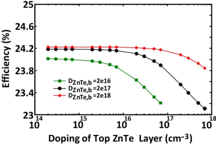
The variation of the doping concentration of the top ZnTe layer for different doping of bottom ZnTe layer are shown in figure. 5. Ass seen, the efficiency decreases when the doping
Figure 2: The configuration of the polycrystalline CdS/CdTe cell with step doping in the CdTe layer.
10
1410
1510
1610
1710
1820.5
21
21.5
22
22.5
23
23.5
Doping of Top CdTe Layer (cm-‐
3)
Ef
fici
en
cy
(%
)
DCdTe,b=2e18 DCdTe,b=2e16 DCdTe,b=2e17Figure 3: The efficiency of the designed cell as a function of doping concentration of top CdTe layer.
104
concentration of top ZnTe layer increases. Due to both high built-‐in electrical field and high absorption level, the efficiency was highest for doping concentration of 1015 cm-‐3. However built-‐
in electrical field and absorption are constant before doping concentration of 1015 cm-‐3. On other
hands, the built-‐in electrical field is low and the absorption is high after doping concentration of 1015 cm-‐3.
In order to achieve best device performance, various designs using different length of CdTe and ZnTe layers of diffraction grating were investigated. The charge storage time was decreased considerably to improve performance of the polycrystalline CdS/CdTe/ZnTe cell structure by increasing the length of CdTe of diffraction grating. Therefore, length of CdTe and ZnTe layers of diffraction grating were both optimized, however the doping concentration of the layers remained unchanged. The structure of polycrystalline CdS/CdTe/ZnTe cell with diffraction grating including CdTe and ZnTe layers was shown in figure. 6. Figure. 7 shows the cell efficiency of the new structure as a function of different length of CdTe and ZnTe layers of diffraction grating. As can be seen from figure. 7, the efficiency is maximum for 200 and 50 nm of CdTe and ZnTe layers in diffraction grating, respectively. As compared to the reference cell, polycrystalline CdS/CdTe/ZnTe cell with diffraction grating exhibited higher efficiencies. The best diffraction grating structure shows performance of 24.47% and a fill factor of 0.885, which is of particular importance in the solar cell design.
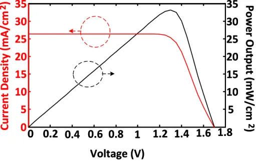
Figures. 8 and 9 show polycrystalline CdS/CdTe/ZnTe cell with tandem diffraction grating including CdTe and ZnTe layers and the current and power curves as a function of voltage, respectively. The results show the maximum conversion efficiency of 25.022% with the open circuit voltage, short circuit current density and fill factor of 1114 mV, 25.35 mA/cm2 and 0.8856, respectively under global AM 1.5 conditions.
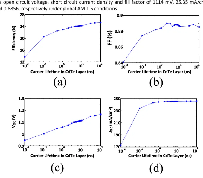
Since the carrier lifetime of CdTe has a strong influence on the solar cell fill-‐factor and the voltage calculation, we investigate the impact of carrier lifetime in the CdTe layer on the JSC, VOC,
FF and Efficiency of the proposed cell to improve the further efficiency. The variations of carrier lifetime can be modeled by variation of defect density. Increased defect density and purity of the CdTe alters the electron lifetime as well as the hole lifetime. Physically, a reduction in the defect density could be the key to improvement in increased lifetime through a smaller number of recombination centers. All carriers generated in the depletion region will be collected at higher lifetimes. Therefore, the VOC and conversion efficiency improve with increasing the carrier
lifetime. The VOC is defined as:
ln( 1) C C o O S J k V q J n T = + 1 where n is the ideally factor. k, T, q and JSC are Boltzmann's constant, absolute temperature,
electrical charge and short current density. J0 is dark current density that is directly linked to the
defect density and purity of the material. As can be seen, the VOC can be increased with
decreasing dark current density (Jensen, et al., 2016).
Figure. 10 shows the JSC, VOC, FF and Efficiency of cell as a function of carrier lifetime. As
seen, longer carrier lifetimes resulted in a higher VOC. Therefore, the conversion efficiency
increases with increasing carrier lifetime. data (Amin, et al., 2007).
10
1410
1510
1610
1710
1823
23.4
23.8
24.2
24.6
25
Doping of Top ZnTe Layer (cm-‐
3)
Ef
ficien
cy
(%
)
DZnTe,b =2e16 DZnTe,b=2e17 DZnTe,b =2e18Figure 5: The efficiency as a function of the top ZnTe layer doping concentration.
Figure 6: The schematic structure with diffraction grating including CdTe and ZnTe layers.
0.04 0.06 0.08 0.1 0.12 0.14 0.16 0.18 0.2 24.38 24.42 24.46 24.5 CdTe Length (µm) Ef fici en cy (% ) 0.05 µm 0.2 µm 0.1 µm 0.15 µm ZnTe Length (µm)
106 Figure 7: The cell efficiency as a function of different length of CdTe and ZnTe layers of diffraction grating.
Figure 8: polycrystalline CdS/CdTe/ZnTe cell with tandem diffraction grating including CdTe and ZnTe layers.
Voltage (V)
Cu
rr
en
t D
en
si
ty
(m
A/
cm
2)
0 0.2 0.4 0.6 0.8 1 1.2 1.4 1.6 1.8
0
5
10
15
20
25
30
35
5
10
15
20
25
30
35 Po
w
er
O
ut
pu
t (m
W
/c
m
2)
Voltage (V)
Cu
rr
en
t D
en
si
ty
(m
A/
cm
2)
0 0.2 0.4 0.6 0.8 1 1.2 1.4 1.6 1.8
0
5
10
15
20
25
30
35
5
10
15
20
25
30
35 Po
w
er
O
ut
pu
t (m
W
/c
m
2)
Figure 9: The power characteristics and current-‐voltage of the designed cell under global AM 1.5 conditions.
4. CONCLUSION
In this paper, a new structure is proposed which is achieved by diffraction grating and engineering absorber and back surface field layers in order to achieve the maximum efficiency. Also, the effect of carrier lifetime variation in the absorber layer on the conversion efficiency of solar cell was investigated. The results show the maximum conversion efficiency of 25.022% with
the open circuit voltage, short circuit current density and fill factor of 1114 mV, 25.35 mA/cm2
and 0.8856, respectively under global AM 1.5 conditions.
10-‐2 10-‐1 100 101 102 0.9 1 1.1 1.2 1.3
Carrier Lifetime in CdTe Layer (ns)
VOC (V ) 10-‐2 10-‐1 100 101 102 0.9 1 1.1 1.2 1.3
Carrier Lifetime in CdTe Layer (ns)
VOC (V ) 10-‐2 10-‐1 100 101 102 170 190 210 230 250
Carrier Lifetime in CdTe Layer (ns)
JSC (m A/ cm 2) 10-‐2 10-‐1 100 101 102 170 190 210 230 250
Carrier Lifetime in CdTe Layer (ns)
JSC (m A/ cm 2) 10-‐2 10-‐1 100 101 102 12 16 20 24 28
Carrier Lifetime in CdTe Layer (ns)
Ef fic ie nc y (% ) 10-‐2 10-‐1 100 101 102 12 16 20 24 28
Carrier Lifetime in CdTe Layer (ns)
Ef fic ie nc y (% ) 10-‐2 10-‐1 100 101 102 0.84 0.86 0.88 0.9
Carrier Lifetime in CdTe Layer (ns)
FF
(%
)
(a)
(b)
(c)
(d)
10-‐2 10-‐1 100 101 102 0.9 1 1.1 1.2 1.3Carrier Lifetime in CdTe Layer (ns)
VOC (V ) 10-‐2 10-‐1 100 101 102 170 190 210 230 250
Carrier Lifetime in CdTe Layer (ns)
JSC (m A/ cm 2) 10-‐2 10-‐1 100 101 102 12 16 20 24 28
Carrier Lifetime in CdTe Layer (ns)
Ef fic ie nc y (% ) 10-‐2 10-‐1 100 101 102 0.84 0.86 0.88 0.9
Carrier Lifetime in CdTe Layer (ns)
FF
(%
)
(a)
(b)
(c)
(d)
Figure 10: The variation of JSC, VOC, FF and Efficiency of the proposed cell as a function of the CdTe layer’s carrier
lifetime.
5. REFERENCES
Amin, N., Sopian, K., & Konagai, M. (2007). Numerical modeling of CdS/CdTe and CdS/CdTe/ZnTe solar cells as a function of CdTe thickness. Solar Energy Materials and Solar Cells, 91, 1202-‐1208.
Aramoto, T., Ohyama, H., & Kumazawa, S. (1997). 16.0% Efficient thin film CdS-‐CdTe solar. Jpn. J.
Appl. Phys., 36, 6304-‐6305.
Britt, J., & Ferekides, C. (1993). Thin-‐film CdS/CdTe solar cell with 15.8% efficiency. Applied
Physics Letters, 62, 2851-‐2852.
Colegrove, E., Banai, R., Blissett, C., Buurma, C., Ellsworth, J., Morley, M., & Sivananthan, S. (2012). High-‐Efficiency Polycrystalline CdS/CdTe Solar Cells on Buffered Commercial TCO-‐ Coated Glass. Journal of Electronic Materials, 41, 2833-‐2837.
108 Green, M. A., Emery, K., Hishikawa, Y., Warta, W., & Dunlop, E. D. (2016). Solar cell efficiency
tables (version 48). Progress in Photovoltaics: Research and Applications, 24, 905-‐913. http://www.silvaco.com/products/device_simulation/atlas.html.
Jensen, S. A., Burst, J. M., Duenow, J. N., Guthrey, H. L., Moseley, J., Moutinho, H. R., & Metzger, W. K. (2016). Long carrier lifetimes in large-‐grain polycrystalline CdTe without CdCl2.
Applied Physics Letters, 108, 263903.
Khosroabadi, S., Keshmiri, S. H., & Marjani, S. (2014). Design of a high efficiency CdS/CdTe solar cell with optimized step doping, film thickness, and carrier lifetime of the absorption layer. Journal of the European Optical Society: Rapid Publications, 9, 891-‐896.
Kosyachenko, L., Savchuk, A., & Grushko, E. (2009). Dependence of efficiency of thin-‐film CdS/CdTe solar cell on parameters of absorber layer and barrier structure. Thin Solid
Films, 517, 2386-‐2391.
Krishnakumar, V., Han, J., Klein, A., & Jaegermann, W. (2011). CdTe thin film solar cells with reduced CdS film thickness. Thin Solid Films, 519, 7138-‐7141.
Mahoodi, M., & Marjani, S. (2017). Performance enhancement of polycrystalline CdS/CdTe solar cell by diffraction grating and engineering layers. The 8th National Conference on Physics, 223-‐227.
Mahoodi, M., & Marjani, S. (2017). Enhanced photovoltaic performance of ultrathin polycrystalline CdS/CdTe solar cell via indium antimonide absorber layer. The 2nd
International Conference on Electrical Engineering (IC-‐EE)s, 1-‐4.
Mahoodi, M., & Marjani, S. (2017). High-‐efficiency polycrystalline CdS/CdTe/InSb/CdTe solar cell with step doping grading of absorber and back surface field layers. The 4th National
Conference on Information Technology, Computer and Telecommunication (ITCT), 1-‐7.
Mahoodi, M., Peiravi, A., & Marjani, S. (2018). Time to failure analysis of polycrystalline CdS/CdTe/InSb/CdTe solar cells. The 8th International Conference on Nanotechnology
(ICN), 1-‐3.
Marjani, S., Khosroabadi, S., & Sabaghi, M. (2016). A high efficiency ultrathin CdTe solar cell for nano-‐area applications. Optics and Photonics Journal, 6, 15-‐23.
Peña, J., Arés, O., Rejón, V., Rios-‐Flores, A., Camacho, J. M., Romeo, N., & Bosio, A. (2011). A detailed study of the series resistance effect on CdS/CdTe solar cells with Cu/Mo back contact. Thin Solid Films, 520, 680-‐683.
Razykov, T., Ferekides, C., Morel, D., Stefanakos, E., Ullal, H., & Upadhyaya, H. (2011). Solar photovoltaic electricity: Current status and future prospects. Solar Energy, 85, 1580-‐1608. Rios-‐Flores, A., Arés, O., Camacho, J. M., Rejon, V., & Peña, J. (2012). Procedure to obtain higher
than 14% efficient thin film CdS/CdTe solar cells activated with HCF2Cl gas. Solar Energy,
86, 780-‐785.
Sabaghi, M., Majdabadi, A., Khosroabadi, S., & Marjani, S. (2015). A novel ultrathin CdS/CdTe solar cell with conversion efficiency of 31.2% for nano-‐area application. The Progress in
Electromagnetics Research Symposium (PIERS), 1152-‐1155.
Sabaghi, M., Majdabadi, A., Marjani, S., & Khosroabadi, S. (2015). Optimization of high-‐efficiency CdS/CdTe thin film solar cell using step doping grading and thickness of the absorption layer. Orient. J. Chem.,, 31, 891-‐896.
Wu, X., Keane, J.C., Dhere, R.G., Dehart, C., Albin, D. S., Duda, A., Gessert, T. A., Asher, S., Levi, D. H., & Sheldon, P. (2001). 16.5% Efficient CdS/CdTe polycrystalline thin film solar cell. 17th
Conf. IEEE European Photovoltaic Solar Energy, 995-‐1000.