Abstract— The pristine boron nitride nanotubes have a large direct band gap around 5 eV. This band gap can be engineered by doping. We investigate electronic structure of the doped hexagonal boron nitride (5,5) nanotubes using the linearized augmented cylindrical wave method. In particular, this work focuses on systematical study of the band gap and the density of states around the Fermi-level when the nanotubes are doped by intrinsic impurities of two substitutional boron atoms in a super cell and a comparative analysis of the relative stability of three structures studied here. This corresponds to 3.3% of impurity concentration. We calculate 29 configurations of the nanotubes with different positions of the intrinsic impurities in the nanotube. The band gap and density of states around the Fermi level show strong dependence on the relative positions of the impurity atoms. The two defect sub bands called �� � appear in the band gap of the pristine nanotube. The doped nanotubes possess p-type semiconductor properties with the band gap of 1.3-1.9 eV.
Index Terms—Boron nitride nanotube, intrinsic impurity, band gap, density of states.
I. INTRODUCTION
In nanoscale simulations, one needs to consider the effects of a single atom on characteristics of
electronic and optoelectronic devices because the effects of the individual vacancies and impurities
start to have a real influence in the performance of the device.
There are two main steps in the nano electronic studies. The first one is a solution of the electronic
structure problem that deals with the electrons band energy of the material as well the density of states
at the energy levels. In practice, this study gives us the information about the band gap and the energy
levels where the electronic or optoelectronic device will work properly. For this purpose, different
theoretical methods are used in practice. Firstly, there are several ab initio approaches to solve the
Schrödinger equation which are based on the first principles. An example of such methods is the
linearized augmented cylindrical wave method (LACW) [1]. There exist also semi empirical methods
where the electronic structure is calculated by using adjustable parameters obtained for example from
experiments.
Analysis of Electronic Structure of Boron
Nitride Nanotubes with Different Positions of
Intrinsic Impurities
Fernando Gomes, Victor Dmitriev, Clerisson Nascimento
The second step in the nano device projects is the study of electronic transport, i.e., the behavior of
the electronic current inside the material. Here, the problem is usually to obtain the I-V
(current-voltage) characteristics. A combination of the Landauer approach with the non-equilibrium Green
function (NEGF) method is now widely used in the analysis and design of nanoscale devices.
Quantum transport in carbon nanotubes and other nano electronic devices is discussed in more details
in [2-7].
Advances in carbon nanomaterial science have stimulated interest in other kinds of nano materials,
in particular, in boron nitride nanotubes (BNNT), which were synthesized in laboratory in 1995 [8].
Structurally, BNNTs are III-IV compounds similar to carbon nanotubes [9,10]. BNNTs consist of a
tubular sheet with hexagonal bonding between boron and nitrogen atoms. The number of boron and
nitrogen atoms in the ideal nanotube is equal. It was shown that the ideal BNNTs possess the band
gap of about 5 eV which does not depend on the diameter of the nanotube, its chirality and the
number of the tube walls [11]. It is well known that depending on their geometry, carbon nanotubes
can be metallic or semiconductor [2]. Thus, in comparison with the carbon nanotubes the
independence of the BNNT band gap on geometry is a significant advantage from the point of view of
potential nano electronics and optoelectronics applications. However, the wide band gap restricts
severely the field of applications. Therefore, to find methods of tuning the band gap of BNNTs is very
important from the technological point of view. It was shown in [12], that the band gap of the BNNTs
can be narrowed by intrinsic defects (impurities) where some boron atoms are substituted by nitrogen
atom, and vice versa. Such defects are formed in the technological processes of the nanotube
synthesis [13]. Due to the presence of the intrinsic defects, a defect sub band � , � is formed and the band gap of the ideal BNNT is reduced.
In this work, we describe our results in study of BNNTs with intrinsic impurities with a view to
reduce the band gap of pristine BNNT. We analyze the influence of the relative position of the defects
on the electronic structure and density of state (DOS) using as the example the single wall armchair
type (5,5) BNNT. This tube has five-fold rotational symmetry and its diameter is = 6.6 . To solve the Schrödinger equation, we use the LACW method. In our analysis, the super cell formed by
three unit cells contains two defects of substitution of two nitrogen atoms by two boron atoms, which
corresponds to the impurity concentration of 3.3%. To see the influence of the position changes on the
band structure, we investigate systematically 29 possible nanotube configurations.
II. LINEARIZED AUGMENTED CYLINDRICAL WAVES METHOD
In this section, we describe shortly the LACW method. This is one of the most accurate methods in
the band theory of solids [1]. Generally, one of the main approaches in this theory is to write the
multi-electronic wave function � as a determinant formed from the wave functions of a single
� , , … , � = 1
√�! |
� � … ��
� … � … ��
� �
…
� �
…
… ��…�
| (1)
where 1/√ N! is the normalization factor, � represents the three spatial coordinates ( �, �, �) and � represents the single electron spin-orbital. Each spin-orbital is a product of �, �, � function that depends only on the spatial coordinates and the electron function . In the crystals or polymers that
have translational symmetry is called Bloch functions.
According to the approach above, the problem in the calculation of the energy bands of the
nanotube is reduced now to solve the Schrödinger equation for an electron:
�̂ =
,
(2)where n = 1, 2, .... . The Hamiltonian using the Rydberg normalization takes the form of Ĥ = − +
u r⃗ with the potential u r⃗ [8].
In order to simplify the calculations, Slater in 1937 proposed an approximation for the potential
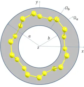
⃗ known as the muffin-tin (MT) potential approximation. This approach divides the crystal into two regions: �� which is the region around each atom in the crystal, where the potential is chosen to
be spherically symmetric depending only on the distance from the core enveloped by that sphere.
Within the sphere, the potential changes very rapidly. The second region �� is the region between
the spheres where the potential changes very slowly and therefore can be considered constant.
Movements of electrons in the nanotube are limited to a cylindrical shell with the thickness of
approximately twice the atomic van der Waals radius. Thus, it is assumed that the electronic motion in
the space between the MT spheres is limited by two cylindrical potential barriers that are impenetrable
to electrons, i.e., a barrier and with an outer and inner radius a and b, respectively. The radii
choice of a and b are made such that the volume between the barrier contains a substantial part of the
nanotube electron density. Fig. 1 shows some details of the model [1].
The calculation of the potential within the spheres of MT is based on the distribution of the total
nanotube electron density ⃗ . This distribution is taken as the superposition of the electron densities of each atom of the nanotube. The electrostatic potential �� ⃗ generated by the distribution ⃗ is obtained by the solution of Poisson's equation. Finally, the Coulomb potential � ⃗ is given by:
� ⃗ = �� ⃗ + � ⃗
,
(3)where � ⃗ is due to the positive charge of the atomic nucleus. The potential exchange interaction
�� ⃗ is a function of the distribution of the electron density ⃗ and is given by
�� ⃗ = −6� 83 ⃗ ⁄
, (4)
where α = 2/3. Equation (4) has been proposed by Slater and for many decades successfully used in
the calculation of band structures of crystals.
The solution of the Schrödinger equation for the region Ω consists of two solutions: one is for ��
and the other for �� region. The wave functions inside the cylindrical layer must be continuous and
smooth. A detail description of the method can be found in [1].
III. SIMULATION MODELS
In our numerical analysis, we consider the armchair (5,5) BNNT. Fig. 2a and 2b depicts the front
and side views of BNNT. The super cell chosen for calculations contains three unit cells. In Fig. 3,
the super cell represents the unrolled BNNT with 30 atoms of boron and 30 atoms of nitrogen shown
in red and yellow, respectively. The boron atoms are numbered from B1 to B30 and the nitrogen
atoms from N1 to N30.
N
B
(a) (b) (c)
Fig. 2. (a) Front view, (b) side view and (c) legend
TABLE I. NANOTUBE CONFIGURATIONS Configuration Positions of
boron atoms
Energy band gap , eV Energy gap � between the two �� � at point, eV
Config 1 N1 and N7
1.43, direct 1.08
Config 2 N1 and N25
Config 3 N1 and N13
1.78, indirect 0.22
Config 4 N1 and N19
Config 5 N1 and N4
1.42, indirect 1.43
Config 6 N1 and N28
Config 25 N1 and N6
Config 26 N1 and N30
Config 7 N1 and N10
1.84, indirect 0.31
Config 8 N1 and N22
Config 27 N1 and N12
Config 28 N1 and N24
Config 9 N1 and N16
1.90, indirect 0.12
Config 29 N1 and N18
Config 10 N1 and N2
1.70, indirect 0.94
Config 20 N1 and N3
Config 11 N1 and N8
1.81, indirect 0.08
Config 12 N1 and N26
Config 21 N1 and N9
Config 22 N1 and N27
Config 13 N1 and N14
1.92, indirect 0.07
Config 14 N1 and N20
Config 23 N1 and N15
Config 24 N1 and N21
Config 15 N1 and N5
1.33, direct 1.30
Config 16 N1 and N29
Config 17 N1 and N11
1.93, indirect 0.07
Config 18 N1 and N23
Config 19 N1 and N17
We place the first substitutional boron atom in an arbitrary point, for example, in point N1. In the
following, the position of this atom will serve as a reference for all other configurations. The position
of the second boron atom varies. Firstly, it can be put to the right or to the left from point N1 along
the circumference of the tube, i.e. in points N7, N13, N19, N25. Secondly, this boron atom can be put
at points N2 or N3, i.e. it can be moved along the axis of the tube. Thirdly, the second atom can be
displaced along the circumference and simultaneously, along the axis of the tube, for example, it can
be put in points N4, N10, N5, N11 etc. In Table I we give a description of the 29 simulated
configurations which comprise all the possible mutual positions of the two boron atoms in the super
cell.
IV. RESULTS AND DISCUSSION
At the beginning we shall make some general remarks concerning changes in the nanotube
the rotational symmetry of the (5.5) nanotube. As a result, the degeneracy of the bands is removed
and the DOS are broadened as was mentioned in [12]. Besides, some defects, such as for example,
config 5, remove the planes of symmetry which are perpendicular to the tube axis. In this case, one
can consider a chirality of the tube which appears due to the defects. A detail discussion of symmetry
induced properties of nanotubes can be found in [14].
We observe from the results of simulations that some of the settings lead to similar characteristics.
The configurations with the same electronic characteristics are grouped in Table I. For example,
configs 1 and 2 have the same electronic structure and DOS because these two configurations are in
fact the same nanotube (see Fig. 2). The same is true for configs 3 and 4, configs 5, 6, 25 and 26,
configs 7, 8, 27 and 28, configs 9, 13, 14, 23, 24 and 29, configs 10 and 20, configs 11, 12, 21 and 22,
configs 15 and 16 and configs 17, 18 and 19. All of the simulated structures correspond to p-type
semiconductors. The Fermi level is depicted in the figures below by the red line.
We analyze the simulation results from the point of view of the band gap ∆, the separation between the two defect sub bands � , given by ∆ and DOS. The results are summarized in Table I. We can see that the partial doping with intrinsic impurities significantly affects the band structure and
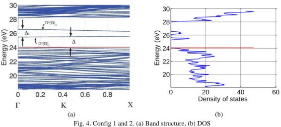
DOS of the BNNT with the appearance of two defect sub bands � . As an example, Fig. 4 shows
the energy band structure and DOS for config 1 and 2. The separation between the two defect bands at
point is 1.08 eV. The lowest of these two sub bands � can be considered as the bottom of the
conduction band which is unfilled. The valence band is completely filled. Thus one has in this case a
semiconductor of p-type with the direct band gap equal to 1.43 eV.
(a) (b)
Fig. 4. Config 1 and 2. (a) Band structure, (b) DOS
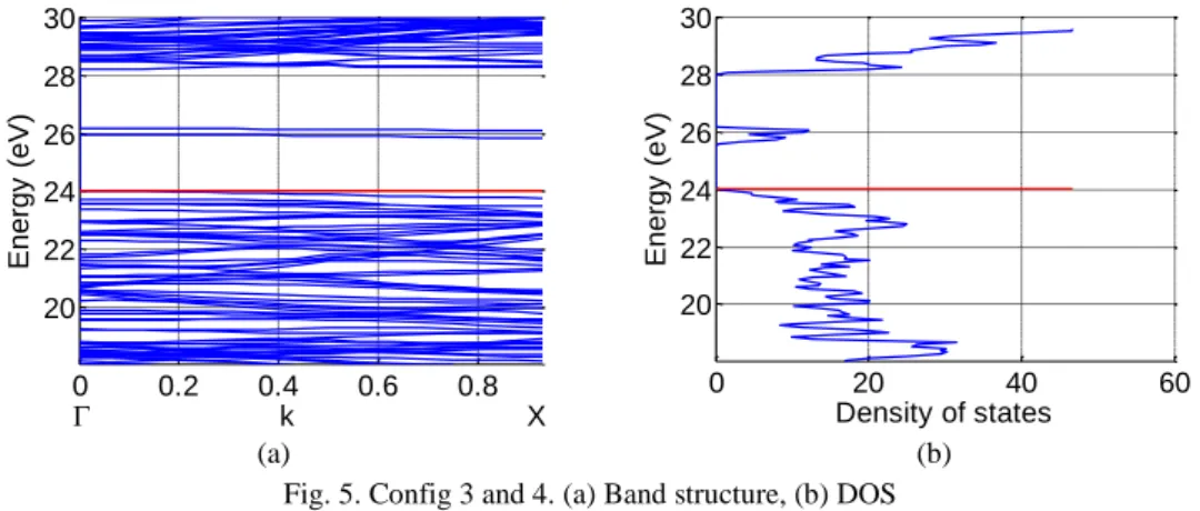
The results of simulations for config 3 and 4 are given in Fig. 5. These nanotubes have the indirect
band gap of 1.80 eV and the separation between the two defect sub bands � is now 0.22 eV at
point. Comparing Fig. 4 and Fig. 5, one can see that the increase of the radial distance between the
two doping atoms decrease the separation between the two corresponding defect sub bands �
and increase the separation between the Fermi level and the bottom conduction band.
0 20 40 60
20 22 24 26 28 30
Density of states
Ene
rgy
(a) (b) Fig. 5. Config 3 and 4. (a) Band structure, (b) DOS
Fig. 6 shows the band structure and DOS for configs 5, 6, 25 and 26. These configurations describe
a p-type semiconductor with the indirect band gap 1.42 eV and the separation between the two defect
sub bands � is now 1.43 eV at point. Fig. 7 shows the band structure and DOS for configs 7, 8,
27 and 28. These configurations possess the indirect band gap of 1.42 eV and the separation between
the two defect sub bands � is 0.31 eV at point.
(a) (b)
Fig. 6. Config 5, 6, 25 and 26. (a) Band structure, (b) DOS
(a) (b)
Fig. 7. Config 7, 8, 27 and 28. (a) Band structure, (b) DOS
Comparing Fig. 6 and 7, we observe that the energy band structure and DOS have a strong sensitivity
to the radial displacement of the intrinsic impurity atoms, but almost no sensitivity with respect to the
axial displacement of them along the BNNT. From simulations carried out, we noticed that when the
atoms of impurities are put close to each other, there is a strong interaction between them, and as a
0 0.2 0.4 0.6 0.8
20 22 24 26 28 30
k X
Ene
rgy
(eV)
0 20 40 60
20 22 24 26 28 30
Density of states
Ene
rgy
(eV)
0 0.2 0.4 0.6 0.8
18 20 22 24 26 28
k X
Ene
rgy
(eV)
0 20 40 60
18 20 22 24 26 28
Density of states
Ene
rgy
(eV)
0 0.2 0.4 0.6 0.8
18 20 22 24 26 28
k X
Ene
rgy
(eV)
0 20 40 60
18 20 22 24 26 28
Density of states
Ene
rgy
result, a smaller separation between the upper sub band of the top of the valence band and the lowest
of the bottom of the conduction band and a large separation between the two defect sub bands �
in comparison with those settings where the impurities atoms are put at a large distance from each
other. When the distance between these atoms along the circumference of the nano tube is increased,
this decreases the interaction between these two atoms and consequently, we observed the opposite
effect on the energy band structures of the BNNT under study, i.e., an increase and decrease occur in
the parameters and , respectively.
Finally, investigation the effect of separation between the impurity atoms in the axial direction of
the nano tube one should take into account the periodicity conditions imposed on super cell. The size
of the super cell under study is of three unit cells, and this is not large enough to simulate the real
doped process. So, there is a strong interaction between the substitutional dopant atoms and due to
this fact, increasing or decreasing the distance between the impurities atoms does not alter the energy
band structures and DOS of the BNNT, as we can see from Table I. This problem is discussed in
reference [15].
We have made also a quantitative analysis [16] about relative stability based on the total energy and
band gap value of three structures that we believe are quite representative of all configurations
studied. The structures analyzed are: a pristine BNNT, config 1 and config 4. The results are
summarized in Table II. According to Table II, one can see that pristine nano tube has the lowest total
energy and consequently, it is the most stable structure. Config 1 is less stable than pristine nano tube
and more stable than config 4. These results are in agreement with reference [11], which states that
the higher the band gap, the more stable this structure is.
TABLE II. CALCULATIONS RESULTS OF PRISTINE, CONFIG 1 AND CONFIG 2 NANOTUBE Pristine nano tube Config 1 Config 4
Total energy ( �) -10,612.74 -10,215.53 -10,215.48
Energy band gap ( � 4.1 1.78 1.43
V. CONCLUSION
We performed first-principles calculations of BNNTs using LACW method. 29 geometrical
configurations with different positions of two intrinsic boron atom impurities were systematically
studied. Our calculations show that for two substitutional boron atoms, the BNNTs demonstrate
p-type semiconductor characteristics. Two defect sub bands � appear inside the forbidden band.
The band gap width and the separation of the sub bands of the BNNT strongly depend on the relative
radial radial positions of the two atoms.
A quantitative analysis about relative stability based on the total energy and the band gap shows
that the pristine BNNT is the most stable structure in comparison with the doped nano tubes.
It is known that [12] that the intrinsic impurities due to nitrogen atoms produce the n-type
positions of these nitrogen atoms will also affect the band structure. This issue as well as an
investigation of the influence of the impurities with higher concentration will be the subjects of our
future work.
ACKNOWLEDGMENT
This work was financially supported by the Brazilian agencies CAPES and CNPq.
REFERENCES
[1] P. N. D`yachkov, "Augmented waves for nanomaterials," in Encyclopedia of Nanoscience and Nanotechnology, ed. by N. S. Nalwa, American Scientific Publishers, v. 1, pp. 191-212, 2004.
[2] H. S. Philip and D. Akinwande, Carbon nanotube and graphene device physics, Cambridge: Cambridge University Press, 2011.
[3] A. Javey and J. Kong, Carbon Nanotube Electronics, New York: Springer, 2009.
[4] K. Stokbro, D. E. Peterson, S. Smidstrup, A. Blom, M. Ipsen and K. Kaasbjerg, "Semiempirical model for nanoscale device simulations," Phys. Rev. B, vol. 82, 075420, 2010.
[5] A. Blom and K. Stokbro, "Towards Realistic Atomic-Scale Modeling of Nanoscale Devices," IEEE International Conference on Nanotechnology, pp. 1487-1492, August 2011.
[6] S. Datta, Quantum Transport: Atom to Transistor, Cambridge, UK: Cambridge Universty Press, 2005.
[7] Y. V. Nazarov and Y. M. Blanter, Quantum Transport. Introduction to Nanoscience, Cambridge: Cambridge University Press, 2009.
[8] N. G. Chopra, R. J. Luyken, K. Cherry, V. H. Crespi, M. L. Cohen, S. G. Louie, A. Zetti, “Boron Nitride Nanotubes,” Science, vol. 269, pp. 966-967, 1995.
[9] L. Xu, S. Li, Y. Zhang and Y. Zhai, “Synthesis, properties and applications of nanoscale nitrides, borides and carbides,”
Nanoscale, vol. 4, pp. 4900-4915, April 2012.
[10] J. Wang, C. H. Lee and Y. K. Yap, “Recent advancements in boron nitride nanotubes,” Nanoscale, vol. 2, pp.
2028-2034, June 2010.
[11] X. Blase, A. Rubio, S. G. Louie, M. L. Cohen, "Stability and Band Gap Constancy of Boron Nitride Nanotubes," Europhys. Lett., vol. 28, pp. 335-340, 1994.
[12] ] A. Y. Golovacheva and P. N. D`yachkov, "Effect of Intrinsic Defects on the Electronic Structure of BN Nanotubes," JETP Letters, vol. 82, pp. 737-741, 2005.
[13] P. Piquini, R. J. Baierle, T. M. Schmidt, and A. Fazzio, “Formation energy of native defects in BN nanotubes: ab initio study,” Nanotechnology, vol. 16, pp. 827-831, 2005.
[14] E. B. Barros, A. Jorib, G. G. Samsonidze, R. B. Capaz, A. G. S. Filho, J. M. Filho, G. Dresselhaus, M. S. Dresselhaus,
“Review on the symmetry-related properties of carbon nanotubes,” Phys. Rep., vol. 431, pp. 261-302, 2006.
[15] B. Huang, “Electronic Properties of Boron and Nitrogen Doped Graphene Nanoribbons and its Application for
Graphene Electronics,” Phys. Letters A, 375, pp. 845-848, 2011.