A High Speed Programmable Ring Oscillator
Using InGaZnO Thin-Film Transistors
Bhawna Tiwari
a, Shivam Kalla
a, Shashwat Kaushik
a, Ana Santa
b, Pydi Ganga Bahubalindruni
a,
V´ıtor Grade Tavares
c, Pedro Barquinha
b,
a IIIT-Delhi, Okhla Industrial Estate, Phase III, New Delhi, India - 110020
b i3N/CENIMAT, Department of Materials Science and Technology,
Universidade NOVA de Lisboa and CEMOP-UNINOVA, Campus de Caparica, 2829-516 Caparica, Portugal
c INESC TEC and Faculty of Engineering, University of Porto, Campus FEUP,
Rua Dr. Roberto Frias, 378, 4200-465 Porto, Portugal Abstract—This paper presents a high speed digitally
programmable Ring Oscillator (RO) using Indium-gallium-zinc oxide thin-film transistors (IGZO TFTs). Proposed circuit ensures high speed compared to the conventional ROs using negative skewed scheme, in which each inverter delay is reduced by pre-maturely switching on/off the tran-sistors. In addition, by controlling the load capacitance of each inverter through digital control bits, a programmable frequency of oscillation was attained. Proposed RO perfor-mance is compared with two conventional designs under same conditions. From simulation, it has been observed that the proposed circuit has shown a higher frequency of oscillations (283 KHz) compared to the conventional designs (76.52 KHz and 144.9 KHz) under same conditions. Due to the programmable feature, the circuit is able to generate 8 different linearly spaced frequencies ranging from 241.2 KHz to 283 KHz depending upon three digital control bits with almost rail-to-rail voltage swing. The circuit is a potential on-chip clock generator in many real-world flexible systems, such as, smart packaging, wearable devices, RFIDs and displays that need multi frequencies.
Keywords—Oxide TFTs, High speed programmable RO, negative skewed and rail-to-rail logic.
I. INTRODUCTION
Amorphous Oxide thin-film transistor (TFT) tech-nology is gaining significant interest due to its ability to provide transparent and flexible electronics at low cost with good stability [1] and improved performance compared to other competing TFT technologies like or-ganic and a-Si:H. Oxide TFTs find potential applications not only in display backplanes, but also in RFID tags [2], NFCs [3], data converters [4], smart packaging, biomedical [5]. However, lack of stable complementary type transistor (p-type) makes circuit design difficult, which is essential in building complete systems with this technology. Since CMOS design cannot be adapted directly, new circuit techniques have been developed to overcome this challenge [6][7][8].
Oscillators play a vital role as an on-chip clock generator in many circuits or systems, namely, data converters, DC-DC converters and wearable devices.
Ring Oscillator (RO) is a simple vehicle to obtain multi-phase clock signals. Applications like RFIDs, NFCs, and wearable systems (mainly ADCs) need clock signals with frequency at least in the order of hundreds of kilo-hertz. However, it should be noted that amorphous nature of the semiconductor in IGZO TFTs limits the mobility of the transistors and hence, the operating speed of circuits. Literature [9]-[14] reports ROs in oxide TFTs but, due to limited voltage swing, they are not suit-able as on-chip clock generator. Moreover, oscillators in [15],[16] are able to demonstrate full voltage swing but [15] has limited speed even though individual TFTs are showing a relative high mobility of 36 cm2/V.s and [16] employs dual-gate devices demanding more processing steps compared to single gate counterpart. In addition, all the designs are limited to generate a single frequency of oscillation. A voltage controlled oscillator (VCO) [17] demonstrates frequency of oscillations ranging from 400 Hz to 560 Hz, proportional to input control voltage. However, this frequency is quite low for afore-mentioned applications.
In order to address all the above challenges for a given technology, this work proposes a novel high speed RO that can ensure complete rail-to-rail operation with programmability (eight linearly spaced different frequencies). The proposed RO is able to demonstrate high frequency of oscillations using negative skewed delay scheme [18]. This technique reduces propagation delay of single stage inverter by prematurely triggering transistors. Since the output frequency of RO is inversely proportional to the propagation delay of single stage inverter, a considerable improvement in output frequency can be observed. The skewed scheme is effective in RO with CMOS inverters due to complementary behavior of transistors. Since oxide TFTs lack stable complementary (p-type) type transisors, it is challenging to adapt skewed scheme in conventional RO with diode-connected load inverter. Pseudo CMOS with bootstrapped load inverter mimics a CMOS inverter and ensures complete rail-to-rail operation. Therefore, pseudo CMOS with boot-strapped load inverter is slightly modified to design the
proposed RO using negative skewed delay scheme. In addition, the oscillator is made programmable such that the frequency of oscillations can be tuned to different frequency range. The programmability is achieved using control bits that set the load capacitance of each inverter, which directly controls the propagation delay and hence, oscillation frequency of RO.
The rest of the paper is organized as follows: Section II gives an overview about fabrication and modeling of IGZO TFTs; section III describes the proposed pro-grammable ring oscillator and the simulated results are presented in section IV. Finally, conclusions are drawn in section V.
II. DEVICEFABRICATION ANDMODELLING
Staggered bottom-gate IGZO TFTs, with top con-tacts, were fabricated on a glass substrate. Gate and source/drain electrodes of 60 nm thick Molybdenum (Mo) layer were sputtered and patterned by photolithog-raphy and dry etching. A 100 nm thick layer multi-component dielectric using SiO2 and T a2O5 was de-posited and patterned similar to gate and source/drain electrodes. Next, a 40 nm thick amorphous IGZO semi-conductor with a composition of In:Ga:Zn=2:1:1 (atomic ratio) [19] was sputtered to form the channel layer.
Towards the end, all devices were annealed at 180 ◦C
for 10 minutes in air. Once the devices were fabricated, the TFTs were characterized to obtain different device parameters. The mobility and oxide capacitance of the
device were reported to be around 13.8 cm2/V.s and
54 nF/cm2 from measurements, respectively. In-house
IGZO TFT model [20] was used to simulate circuits reported in this paper.
III. HIGH-SPEEDPROGRAMMABLERING
OSCILLATOR
A. High Speed RO
Negative skewed delay scheme, proposed in [18], is the simplest way to obtain high frequency of oscillations in RO by prematurely turning on/off one of the transis-tor in an inverter to speed up the transitions between ground and supply rails. Due to the absence of stable p-type transistors in oxide-TFTs, it is challenging to adapt the negative skewed delay scheme directly into the conventional RO with diode connected load based inverter. This is because providing negative delay to the input of driver transistors, to switch them on/off prematurely, will not reduce delay of an inverter stage as gate of load transistor is connected to power supply voltage. Therefore, transistors of diode connected load inverters in conventional RO, cannot be skewed using negative skewed delay scheme to obtain high frequency of oscillations. In order to take advantage of nega-tive skewed delay scheme, inverter which can mimic a CMOS counterpart is required. Pseudo-CMOS inverter using oxide TFTs reported in [21] can be an option,
however, in order to obtain complete rail-to-rail operation two different supply voltages are needed.
VOUT z z z z z z z z z (a) M3 M2 M1
v
OUT CBv
DD M4 z V IN z (b)Fig. 1. (a) Block diagram of 9 stage RO (b) Pseudo-CMOS inverter with Bootstrapped load.
Pseudo-CMOS inverter with Bootstrapped load [16] mimics a CMOS inverter and provides rail-to-rail op-eration without using additional power supply volt-age. Fig.1(a) shows the block diagram of 9 stage RO with Pseudo-CMOS bootstrapped load inverter, whose schematic is presented in Fig.1(b). In this inverter, boot-strapped capacitor, CB, is responsible for boosting output voltage to supply voltage, VDD, when logic 0 is applied to the input of inverter. On the other hand, when logic 1 is applied at the input, M 2 can be turned off completely through M 4 (typically WM 4≥ WM 3and the VDSM 4 is close to 0 V) which ensures rail-to-rail operation.
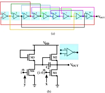
VOUT x x x x x x x y y y y y y y x x y y 1 2 3 4 5 6 7 8 9 (a) M3 M2 M1
v
OUT CB thv
DD M4 (i-6) x y ith x y (b)Fig. 2. (a) Proposed high speed 9 stage RO (b) Modified architecture of pseudo-CMOS inverter with bootstrapped load for proposed RO.
V
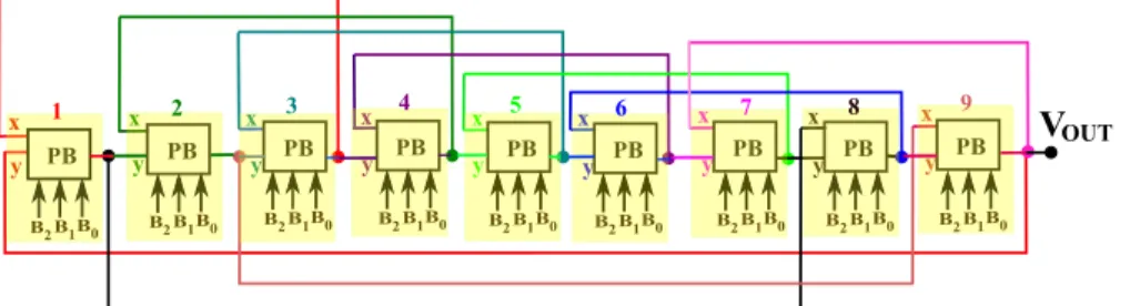
OUT x x x x x x x y PB y PB y PB y PB y PB y PB y PB x x y PB y PB B2B1B0 B2B1B0 B2B1B0 B2B1B0 B2B1B0 B2B1B0 B2B1B0 B2B1B0 B2B1B0 1 2 3 4 5 6 7 8 9Fig. 3. Proposed High Speed 9 stage programmable RO.
Fig.2(a) shows the block diagram of proposed high speed RO using negative skewed delay scheme. In this architecture, pseudo-CMOS inverter with bootstrapped load is modified slightly. As shown in Fig.2(b), gate of transistors M1 and M4 are separated as x and y, respectively, which are connected to the output of (i − 6)th stage and ith stage (for this particular case), respectively. This ensures premature triggering of M1 as x arrives earlier than y (Fig.2(b)), which in turn reduces the propagation delay of each inverter leading to high frequency of oscillations. In addition to high speed of operation, almost rail-to-rail swing can be ensured. B. Programmable High Frequency RO
The high speed RO discussed in the previous sub-section is made programmable in order to tune oscillator frequency over different frequency range. Frequency of oscillation, fclk, of n-stage RO, is given by:
fclk= 1 2.n.Tdelay
(1)
Here, Tdelay is propagation delay of an inverter in
RO. The propagation delay introduced by each stage is proportional to the load capacitance. Fig.3 shows the block diagram of proposed high speed programmable RO. Here, the inverters are replaced by programmable blocks (PB) which are controlled by bits B2(MSB), B1
and B0 (LSB).
Three binary weighted load capacitors controlled by three bits, B2, B1and B0, are connected at the output of inverter (of Fig.2(b)), as shown in Fig.4(a), to program the oscillator frequency. The load capacitance of an inverter is given by:
Cload = C(22B2+21B1+20B0) = 4CB2+2CB1+CB0 (2) From (2), it can be observed that whenever bits are set to logic high level, its corresponding capacitor is added to increase the load capacitance of an inverter. This increases the propagation delay and hence, reduces frequency of oscillation according to (1). C is the unit capacitor in (2),whose value should be selected carefully, especially when this approach is adopted for negative
B0 B1 B2 C 2C 4C x y (a) B0 B1 B2 4W x y 2W W x y PB B2B1B0 (b)
Fig. 4. Programmable block with (a) MIM capacitors (b) MOSCAPs.
skewed delay scheme. High value of C will cause excessive delay and make skewed operation difficult. Therefore, value of C is selected close to parasitic capacitors of the inverters in order to avoid any non-linearity in the operation of negative skewed delay RO. As a result, binary weighted capacitors can be realized using MOS capacitors (MOSCAPs), formed by n-type IGZO TFTs, whose widths are in the ratio 4:2:1 as shown in Fig.4(b) with same channel length. The schematic of Fig.4(b), hence, act as PB for proposed high speed programmable RO shown in Fig.3
IV. RESULTS ANDDISCUSSIONS
Circuit simulations have been carried out in Cadence Virtuoso using in-house IGZO TFT model at a supply voltage and device channel length of 10 V and 10 µm, respectively. First, in order to validate 9-stage high speed RO, conventional ROs with diode connected load inverter and pseudo CMOS bootstrapped load inverter have been designed and simulated on the same platform as that of 9-stage high-speed RO. The aspect ratios of the transistors used in different design for simulations are shown in
TABLE I. ASPECT RATIOS OFTRANSISTORS USED FOR SIMULATION OF DIFFERENTROS ROs Width (µm) Length (µm) With Diode-connected Load Inverter Driver 320 10 Load 40 10 With Pseudo-CMOS bootstrapped Load M2, M1 160 10 M3, M4 40 10 Proposed M2, M1 160 10 M3, M4 40 10
Table 1. In addition, the bootstrapped capacitor, CB, for pseudo bootstrapped load inverter, is kept as 5 pF.
0 10 20 30 40 50 60 70 80 0 5 10 0 10 20 30 40 50 60 70 80 0 5 10 Voltage (V) 0 10 20 30 40 50 60 70 80 0 5 10 Time (�s) Proposed diode−connected load inverter Pseudo CMOS bootstrapping load inverter
Fig. 5. Simulation Results of conventional and high-speed 9 stage ROs.
From the simulation results, shown in Fig.5, it can be observed that the high-speed RO, designed using negative delay skewed scheme, offers high frequency of oscillations compared to other conventional design. Table II summarizes performance metrics of high-speed RO and compares it with conventional ROs in terms of power, output swing and frequency of oscillations. It can be noticed that the proposed RO provides 95.3% im-provement in frequency of oscillations with 33.4% more power consumption compared to conventional RO with pseudo-CMOS bootstrapped load. As a result, power delay product is improved by proposed high speed RO (see Table II).
The high-speed RO is made programmable using external bits, B2, B1and B0and MOSCAPs with binary weighted widths as explained in the previous section. The widths of MOSCAP transistors are selected as 40 µm, 20 µm and 10 µm corresponding to bits B2, B1
and B0 for a channel length of 10 µm. Three
pro-grammable bits give 8 different frequencies of oscillation ranging from 241.2 KHz to 283 KHz as shown in Fig.6 with a step size of almost 6 KHz. From the figure, almost linear decrements in frequency of oscillation can be observed when the load capacitance at the output of the inverter is increased with increase in decimal equivalent values provided by programmable bits. For fine resolu-tion (step size), number of bits can be increased. Fig.7 shows the simulation results of programmable
high-speed RO under no load (B2B1B0 = 000) and full load (B2B1B0 = 111) conditions. 0 1 2 3 4 5 6 7 8 240 245 250 255 260 265 270 275 280 285 Decimal Equivalent of B2B1B0 Frequency (KHz)
Fig. 6. Staircase showing linearly spaced frequency of oscillations.
0 10 20 30 40 50 60 70 80 0 5 10 0 10 20 30 40 50 60 70 80 0 5 10 Time (�s) Voltage (V)
Output response of high−speed programmable RO for B2B1B0=111 Output response of high−speed
programmable RO for B2B1B0=000
Fig. 7. Simulation result of proposed 9 stage RO.
Table III compares the performance of the proposed oscillator with state of art work. It can be observed that for the first time programability is introduced in RO to obtain different frequency of oscillations. The RO reported in [9]-[14] have poor voltage swing, and therefore are not potential candidate for clock generators. It should be noted that the proposed RO gives better speed compared to RO reported in [15]. The RO in [15] is designed using transistors with a mobility of 36 cm2/V.s that is almost double the mobility of the transistors used in this work. On the other hand, dual gate transistors are used in [16] which requires additional processing step compared to single gate transistors. In comparison to the state of art work, the proposed circuit is able to provide high speed of operation and almost rail-to-rail output swing, with single gate transistors whose mobility is around 13.8 cm2/V.s. Speed can be further improved by employing self-aligned structures and devices with high electrical mobility.
V. CONCLUSION
This paper presents a high speed programmable RO with a-IGZO TFTs that can provide 95.3% improvement
TABLE II. PERFORMANCEMETRICS OFCONVENTIONAL ANDHIGH-SPEEDROS. 9-stage ROs Power Consumption (mW) Frequency of Oscillations (KHz) Output Voltage Swing (V) Power Delay Product (nJ) Conventional with Diode-Connected Load Inverter 0.930 76.52 6.05 0.675
with Pseudo CMOS
bootstrapped load inverter 2.069 144.90 10 0.793
Proposed 2.760 283.00 9.2 0.542
TABLE III. COMPARISON OFPROPOSEDROWITH STATE OF ART ∗Observed from reported results in state of art
ROs Stages Frequency (KHz) Voltage Swing∗ (% of supply voltage) Supply Voltage (V) Channel length (µm) Programability [9] 11 94.8 50 20 11 No [10] 11 47 60 15 9 No [11] 11 781 30 20 10 No [12] 11 810 48.6 25 9 No [13] 5 2100 0.5 25 10 No [14] 7 6510 3 20 6 No [15] 11 132 96 5 10 No [16] 13 360 100 20 6 No This Work 9 241.2-283 92 10 10 Yes
in frequency of oscillations compared to conventional RO at cost of 33.4% increment in the power consump-tion. In addition, for the first time programmability is introduced in the RO to achieve eight linearly spaced os-cillation frequencies ranging from 241.2 KHz to 283 KHz with a step size of around 6 KHz with 3 control bits. The proposed RO is able to provide a voltage swing of 92% of Vdd. Compared to state of art, this novel RO is able to deliver good performance parameters for a given technology. Hence it would find potential application as on-chip clock generator in smart packaging and wearable devices.
ACKNOWLEDGMENT
This work is supported by early career research grant with project ref. ECR/2017/000931.This work is funded by FEDER funds through the COMPETE 2020 Programme and National Funds through FCT - Por-tuguese Foundation for Science and Technology un-der the project number POCI-01-0145-FEDER-007688, Reference UID/CTM/50025. This work also received funding from the European Communitys H2020 program under grant agreement No. 716510 (ERC-2016-STG TREND) and No. 692373 (BET-EU).
REFERENCES
[1] T. Kamiya, K. Nomura and H. Hosono, ”Origins of High Mo-bility and Low Operation Voltage of Amorphous Oxide TFTs: Electronic Structure, Electron Transport, Defects and Doping,” in Journal of Display Technology, vol. 5, no. 7, pp. 273-288, July 2009.
[2] E. Cantatore T. C. T. Geuns G. H. Gelinck E. van Veenendaal A. F. A. Gruijthuijsen L. Schrijnemakers S. Drews D. M. de Leeuw ”A 13.56-mhz RFID system based on organic transponders” in IEEE J. Solid-State Circuits, vol. 42 no. 1 pp. 84-92 Jan. 2007.
[3] K. Myny and S. Steudel, ”16.6 Flexible thin-film NFC transpon-der chip exhibiting data rates compatible to ISO NFC standards using self-aligned metal-oxide TFTs,” 2016 IEEE International Solid-State Circuits Conference (ISSCC), San Francisco, CA, 2016, pp. 298-299.
[4] A. P. P. Correia P. M. C. Barquinha J. C. da Palma Goes A Second-Order ADC Using Sputtered IGZO TFTs New York NY USA:Springer 2015.
[5] E. Fortunato, N. Correia, P. Barquinha, L. Pereira, G. Goncalves and R. Martins, ”High-Performance Flexible Hybrid Field-Effect Transistors Based on Cellulose Fiber Paper,” in IEEE Electron Device Letters, vol. 29, no. 9, pp. 988-990, Sept. 2008. [6] Pydi Ganga Bahubalindruni, Bruno Silva, Vtor Grade Tavares,
Pedro Barquinha, Nuno Cardoso, Pedro Guedes de Oliveira, Rodrigo Martins, and Elvira Fortunato, ”Analog Circuits With High-Gain Topologies Using a-GIZO TFTs on Glass,” J. Display Technol. 11, 547-553 (2015).
[7] P. Bahubalindruni, V. G. Tavares, P. G. d. Oliveira, P. Barquinha, R. Martins and E. Fortunato, ”High-gain amplifier with n-type transistors,” 2013 IEEE International Conference of Electron Devices and Solid-state Circuits, Hong Kong, 2013, pp. 1-2. [8] P. G. Bahubalindruni et al., ”InGaZnO
Thin-Film-Transistor-Based Four-Quadrant High-Gain Analog Multiplier on Glass,” in IEEE Electron Device Letters, vol. 37, no. 4, pp. 419-421, April 2016.
[9] M. Mativenga, M. H. Choi, J. W. Choi and J. Jang, ”Transparent Flexible Circuits Based on Amorphous-IndiumGalliumZincOxide Thin-Film Transistors,” in IEEE Electron Device Letters, vol. 32, no. 2, pp. 170-172, Feb. 2011.
[10] M. Mativenga, D. Geng, J. H. Chang, T. J. Tredwell and J. Jang, ”Performance of 5-nm a-IGZO TFTs With Various Channel Lengths and an Etch Stopper Manufactured by Back UV Expo-sure,” in IEEE Electron Device Letters, vol. 33, no. 6, pp. 824-826, June 2012.
[11] X. Li, D. Geng, M. Mativenga and J. Jang, ”High-Speed Dual-Gate a-IGZO TFT-Based Circuits With Top-Dual-Gate Offset Struc-ture,” in IEEE Electron Device Letters, vol. 35, no. 4, pp. 461-463, April 2014. doi: 10.1109/LED.2014.2305665
[12] D. Geng, D. H. Kang and J. Jang, ”High-Performance Amor-phous IndiumGalliumZincOxide Thin-Film Transistor With a Self-Aligned Etch Stopper Patterned by Back-Side UV Exposure,”
in IEEE Electron Device Letters, vol. 32, no. 6, pp. 758-760, June 2011.
[13] A. Suresh, P. Wellenius, V. Baliga, H. Luo, L. M. Lunardi and J. F. Muth, ”Fast All-Transparent Integrated Circuits Based on Indium Gallium Zinc Oxide Thin-Film Transistors,” in IEEE Electron Device Letters, vol. 31, no. 4, pp. 317-319, April 2010. [14] Y. Chen, D. Geng, M. Mativenga, H. Nam and J. Jang, ”High-Speed Pseudo-CMOS Circuits Using Bulk Accumulation a-IGZO TFTs,” in IEEE Electron Device Letters, vol. 36, no. 2, pp. 153-155, Feb. 2015.
[15] J. D. Wu et al., ”A Low-Power Ring Oscillator Using Pull-Up Control Scheme Integrated by MetalOxide TFTs,” in IEEE Transactions on Electron Devices, vol. 64, no. 12, pp. 4946-4951, Dec. 2017.
[16] Y. Chen, D. Geng, T. Lin, M. Mativenga and J. Jang, ”Full-Swing Clock Generating Circuits on Plastic Using a-IGZO Dual-Gate TFTs With Pseudo-CMOS and Bootstrapping,” in IEEE Electron Device Letters, vol. 37, no. 7, pp. 882-885, July 2016. [17] T. Keragodu, B. Tiwari, Nishtha, P. Bahubalindruni, J. Goes
and P. Barquinha, ”A Voltage Controlled Oscillator Using IGZO Thin-Film Transistors,” 2018 IEEE International Symposium on Circuits and Systems (ISCAS), Italy, 2018 (Accepted)
[18] Seog-Jun Lee, Beomsup Kim and Kwyro Lee, ”A novel high-speed ring oscillator for multiphase clock generation using neg-ative skewed delay scheme,” in IEEE Journal of Solid-State Circuits, vol. 32, no. 2, pp. 289-291, Feb 1997.
[19] P. G. Bahubalindruni et al., ”Influence of Channel Length Scaling on InGaZnO TFTs Characteristics: Unity Current-Gain Cutoff Frequency, Intrinsic Voltage-Gain, and On-Resistance,” in Journal of Display Technology, vol. 12, no. 6, pp. 515-518, June 2016.
[20] Pydi Ganga Bahubalindruni, Vtor Grade Tavares, Pedro Bar-quinha, Cndido Duarte, Nuno Cardoso, Pedro Guedes de Oliveira, Rodrigo Martins, Elvira Fortunato, ”a-GIZO TFT neural model-ing, circuit simulation and validation, Solid-State Electronics,” Volume 105, 2015, Pages 30-36, ISSN 0038-1101.
[21] T. C. Huang et al., ”Pseudo-CMOS: A Design Style for Low-Cost and Robust Flexible Electronics,” in IEEE Transactions on Electron Devices, vol. 58, no. 1, pp. 141-150, Jan. 2011.