632 Brazilian Journal of Physics, vol. 34, no. 2B, June, 2004
Spin-Dependent Conductance in Nonmagnetic InGaAs
Asymmetric Double Barrier Devices
C. Moyses Araujo
1, A. Ferreira da Silva
1, C. Persson
2, R. Ahuja
2, and E. A. de Andrada e Silva
31
Instituto de F´ısica, Universidade Federal da Bahia, 40210-340 Salvador, Bahia, Brazil
2
Department of Physics, Uppsala University, P.O. Box 530, SE 751 21 Uppsala, Sweden
3
Instituto Nacional de Pesquisas Espaciais, CP515, S ˜ao Jose dos Campos, S˜ao Paulo, Brazil
Received on 31 March, 2003
The spin dependence of the conductance of an asymmetric double-barrier InGaAs device is studied within the multiband k·p and envelope function approximations. The spin-dependent transmission probability for electrons
across the structure is obtained using transfer matrices and the low bias conductance per unit area is calculated as a function of the Fermi energy (or doping) in the contacts. The possibility to obtain spin polarized currents in such devices is demonstrated, however, the resulting degree of polarization is rather small (a few percent) in the specific InGaAs structures considered here.
1
Introduction
The spin-orbit interaction allows the spin manipulation in nonmagnetic semiconductor devices. Besides the spin tran-sistor proposed by Data and Das [1], which is based on the Rashba spin-orbit term, of importance to the spintron-ics development, there have been, more recently, different proposals of nonmagnetic semiconductor spin filter devices [2, 3, 4]. However, in order to fabricate them, further inves-tigations are necessary in order to test these ideas in different structures and device geometries.
The physical effect behind these electron spin filtering devices is the resonant tunneling through spin-orbit split res-onances. The fabrication of the devices for such resonant tunneling experiments includes the creation of mesas in the multibarrier semiconductor structure and subsequent etch-ing, so that the back contact can be made in a doped epilayer near the substrate [4, 5]. In this case, the electric current will run as schematically illustrated in Fig. 1. As first suggested by Koga et al. [4], a spin-dependent electric current is ex-pected to be detected if the back contact is placed in only one of the sides, with opposite polarizations for right and left sided contacts.
A triple barrier structure with modulation doping was used in Ref. [4] to demonstrate the possibility of getting spin polarized currents in these resonant tunneling devices. In the present contribution, we consider instead structures with un-doped asymmetric InGaAs double barriers, and calculate the low bias conductance as a function of the Fermi energy (or doping) in the contacts. The results show that spin depen-dent electric currents are expected to run in such devices, but with a small polarization degree. Next, we describe the model calculation, present specific results for InGaAs/InP/ InGaAs/ GaAsSb/InGaAs asymmetric double barrier struc-tures and then summarize the main conclusions.
Figure 1. Schematic illustration of the resonant tunneling device structure and geometry, with an asymmetric double barrier and a sided back gate contact.
2
Spin-dependent conductance
C. Moyses Araujoet al. 633
Table I. Band and structure parameters used in the calculation.
Eg(eV) ∆(eV) m∗0(m0) Vc(meV) In0.53Ga0.47As 0.75 0.36 0.04 0
InP 1.42 0.11 0.08 180
GaAs0.5Sb0.5 0.81 0.75 0.04 360
At zero temperature, the corresponding low bias spin de-pendent conductance per unit area is given simply as [6]:
Gα= e2
m(EF)EF
4π2~2
Z π/2
0
dθsin(θ)cos(θ)Tα(EF, θ) ;
(1) whereEF is the Fermi energy at the doped InGaAs contact
layers,θcorresponds to the electron angle of incidence, (in the sum overkk),eis the electric charge,m(EF)is the
elec-tron effective mass (obtained from eight band Kane model) at the Fermi energy andTαis the spin dependent
transmis-sion probability (α = up or down, with respect to the di-rection perpendicular to both the growth and the sided back contact directions). The integral is done numerically and it is important to note that the integration overθ, between zero andπ/2, assures that we are counting only the electrons in the bottom contact that reach the gate positioned on the right side.
Finally, Tα(E, θ) is calculated following the transfer
matrix procedure described in reference [7]. It is based on Kane’s model for the bulk plus spin-dependent boundary conditions for the envelope functions [8].
3
Results
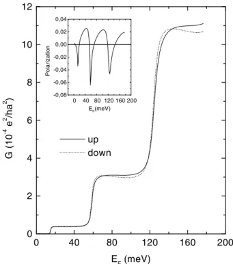
In Fig. 2, we show the obtained conductance, in units of
e2
/ha2
, where a stands for the effective Bohr radius, for both spin up and down electrons. We have considered 3 nm InP and GaAsSb barriers with a 20 nm InGaAs layer in be-tween (see Fig. 1). In Table 1, we list the band parameters used in the calculations, i.e. the band gapEg, the spin-orbit
splitting in valence band∆, the conduction band edge effec-tive mass and the conduction band offsetVc, of the different
lattice-matched III-V compounds.
One can see that the conductance in such devices, for both spin directions, shows typical steps as a function of the Fermi energy, corresponding to the quantized resonant states (the bottom of the subbands of quasi-bound states). With in-creasing Fermi energy, the steps in the conductance increase due to the increased transmission probability through the higher subbands. More interesting however, is the small dif-ference seen between the current for opposite spins, which increases withEF. This is the signature of the Rashba
ef-fect and the expected polarization efef-fect, similar to the one discussed in Ref. [4].
In the inset of Fig. 2, we show the obtained polarization calculated asP = (Gup−Gdown)/(Gup+Gdown). The
polarization is seen to be always rather small (only a few
percent) and to oscillate as a function ofEF, due to the
po-larization inversion at the incoming of each new subband.
Figure 2. Obtained spin-dependent conductance, per unit area, of the device in Fig. 1, as a function of the Fermi energy (or doping) in the contacts. The band parameters used in calculation are listed in Table 1. The inset shows the corresponding polarization, i.e.
P= (Gup−Gdown)/(Gup+Gdown).
4
Conclusion
Summarizing, we have studied the spin dependent conduc-tance through InGaAs double barrier structures with sided gated contacts. Our results demonstrate that it is possible to obtain spin polarized electric currents through such non-magnetic resonant tunneling devices. The predicted polar-ization, however, is of only a few percent. With a different, probably more sophisticated, device, we may be able to in-crease considerably such electric current spin polarizaztion. For example, it would be interesting to investigate similar effects in a resonant tunneling transistor, with an asymmet-ric superlattice [7] in the base, and high energy injection [9]. This work is in progress.
Acknowledgments
634 Brazilian Journal of Physics, vol. 34, no. 2B, June, 2004
References
[1] S. Datta and B. Das, Appl. Phys. Lett.56, 665 (1990). [2] E. A. de Andrada e Silva and G. C. La Rocca, Phys. Rev. B
59, R15583 (1999).
[3] A. Voskoboynikov, S. Shin Liu and C.P. Lee, Phys. Rev. B
59, 12514 (1999).
[4] T. Koga et al., Phys. Rev. Lett.88, 126601 (2002). [5] G. Reuscher et al.,Phys. Rev. B53, 16414 (1996).
[6] See, for example, J. H. Davies, The physics of low-dimensional semiconductors (Cambridge Univ. Press, Cam-bridge MA, 1998).
[7] C. Moyses Araujo, A. Ferreira da Silva and E. A. de Andrada e Silva, Phys. Rev. B65, 235305 (2002).
[8] E. A. de Andrada e Silva, G.C. La Rocca and F. Bassani, Phys. Rev. B55, 16293 (1997).