*e-mail: [email protected]
Characterization of Structural Alteration in Diamond Turned Silicon Crystal by
Means of Micro Raman Spectroscopy and Transmission Electron Microscopy
Renato Goulart Jasineviciusa*, Arthur José Vieira Portoa, Paulo Sérgio Pizanib, Jaime Gilberto Duducha, Francisco José Santosc
a
Laboratório de Engenharia de Precisão, Departamento de Engenharia Mecânica,
Escola de Engenharia de São Carlos, Universidade de São Paulo,
C.P. 359, 13566-590 São Carlos - SP, Brazil
b
Laboratório de Semicondutores, Departamento de Física, Universidade Federal de São Carlos,
C.P. 676, 13560-905 São Carlos - SP, Brazil
c
Departamento de Física, CCET, Universidade Federal de Mato Grosso do Sul,
C.P. 549, 790709-900 Campo Grande - MS, Brazil
Received: September 22, 2004; Revised: May 6, 2005
In this work, (100) oriented monocrystalline silicon samples were single point diamond turned under conditions that led to a ductile and brittle regime. Raman spectroscopy results showed that the ductile regime diamond turning of silicon surfaces induced amorphization and, on the contrary, in the brittle mode machining condition this amorphous layer does not exist. Ductile machined surface was found to be a mixture of crystalline and amorphous phases probed by (macro)-Raman spectroscopy. Transmission Electron Microscopy (TEM) analyses were then carried out in order to characterize the structural alteration in the machined surface and chips. The electron diffraction pattern of the machined surface detected a crystalline phase along with the amorphous silicon confirming the former results. The mechanism of material removal is widely discussed based upon the results presented here.
Keywords: semiconductors, single point diamond turning, phase transformation, ductile-to-brittle transition
1. Introduction
Monocrystalline semiconductors are normally considered to be fragile and exhibit brittle response under conventional machin-ing conditions. Furthermore, under particular critical conditions of depth and/or thickness of cut, it is possible to achieve the ductile mode material removal so as to generate a crack free surface. Plastic deformation during machining of crystalline brittle materials occurs by shear involving mechanisms of slip system activation and disloca-tion movement. Although it is well established that monocrystalline silicon exhibits limited dislocation mobility and, consequently, brittle behavior below 650 °C1, the anomalous plastic behavior of silicon
during machining experiments at room temperature has prompted new researches on this subject.
Results from high hydrostatic pressure2,3, microindentation4-8
and microscratching9,10 experiments have demonstrated that
dia-mond-cubic silicon transforms to the denser metallic β-tin structure at room temperature. Upon release of the pressure, a reversion to an amorphous semiconductor phase, with a cubic structure has been reported11. Based on these facts, new hypotheses were proposed in the
debate on the mechanism responsible for material removal in ductile regime diamond turning of semiconductor crystals. According to some reported results, it has been asserted that the ductile behavior has its results, it has been asserted that the ductile behavior has its origin attributed to this phase transformation induced by pressure/ stress12. Cross-section studies carried out on a surface after diamond
turning of silicon13,14 indicates an amorphous phase in the outer most
surface, providing support to this hypothesis of phase transformation. However, nothing was mentioned about the presence of crystalline phase immersed in an amorphous medium in silicon. This fact can be important for the optical fabrication of semiconductor crystals by
means of mechanical grinding since this amorphous surface phase has to be considered as a barrier layer with a different refractive index from that of the substrate15.
Raman scattering can be considered a powerful characterization technique to evidence structural alteration in semicondutors materials because the vibrational spectrum of the material is greatly influenced by disorder and residual strains. These lead to changes in phonon frequencies, broadening of Raman peaks and breakdown of Raman selection rules16. For bulk crystalline Si (c-Si), the triple degenerated
optical phonons display in the first-order Raman spectrum one sharp peak at 521 cm-1. Due to the positive phonon deformation potentials
of Si, compressive (tensile) strains lead to a positive (or negative) frequency shift. On the other hand, due to the loss of phonon cor-relation length and the consequent breakdown of the q = 0 Raman selection rules (q is the phonon wave vector), disorder effects can lead to an asymmetric broadening and shifting of Raman peaks compatible with the dispersion relation of the material17. In the silicon case, the
frequency and asymmetry point to lower values because the disper-sion relationship presents decreasing optical frequencies, increasing phonon wave vectors. At maximum disorder (amorphous material, a-Si), the first-order Raman spectrum reflects the phonon density of states: it presents two broad bands centered at about 100 cm-1 (acoustic
band) and 470 cm-1 (optical band)18.
Recently, new information has been added to discussion on the multiple phase found in silicon after mechanical deformation by microindentation with spherical indenter19-23. The microstructure
micro-scopy, consisted of specific phases of silicon which were formed in the second and subsequent indentation cycles under low loads19,20.
An increase of the maximum load causes changes in subsequent indentation cycles making phase transformation events to occur ear-lier on both loading and unloading21. It was also reported that when
the maximum load increases a crystalline phase of high pressure of body centered-cubic (named Si-III) and rhombohedral (Si-XII) can appear22. Furthermore, different amorphous structures have been
induced in monocrystalline silicon by high pressure in indentation and polishing23. Transmission electron microscopy and
nanodiffrac-tion study of the indentananodiffrac-tions and polished samples showed that the structures of silicon formed at slow and fast loading/unloading rates are dissimilar and inherit the nearest-neighbor distance of the crystal which are formed (idem). These results are concerned with spherical indenters. Ge and collaborators have also made interesting finding in this area using nanoindentation with Berkovich indenter24,25. The
authors proposed that a mechanism of dislocation-induced lattice rotation that leads to phase transition and distortion-induced amor-phization during nanoindentation. Furthermore they used Raman spectroscopy and transmission electron microscopy to investigate the temperature effects on the stability of metastable silicon phases (Si-III and Si-XII) produced by nanoindentation. It was found that the thickness of the specimen beneath the residual imprint plays an important role in the phase transformation sequence during heating up to 200 °C25.
Gogotsi et al. (2001) probing wear debris generated by scratching silicon with indenters of different geometries also detected polic-rystalinity. Besides amorphous silicon, they found Si-III, Si-XII and Si-IV26. This is an important finding since during scratching there is
a dynamic component which is similar to machining process. More recently, Zarudi et al.27 have shown that the size of the amorphous
transformation zone and the depth of slip penetration in sample subsurface were mainly dependent on the stress field applied in scratching monocrystalline silicon. They reported an investigation on the effect of temperature and stress on plastic deformation in scratching using dry air, coolant, and liquid nitrogen. The influence of the temperature variation of - 196 °C was surprisingly small and the low temperature did not suppress the phase transformation and dislocation activity27.
Despite of all efforts to investigate the effects of diamond turning upon the machined surface, there are still some aspects to be inves-tigated. The machined surface is not totally amorphous as reported before. Amorphous phase along with remnant crystalline phase should be expected based upon evidences with other semiconductors. The mechanism involved with material removal may not rely only upon total phase transformation of the material removed. These aspects will be discussed in this paper.
In this work, an original (macro)-Raman investigation of single point diamond turned monocrystalline silicon (100) oriented samples machined in ductile and brittle modes is presented. All measurements were performed at room temeperature, with special care taken to avoid overheating the samples. Transmission Electron Microscopy (TEM) planar and cross-section view analyses were also carried out after machining in order to characterize the structural alteration in the machined surface and chips.
2. Experimental Details
Ductile regime diamond turning tests were carried out on a commercially available diamond turning machine. Facing cuts were performed on monocrystalline silicon polished samples (10 x 10 mm2)
and 500 µm thick with (100) surface orientation. The cutting condi-tions were 2.5 and 8.0 µm/rev feed rate and 5 µm nominal depth of cut. The crossfeed direction was from outside to inside. These
conditions provided ductile and brittle modes during machining, with mirror-like and opaque surface finish. A scanning electron mi-croscope Zeiss, model DSM 960, operated with an electron beam of 20 kV was used for the observations of the chips. Figure 1 gives the schematic diagram illustrating the machining geometry with round nose tool. Only fresh diamond tools were used to perform the cutting tests. The single point tools used in this work were round nose single crystal diamond tools (Contour Fine Tooling). Table 1 describes the experimental conditions and tool geometry used in the cutting test. Synthetic water soluble oil was used as lubricant and coolant during turning. Atomic force microscopy (AFM) was used in order to probe the surface machined in the ductile regime. It was operated with a standard 50-60° conical silicon nitride stylus of 15-20 nm radius tip, with cantilever spring constant of ~ 0.06 N/m. Conventional contact mode was employed where the stylus is scanned raster style over, with contact forces of typically 10-100 nN.
The Raman measurements were performed using a U1000 Jobin-Yvon spectrometer. To probe the depth profile of disorder ef-fects, the 457.9, 488.0 and 514.5 nm lines of an argon ion laser were used. For these lines, the penetration depth is about 140, 270 and 340 nm for c-Si, respectively. The laser power was kept low at about 200 mW, in order to avoid heating effects and a cylindrical lens was used. For amorphous silicon (a-Si), the optical absorption coeficient can reach one order of magnitude higher, leading to penetration depths of about tenths of nanometers, depending on the degree of amorphiza-tion28,29. The machined sample was annealed in a LINKAN TS 1500
micro furnace attached to a Micro Raman spectrometer. attached to a Micro Raman spectrometer.
A Transmission Electron Microscope, operated at 200 kV was used to conduct the observation of chips and surface. The chips observed were those left on the machined surface after the cutting tests. The silicon chips were suspended in isopropyl alcohol, and the mixture was then deposited onto a copper TEM grid (Formvar support or lacey carbon film). The silicon machined sample was cut into 2 mm2 squares
Table 1. Tool geometry and cutting conditions used in the cutting tests.
Tool Geometry Dimensions
Tool nose radius (mm) 0.65
Rake angle (°) - 25
Clearance angle (°) 12
Spindle speed (rpm) 1000
Feed rate (µm/min) 2.5 and 8.0
Depth of cut (µm) 5
Diamond Tool
Workpiece
Machined Surface R
p+
dc
f Cutting direction
f - feed rate dc - depth of cut Rp - tool nose radius tmax - maximum chip thickness
tmax Feed direction
Vol. 8, No 3, 2005 Means of Micro Raman Spectroscopy and Transmission Electron Microscopy 263
and lapped and polished (with 5 µm and 1 and 1 µm SiC abrasive) from the unmachined surface to a thickness of < 50 µm. The sample was then affixed to a copper-slotted TEM grid using epoxy and dimpled via argon ion milling to provide an electron-transparent central area.
3. Results
Three-dimensional AFM images of the surfaces diamond turned in the ductile and brittle modes are shown in Figure 2. In Figure 2a, the cross-feed of the cutting tool is 2.5 µm rev-1. The cut grooves can
be clearly seen, regularly spaced and running parallel with cutting direction which confirms the absence of chatter vibration. The surface roughness is 1.6 nm Ra. In this case single point diamond turning has achieved fully ductile material removal. A closer examination of the machined surface in Figure 2b (f = 8.0 µm/rev) indicates that micro-cracks are present and brittle mode prevailed. The surface roughness measured is 91.25 nm Ra. Figure 3 presents a SEM photomicrograph of typical silicon chips removed in the ductile mode.
Figure 4a shows the characteristic Raman peak of crystalline Si at 521.6 cm-1 from the sample before the cutting tests, and Figures 4b
Mm
x z
10,000Mm 500,000 nm 10
20
30
40
40 30 20 10
Mm
si81.001 x z
10,000Mm 1000,000 nm
Figure 2. Typical three-dimensional surface finish of the single-point diamond turned specimen obtained by atomic force microscope. The surface finish is smooth and damage-free. a) The cut grooves can be clearly seen, regularly spaced and running parallel with cutting direction which confirms the ab-sence of chatter vibration; b) Examination of the machined surface under brittle regime shows that microcracks are present. The cutting conditions
f = 2.5/8.0 µm rev-1 (respectively) and d
c = 5 µm, and the tool has 0.65 mm
nose radius and - 25° rake angle. (b) (a)
Figure 3. Scanning electron micrography of a chip left on the surface of the machined silicon sample in the ductile regime. The ribbon-like chips indicate a plastic flow characteristic of ductile mode.
440 480 520
0 a) b) c)
X 60
Raman Shift (cm-1)
Intensity (a.u.)
and 4c show the Raman spectrum of the machined sample in the ductile and brittle modes, respectively. In both cases 488.0 nm exciting light was used. Compared with Figure 4c, Figure 4b shows the severe intesity reduction of the crystalline silicon (c- Si) Raman peak at 521.6 cm-1 (linewidth of 4.8 cm-1) by a factor of about 60 and
the presence of a new broad band centered at about 470 cm-1 can
be noticed, which can be atributed to the optical band of a-Si. It is interesting to observe that, except for the reduction of the intesity by a factor of about five (Figure 4c), the frequencies and linewidths (4.3 an 4.6 cm-1, respectively) are within the experimental resolution,
indicating that the machining in brittle mode does not cause short range structural disorder or residual strains in the Si lattice. Moreover, the lack of any feature at about 470 cm-1 is indicative of the absence
of an amorphous phase.
The spectrum shown in Figure 4b could result from a thin amorphous layer at the machined surface of the sample, with thick-ness smaller than the penetration depth of the light, or a thick layer composed of microcrystallites immersed in an amorphous media, with a thickness greater than the penetration depth of the light. In the latter or former case, it is expected that the intensity ratio of the amorphous-to-crystalline Raman peaks be independent of (or dependent) on the penetration depth of the light. To probe these two possibilities, Raman measurements were performed using three different wavelengths of exciting light, having different penetration depths, as described previously. Comparing the results shown in Figures 5a-5c it can be seen that the intensity ratios (amorphous and crystalline) are about the same, thus indicating the region sampled by the light is composed of microcrystallites within an amorphous medium. However, the spectra do not show any signs of metastable phases such as those found in the literature19-26.
In order to characterize the structure of both surface and chips after machining, TEM analyses were carried out. Figure 6 shows a bright-field TEM image of a small part of a ribbon-like chip. The left portion of the chip displays the electron diffraction pattern from the chip which shows clearly a diffuse halo ring (Figure 6b) mean-while the right region displays both halo rings and diffraction spots (Figure 6c). The electron diffraction pattern on the left means that this
part of the chip is amorphous and the electron diffraction on the right is indicating that remnant crystalline phase is still present immersed in an amorphous medium.
Figure 7 shows a TEM image of the surface and the diffraction pattern. Figure 7a displays a bright field TEM micrograph showing a general view of the machined surface with the equally spaced cut-ting grooves generated on silicon (100). No signs of dislocation and microcracks are seen to be developed within the cutting grooves. The electron diffraction pattern from this the selected area (in Figure 7a) shows both halo rings and diffraction spots is shown in Figure 7b. This area can be considered the thinner edge of the electron-transparent central area. However, in the diffraction pattern it can be seen that halo rings are superposed on the diffraction spots of the crystalline Si.
Figure 8 shows a cross sectional TEM image of the turned sample perpendicular to the cutting direction and the correspondent diffraction pattern. This bright field cross section TEM micrograph shows dislocations and microcracks as can be seen underneath the dark gray outmost layer which was identified as the amorphous
440
Raman Shift (cm-1)
Intensity (a.u.)
480 520
c)
b)
a)
Figure 5. Raman spectra of silicon sample machined in ductile regime for exciting lines: a) 488.0 nm; b) 457.9 nm; and c) 514.5 nm wavelengths.
Figure 6. a) Bright-field TEM image of a part of a ductile chip; b) electron diffraction pattern which indicates that the structure of chip is amorphous; c) electron diffraction pattern which indicates that the structure of chip is amorphous and crystalline.
Figure 7. a) Plan-view TEM micrograph of a diamond turned region on the (001) Si surface and; b) electron diffraction pattern from the selected area (corresponding to the thinner edge of the electron-transparent central area).
(a)
(b) (c)
(a)
Vol. 8, No 3, 2005 Means of Micro Raman Spectroscopy and Transmission Electron Microscopy 265
layer formed after machining. This assert is based on the diffraction pattern from this area which contains both halo rings and diffraction spots as shown in the detail in Figure 8. The diffraction spots of the crystalline Si is from the portion of material underneath and within the amorphous layer. The amorphous layer is estimated to be in the range of 50 nm.
Figures 9a-9d show Raman spectra obtained during annealing of the machined sample with in situ analysis in a microfurnace, under annealing temperature of 200 °C, 400 °C and 600 °C, respectively. It is worth mentioning that in Figure 9a both amorphous and crystalline
phase are present. The spectra depict an expected shift of the Raman peak to lower frequencies due to the softening caused by the increase in temperature. Meanwhile, the amorphous phase clearly decreases with temperature. The absence of any feature about 470 cm-1 in
Fig-ure 9d is indicative of the crystalline recovery. After annealing, the crystalline phase is recovered and is characterized by the repositioning of the silicon peak (521.6 cm-1) (Figure 10).
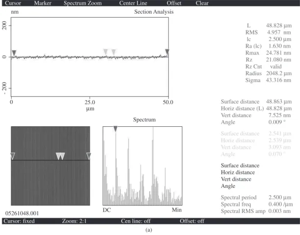
Figure 11 shows a comparative section analysis of the surface machined and annealed by heat treatment. The surface finish is slightly different in the heat-treated surface, i.e., the peak-to-valley surface roughness increased with the heat treatment. This can be better evaluated by means of the Rmax parameter which estimate the peak-to-valley height. The value of Rmax was increased from 24.78 nm (after machining) to 39.88 nm in the heat-treated sample. The same trend was noticed in the Ra value. The value of Ra increased from 1.6 nm to 2.2 nm after annealing. This increase in the height parameter does not find any explanation in the literature.
4. Discussion
The ductile regime was achieved under the cutting conditions applied in the cutting tests. This was clearly shown by the regular-ity of the cutting grooves and formation of ribbon-like chips. The mechanism responsible for chip formation process, in the ductile mode, might be the same for metals. A lamellar structure is formed in the free surface of the chip resembling those formed when ductile metals are machined. This anomalous plasticity is recognized to be resultant from the intermediate pressure/stress metallic phase transformed material.
The Raman scattering results demonstrated that ductile diamond turned silicon surfaces lead to amorphization. On the contrary, brittle regime machining does not generate amorphization within the surface. The Raman spectrum of the outmost layer of the sample machined in the ductile mode was found to be a mixture of crystalline and amorphous phases. Comparing the Raman spectra from brittle mode conditions, it is clear that tool-workpiece interaction is insufficient to produce amorphization. It is important that the machining parameters remain within certain conditions: the machining condition must lead to the phase trasnformation and consequently to the ductile mode of machining.
Figure 8. TEM cross sectional image of the machined sample and the dif-fraction pattern respectively.
Annealing Temperature
Intensity (counts/s)
a) 20 °C b) 200 °C c) 400 °C d) 600 °C 1.75
1.50
1.25
1.00
0.75
Raman Shift (cm-1)
250 300 350 400 450 500 550
a-Si Si
/10
d
c
b
a
Figure 9. Raman spectra of the silicon (100): a) monocrystalline silicon after machining at room temperature of 20 °C; b) machined surface during annealing (200 °C); c) machined surface during annealing (400 °C); and d) machined surface during annealing (600 °C).
440 460 480 500 520 540 560 580
1.4 1.6 1.8 2.0
2.2 b)
a)
/ 50
Intensity (counts/s)
Raman Shift (cm-1) a) 600 °C
b) 20 °C (after annealing)
Figure 11. Images made by AFM of section analysis of the ductile diamond turned silicon surfaces: a) machined surface without heat treatment; and b) ma-chined surface after annealing.
(a)
(b)
L RMS
lc Ra (lc) Rmax Rz Rz Cnt Radius Sigma
48.828Mm 4.957 nm 2.500Mm 1.630 nm 24.781 nm 21.080 nm
valid 2048.2Mm 43.316 nm
Surface distance Horiz distance Vert distance Angle
48.863Mm Surface distance
48.828Mm Horiz distance (L)
Vert distance 7.525 nm Angle 0.009 °
Surface distance 2.541Mm
Horiz distance 2.539Mm
Vert distance 3.093 nm
Angle 0.070 °
Spectral period 2.500Mm Spectral freq 0.400 /Mm Spectral RMS amp 0.003 nm Section Analysis
nm
Mm
50.0 25.0
- 200
0
0
200
Spectrum
DC Min
05261048.001
Cursor Marker Spectrum Zoom Center Line Offset Clear
Cursor: fixed Zoom: 2:1 Cen line: off Offset: off
L RMS
lc Ra (lc) Rmax Rz Rz Cnt Radius Sigma
49.902Mm 7.544 nm 2.497Mm 2.217 nm 39.883 nm 34.604 nm
valid 4694.0Mm 18.384 nm
Surface distance Horiz distance Vert distance Angle
50.018Mm Surface distance
49.902Mm Horiz distance (L)
Vert distance 8.745 nm Angle 0.010 °
Surface distance 2.544Mm
Horiz distance 2.539Mm
Vert distance 7.738 nm
Angle 0.175 °
Spectral period 2.497Mm Spectral freq 0.400 /Mm Spectral RMS amp 0.002 nm Section Analysis
nm
Mm
50.0 25.0
- 200
0
0
200
Spectrum
DC Min
05261108.001
Cursor Marker Spectrum Zoom Center Line Offset Clear
Vol. 8, No 3, 2005 Means of Micro Raman Spectroscopy and Transmission Electron Microscopy 267
TEM analyses of the chips have not shown any signs of disloca-tion activity and sharp striadisloca-tions parallel to the machining direcdisloca-tion. This can be attributed to the interaction between the cutting edge imperfections with material. However, crystalline and amorphous phase were detected in opposite positions of the same chip. The amorphous character of the chip was probed by electron diffraction pattern showing only diffuse halo rings is likely to be formed closely to the tool center where the pressure and stress are more intensive during machining (Figure 1). The different electron diffraction pat-tern with halo rings and diffraction spots present in the chip may be attributed to the fact that the chip may undergo a decompression along the width of cut (Figure 1) so as the pressure is not high enough to induce full phase transformation in this portion of the chip. The diffraction pattern of the machined surface indicates that remnant crystalline silicon is embedded in an amorphous Si phase. This result corroborates well with that of Suzuki and Ohmura1 which
demon-strated that this detected amorphization has to be considered on a diffraction scale and possibly it can be considered to be a polycrystal formed by nanocrystals.
The heat treatment proceeded showed that the surface crystallin-ity was recovered but the microtopography of the machined surface undergone an expansion. This is might be an expected result since that contrary was the most unlikely to occur. It is known that when the intermediate β-Sn (Si-II) structure forms from the diamond structure (Si-I) there is volume decrease of 22% (denser phase) and when the pressure is released the amorphous phase is still with 8% decrease in volume. Consequently, it would be expected that after the annealing there would be a volume recovery and a surface roughness increase. It is worth mentioning that the crystal phase recovery with annealing heat treatment is important to the fabrication of high quality compo-nents as it was shown in this paper.
5. Conclusions
This paper showed that silicon can be machined in the ductile mode at room temperature when appropriate cutting conditions are used. Ribbon-like chips are formed during cutting in the same way as is observed when ductile metals are cut. On the contrary when the cutting conditions are above the critical conditions, the brittle failure is the predominant mode.
Raman spectra results called the attention to the presence of a crystalline phase in an amorphous medium. However, the crystalline peak (at 521 cm-1), could be attributed to the fact that 488.0 nm lines
of an argon laser, used as an exciting light, can probe the depth profile of disorder effects up to 270 nm for crystalline silicon and some tenths of nanometers in amorphous silicon. Based on this assumption it is possible that Raman scattering is probing also a crystalline phase from underneath the surface vicinity.
TEM planar and cross sectional views were also conducted and diffraction pattern indicated that remnant crystalline silicon is embedded in amorphous Si phase in the planar view. Structural and morphological TEM analyses of both chip and surface produced in ductile regime diamond turning were also carried out. No sign of dislocations was detected in the electron diffraction pattern of some portion of the chip. The chip is partially amorphous and since the electron diffraction is carried out in the opposite side of the chip, a mixture of crystalline and amorphous phase is detected. This dif-ference is attributed to a pressure decrease along the width of cut during machining.
The heat treatment carried out showed that it is possible to recover the crystalline phase of the transformed surface layer.
The use of two different characterization techniques, Raman spectroscopy along with microscopy, demonstrated a powerful tool
to investigate surface and subsurface integrity of diamond turned semiconductors single crystals.
Acknowledgments
The authors would like to acknowledge the finnacial support by FAPESP, CNPq and CAPES (Brazil).
References
1. Suzuki T, Ohmura, T. Ultramicroindentation of silicon at elevated
tem-peratures. Philosophical Magazine A. 1996; 74(5):1073-1084.
2. Minomura S, Drickamer, HG. Pressure Induced Phase Transitions in
Silicon, Germanium and some 3-4 Compounds. Journal of Physics and
Chemistry of Solids. 1962; 23(5):451-462.
3. Jameison JC. Crystal sutructures at high pressures of metallic
modifica-tions of Si and Ge. Science. 1963; 139(2):762-764.
4. Clarke DR, Kroll MC, Kirchner PD, Cook RF, Hockey BJ.
Amorphiza-tion and conductivity of Si and Ge during indentaAmorphiza-tion. Physical Review
Letter. 1988; 60(21):2156-2159.
5. Gridneva IV, Milman YV, Trefilov, M. Phase transformation in
diamond-structure crystals during hardness measurements. Physics Status Solidi
A. 1972; 14(1):177-182.
6. Pharr GM, Oliver WC, Harding DS. New evidence for pressure induced
phase transformation owing indentation of silicon. Journal of Materials
Research. 1991; 6(6):1129-1130.
7. Cahn RW. Metallic solid silicon. Nature. 1992; 357(6380):645-646
8. Callahan DL, Morris JC. Extent of phase transformations in SI hardness
indentations. Journal of Materials Research. 1992; 7(7):1614-1617.
9. Minowa K, Sumino K. Stress-Induced amorphization of a silicon crystal by
mechanical scratching. Physical Review Letters. 1992; 69(2):320-322.
10. Morris JC, Callaham DL. Origins of microplasticity in low-load scratching
of silicon. Journal of Materials Research. 1994; 9(11):2907-2913.
11. Hu JZ, Markle LD, Menoni CS, Spain IL. Crystal data for high-pressure
phases of silicon. Physical Review B. 1986; 34(7):4679-4684.
12. Morris JC, Callaham DL, Kulik J, Patten JA, Scattergood RO. Origins of the ductile regime in single-point diamond turning of semiconductors. Journal of the American Ceramic Society. 1995; 78(8):2015-2020.
13. Shibata T, Ono A, Kurihara K, Makino E, Ikeda MX, Cross-section transmission electron-microscope observations of diamond-turned
single-crystal Si surfaces. Applied Physics Letters. 1994; 65(20):2553-2555.
14. Shibata T, Fujii S, Makino E, Ikeda M. Ductile-regime turning mechanism
of single crystal Si. Precision Engineering. 1996; 18(2-3):129-137
15. Puttick KE, Whitmore LC, Gee AE, Chao CL. Energy Scaling
transi-tions in machining of silicon by diamond. Tribology International. 1995;
28(6):349-355
16. Loudon R. Raman Effect in Crystals. Advanced Physics. 1964;
13(52):423-428.
17. Richter HZ, Wang P, Ley L. The One Phonon Raman-Spectrum in
Micro-crystalline Silicon. Solid State Communications, 1981; 39(5):625-629
18. Zwick A, Carles R. Multiple-Order Raman-Scattering In Crystalline And
Amorphous-Silicon. Physical Review B.1993; 48(9):6024-6032.
19. Bradby JE, Williams JS, Wong-Leung J, Swain MV, Munroe P.
Mechani-cal deformation in silicon by micro-indentation. Journal of Materials
Research, 2001; 16(5):1500-1507
20. Zarudi I, Zou J, Zhang LC. Microstructures of phases in indented
sili-con: A high resolution characterization. Applied Physics Letters; 2003a;
82(6):874-876
21. Zarudi I, Zhang LC, Swain MV. Behavior of monocrystalline silicon
under cyclic microindentations with a spherical indenter. Applied Physics
Letters. 2003b; 82(7):1027-1029.
22. Zarudi I, Zhang LC, Swain MV. Microstructure evolution in
monocrystal-line silicon in cyclic microindentations. Journal of Materials Research.,
23. Zarudi I, Zou J, McBride W, Zhang LC. Amorphous structures induced in
monocrystalline silicon by mechanical loading. Applied Physics Letters,
2004; 85(6):932-934.
24. Ge D, Domnich V, Gogotsi Y. High-resolution transmission electron microscopy study of metastable silicon phases produced by
nanoindenta-tion. Journal of Applied Physics. 2003; 93(5):2418-2423.
25. Ge D, Dominich V, Gogotsi Y. Thermal stability of metastable silicon
phases produced by nanoindentation. Journal of Applied Physics. 2004;
95 (5): 2725-2731.
26. Gogotsi Y, Zhou G, Ku SS, Cetinkunt S. Raman microspectroscopy analysis of pressure-induced metallization in scratching of silicon. Semiconductors Science and Technology, 2001; 16(5):345-352.
27. Zarudi I, Nguyen T, Zhang LC. Effect of temperature and stress on plastic
deformation in monocrystalline silicon induced by scratching. Applied
Physics Letters. 2005; 86(1): Art. No. 011922.
28. Aspnes DE, Studna AA. Dielectric Functions and Optical-Parameters of Si, Ge, GaP, GaAs, GaSb, InP, InAs, and Insb from 1.5 To 6.0 Ev. Physical Review B. 1983; 27(2):985-1009.
29. Carlson DE, Wronski CR. Topics in Applied Physics, Vol. 36, edited by