An o ptically co uple d po we r stim ulus
iso latio n unit with high vo ltage and
fast rise tim e o utput
Departamento de Ciências Fisiológicas, Centro de Ciências da Saúde, Fundação Universidade Estadual do Ceará, Fortaleza, CE, Brasil R.O . Brasil and
J.H. Leal-Cardoso
Abstract
Recent technological developments have created new devices that could improve and simplify the construction of stimulus isolators. HEXFET transistors can switch large currents and hundreds of volts in nanoseconds. The newer opto-isolators can give a pulse rise time of a few nanoseconds, with output compatible with MOSFET devices, in which delays are reduced to nanoseconds. Integrated DC/DC convert-ers are now available. Using these new resources we developed a new electrical stimulus isolator circuit with selectable constant-current and constant-voltage modes, which are precise and easy to construct. The circuit works like a regulated power supply in both modes with output switched to zero or to free mode through an opto-isolator device. The isolator analyses showed good practical performance. The output to ground resistance was 1011 ohms and capacitance 35 picofarads. The rise time and fall time were identical (5 µs) and constant. The select-able voltage or current output mode made it very convenient to use. The current mode, with higher output resistance values in low current ranges, permits intracellular stimulation even with tip resistances close to 100 megaohms. The high compliance of 200 V guarantees the value of the current stimulus. The very low output resistance in the voltage mode made the device highly suitable for extracellular stimu-lation with low impedance electrodes. Most importantly, these charac-teristics were achieved with a circuit that was easy to build and modify and assembled with components available in Brazil.
Co rre spo nde nce
J.H. Leal-Cardoso
Departamento de Ciências Fisiológicas Centro de Ciências da Saúde Fundação Universidade Estadual do Ceará
60740-000 Fortaleza, CE Brasil
Fax: + 55-85-292-4299
Received June 1, 1998 Accepted February 19, 1999
Ke y wo rds
·Electrical isolation ·Electrical stimulation ·Pulse stimulation ·Stimulus isolator
We have described a stimulus isolator (1) with high voltage (£150 V) and current (£5 mA) output using bipolar transistors and com-ponents available in Brazil. In order to obtain a design with the power required by the experimental protocol, the output circuit con-sisted of interchangeable voltage- and cur-rent-regulated sources. In this isolator the low output resistance of the regulated volt-age mode assures the assigned pulse voltvolt-age amplitude, which is difficult to measure in isolated systems. We achieved current
regu-lation for the current-regulated mode by in-creasing the isolator output resistance through current sampling and feedback.
The performance of this isolator was con-sidered to be good. However, despite some advantages over similar commercially avail-able isolators, it presented some limitations common to the other isolators, such as the optical coupling delay and limitations in fre-quency response due to power transistors.
led to new devices that have improved and simplified this apparatus. HEXFET are MOSFET transistors developed by the elec-tronic industry to switch large currents and hundreds of volts in nanoseconds. The HEXFET is also appropriate for linear appli-cations. The need for faster data transmis-sion brought about the development of opto-isolator devices operating in the MBd range (more than one million bits per second), which implies a pulse rise time of a few nanoseconds with output also compatible with the input of MOSFET devices. Thus, opto-isolator delays were reduced to nonsig-nificant values (nanoseconds) when com-pared with fast electrophysiological phenom-ena such as neuronal action potentials. DC/ DC converters with 0.5-W output and 12-V input later became available. Using these new resources and maintaining the basic circuit idea of the former stimulus isolator (selectable constant-current (CC) and con-stant-voltage (CV) mode with relatively large power outputs) and the same goal (a precise and easy to build circuit with components available in Brazil) we developed a new circuit whose description follows.
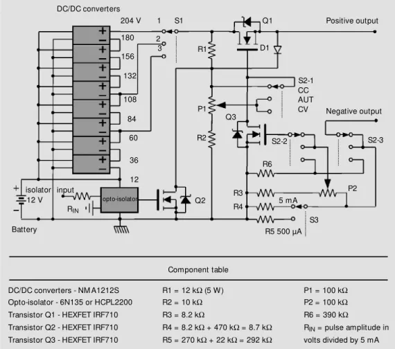
Figure 1 shows the complete electronic circuit. Eight DC/DC converters with 12-V inputs are connected in parallel to a battery. The 24-V outputs and the battery are con-nected in series to produce a 204-V total output. The circuit without the Q2 and Q3 transistors is a conventional regulated-volt-age power supply. In the absence of an input, Q2 transistor conducts with the on-state re-sistance close to 5 W, then its drain voltage to reference goes close to zero, turning off Q1. When a pulse is applied to the isolator input, the optically coupled signal turns off Q2 and this releases Q1, setting a voltage output which is determined by the position of the cursor in P1, less the small and practically constant gate/source polarization of Q1.
The scales of voltage, 5 to 50, 10 to 100 and 20 to 200 V, can be changed by switch-ing S1, takswitch-ing advantage of the fact that the
pick-up of the converters is adjusted in the P1 potentiometer.
When the input pulse ends, Q2 conducts again and this turns off Q1, ending the output pulse and discharging the capacitances asso-ciated with output through D1 and Q2.
The output pulse rise time is dependent on the time constant determined by the total Q2 drain/source capacitance and R1 resis-tance, since P1 plus R2 is much higher than R1. With a small R1, the rise time decreases at the expense of the power consumption. We adjusted R1 to a 5-µs rise time, which is 0.5% of the period of the fastest train of stimulation of practical importance on elec-trophysiology.
The Q3 circuit is a linear amplifier con-figured to work as a current stabilizer. It controls the output voltage to keep the level of current adjusted in the P2 potentiometer constant. This, in addition to permitting the isolator to operate in the current mode, pro-tects against output short circuits.
The isolator offers two ranges of current selected at the S3 switch. With S3 in the down position the range is from 50 to 500 µA. In the up position (see Figure 1) the range is from 0.5 to 5.0 mA.
All the controls are active in the auto-matic mode. The experimenter may adjust either voltage or current according to his requirements.
This isolator was designed to permit the use of a larger number of DC/DC converters with serial output connection (so as to in-crease the maximum voltage output), with-out the necessity of large circuit modifica-tion. These isolators may be connected with inputs in parallel or in different sources and the outputs may be connected in series to increase the voltage output or to shape wave-forms.
Although the factory parameters of the power transistors are not appropriate for this type of analysis (since they were intended for much larger currents) we will use them to evaluate the performance of the isolator (2). The output resistance in the voltage mode,
when Q3 is not active because the load cur-rent is not enough to keep it polarized, works like a non-stabilized voltage regulator. The output resistance of the source follower is reduced to the inverse of transconductance (3), so that:
Ro »1/gfs = 1 W
This very low resistance makes the isola-tor output closely approach a constant volt-age source, considering the much higher loads connected to the isolator output. The resistor structure for current control connected in series to the load taking the output resistance to the 1 kW range is still satisfactory. In the case of no voltage feedback, reference volt-age (voltvolt-age at P1 center tap) will directly reach output. In the last resource it is impor-tant that the voltage stability of the convert-ers maintains the assigned output voltage in
Component table
DC/DC converters - NM A1212S R1 = 12 kW (5 W) P1 = 100 kW
Opto-isolator - 6N135 or HCPL2200 R2 = 10 kW P2 = 100 kW
Transistor Q1 - HEXFET IRF710 R3 = 8.2 kW R6 = 390 kW
Transistor Q2 - HEXFET IRF710 R4 = 8.2 kW + 470 kW = 8.7 kW RIN = pulse amplitude in
Transistor Q3 - HEXFET IRF710 R5 = 270 kW + 22 kW = 292 kW volts divided by 5 mA
Figure 1 - HEXFET pow er stimu-lus isolator circuit. S1, position 1: 20 to 200 V; position 2: 10 to 100 V; position 3: 5 to 50 V. S3, position 1: 0.5 to 5 mA; position 2: 50 to 500 µA. CC, Constant current; AUT, automatic; CV, constant voltage.
S2-3 Negative output Positive output DC/DC converters
204 V 1 S1 Q1
D1 R1
S2-1 180
156
132
108
84
60
36
12 2
3
P1
R2
Q2
CC AUT CV
S2-2
R6
R3
R4
S3 R5 500 µA
P2 5 mA
opto-isolator input
isolator 12 V
Battery
RIN
all the current range of the isolator. With pulse output low, in the worst case, the cur-rent drain does not reach half of the nominal converter output current.
In the constant current mode, with the Q3 transistor amplifier working, the feedback loop is closed. In this condition the feedback loop multiplies the output resistance by the desensitization factor, so that:
Ro = (1 + ß.A)
where ß = 1 and A = gfs . RL (Q3 amplifier gain).
With 0.5 mA output, Ro without feed-back is close to 8 kW and the effective RL is R1 (12 kW), and thus the output resistance value should be Rof @ ß . A . Ro = 1 x 1.2 x 104 x 8 x 103 @
100 MW. In the other range the value increases 10 times, permitting output resistances of 1000 MW, which can keep current approximately constant with 100-MW intracellular microelectrodes.
The isolator performance parameters are suitable for intracellular and extracellular electrophysiological stimulation (4,5) and comparable to other commercially available stimulus isolation units (6,7).
To test a prototype of the stimulus isola-tor, after connecting the two grounds, shown in the figure connected to the opto-isolator, the procedure described below should be followed.
Start with no voltage connected to the input of the opto-isolator, measuring the DC voltages at the three positions of the S1 switch with a multimeter. This measurement indicates the state of the DC/DC converters. If the expected voltages (204, 108 and 60 V) are not found, check the converters individu-ally. The voltage at the center tap of the P1 potentiometer as well as at the positive out-put should be close to zero, when as referred to ground, independent of any external con-trol. The opto-isolator output should be 4 V above ground and the drain voltage from Q1 to ground should be close to zero.
Connect a positive DC source to the
opto-isolator input with a voltage which should be RIN . 5 mA as specified in the component table in the figure, and the coupler output should be close to zero. In the CV mode measure the voltage variation from P1 center tap and from the positive output, as referred to ground for all the three output voltage ranges. Check if the output voltage ranges are correct and the voltage between them and the center tap of P1 are set close to 4 V. A static test of the control of current may be carried out. At the higher voltage range, with the P1 potentiometer set to the maxi-mum output and in the CC mode, set the range to 5 mA. With a 10 kW (1/2 W) load resistor, check the voltage output variation from 50 to 100 V, acting on P2 potentiom-eter. With another resistor in series increase the load to 20 kW and repeat the check. The measured voltage values should now double because the current range is maintained. Set the two resistors in parallel and the meas-ure should drop to half. Using 100-kW resis-tors, repeat the same procedure for the 500 µA range. The measurements should be re-peated.
In the CV mode with a 10-kW load the maximum voltage adjustment should be lim-ited to approximately 100 V, since R6 limits the current to 10 mA to protect against out-put short circuits.
Re fe re nce s
1. Brasil RO & Leal-Cardoso JH (1986). Isola-dor de estímulo para uso em eletrofisiolo-gia. Resumos da I Reunião Anual da Federação das Sociedades de Biologia Experimental, São Paulo, SP, August, 309. 2. Horow itz H (1989). The Art of Electronics. Cambridge University Press, New York.
3. M illman J & Grabel A (1987). M icroelec-tronics. M cGraw Hill Inc., New York. 4. Brow n PB, M axfield BW & M oraff H
(1973). Electronics for Neurobiologists. M assachusetts Institute of Technology, Cambridge, M A.
5. Strong P (1970). Biophysical M
easure-ments. Tektronics Inc., Beaverton, OR. 6. World Precision Instruments (1998).
In-ternational Laboratory Equipment Sale Catalog. Sarasota, FL.