Fred Lacerda Amorim
[email protected] Pontifical Catholic University of Parana – PUCPR Mechanical Engineering Graduate Program Rua Imaculada Conceição, 1155 Prado Velho80.215 901 Curitiba, PR, Brazil
Walter Lindolfo Weingaertner
[email protected] Federal University of Santa Catarina – UFSC Mechanical Engineering Graduate ProgramCampus Universitário Trindade 80.040 970 Florianópolis, SC, Brazil
Irionson Antonio Bassani
[email protected] Pontifical Catholic University of Parana – PUCPR Department of Mechanical Engineering Rua Imaculada Conceição, 1155 Prado Velho 80.215 901 Curitiba, PR, BrazilAspects on the Optimization of
Die-Sinking EDM of Tungsten
Carbide-Cobalt
At present, due to their properties, the tungsten carbide-cobalt (WC-Co) composite materials are in huge demand by industry to manufacture special tools, dies/molds and components under erosion. The powder metallurgy is the usual process applied to obtain WC-Co products, but in some cases this process is unable to produce tools of very complex shapes and highly intricate details. Thus, additional conventional and non-conventional machining processes are required. In this context, the electrical discharge machining (EDM) is an efficient alternative process. However, the EDM parameters have to be properly set for any different tungsten carbide-cobalt composition and electrode material to achieve an appropriate level of machining performance. In this work, a special grade of tungsten carbide-cobalt was used as workpiece and a copper-tungsten alloy as electrode. Experiments on important EDM electrical and non-electrical parameter settings with reference to material removal rate, electrode wear ratio and surface roughness were carried out under typical rough and finish machining. This paper contributes with an attempt to provide insightful guidelines to optimize electrical discharge machining of WC-Co composite materials using CuW alloy electrodes.
Keywords: electrical discharge machining, tungsten carbide-cobalt, optimization guidelines
Introduction
1
Electrical discharge machining, generally known as EDM, is a thermoelectric process of non-conventional machining, where electrical discharges occur between two electrodes immersed in a dielectric fluid promoting heating, vaporization and removal of material. In EDM there are no physical cutting forces between the electrode and the workpiece; avoiding mechanical stresses, chatter and vibrations during machining, as reported by Kunieda et al. (2005). For that reason, EDM is widely applied to machine very complex shapes with high accuracy in hard materials.
Presently, as shown by Byrne et al. (2003), the tungsten carbide (WC) and its composites (WC-Co) is in huge demand by industry to manufacture different kinds of special tools, dies/molds and components under erosion; due to their properties of high compressive strength, hardness and resistance to wear over a large range of temperatures. As Dreyer et al. (1999) stated the powder metallurgy is the usual process for obtaining WC-Co products. In this process powder raw material is compacted and sintered to the shape of the product. But, in several cases the powder metallurgy is unable to produce some complex shapes with high accuracy in WC-Co composite materials. This leads to the need of applying other processes to reach the final quality required to the product.
Mahdavinejad and Mahdavinejad (2005) reported that some conventional machining processes can be used to machine these materials. Efforts have been done with CBN cutting tools, but the results have shown limited success due to the high hardness of WC-Co composite materials, combined with small and intricate geometry of the workpieces. They also mention that, when high accuracy in various kinds of cemented carbides is needed, the only process of conventional machining generally accepted is grinding. However, micro-cracks are produced on the workpiece surface due to the high temperatures generated during machining. Consequently, additional finish operations become necessary to eliminate these cracks and to achieve the final workpiece accuracy.
Kulkarni et al. (2002) reported that, among other non-conventional machining processes, electro-chemical machining
Paper accepted March, 2010. Technical Editor: Anselmo Eduardo Diniz
(ECM) and electrical discharge machining (EDM) are alternative processes that can be used to machine WC-Co composite materials with high accuracy and intricate geometries. On the other hand, Watson and Freer (1980) remarked that ECM produces a resistant oxide layer on the workpiece surface promoting very slow material removal rate; which is further decreased when high cobalt percentage is used in the alloy.
In this context, Jahan et al. (2009) pointed out that the EDM technology has been advancing as a promising process to manufacture high precision products in WC-Co composite materials. Lee and Li (2003) investigated the surface integrity of WC samples machined by EDM and remarked that the electrical discharge machining of diverse kinds of WC-Co materials regarding optimized parameters using different electrode materials is rather lacking deep investigation. This observation is in line with the work of Ho and Newman (2003) about the state of the art in EDM, where they showed that a significant number of recent researches are still focused in improving EDM performance measures such as material removal rate, electrode wear rate and surface integrity. Abbas et al. (2007) also reviewed the current research trends in EDM and pointed out that throughout the last decades many researchers have carried out theoretical and experimental tests aiming to optimize the EDM electrical and non-electrical variables for many kinds of workpiece and electrode materials.
Therefore, in the present study, a detailed sequence of optimization experiments with reference to important EDM electrical and non-electrical variables on machining of tungsten carbide-cobalt (WC-Co) using copper-tungsten alloy (CuW) electrode was carried out. Three important machining characteristics regarding the EDM performance were investigated. The first one is the material removal rate Vw, which means the volume of material
removed from the workpiece per minute. The second is the volumetric relative wear ϑ that corresponds to the ratio between the tool electrode wear rate Ve and the material removal rate Vw. The
third characteristic is the average surface roughness Ra.Accordingly,
Nomenclature
îe = discharge current, A t0 = pulse interval time, μs pin = dielectric inlet pressure, Pa td = ignition delay time, μs te = discharge duration, μs ti =pulse duration, μs tp = pulse cycle time, μs ue = discharge voltage, V ûi = open circuit voltage, V Ve = electrode wear rate, mm3/min Vw = material removal rate, mm3/min We = discharge energy, J
Greek Symbols
τ = duty factor
ϑ = volumetric relative wear
Some Theoretical EDM Background
This section presents information related to EDM material removal mechanism in order to enlarge the understanding of the experimental methodology proposed in this study. From investigations of DiBitonto et al. (1989), Mukund et al. (1989), Eubank et al. (1993), König and Klocke (1997), Kunieda et al. (2005), and many other researchers, the material removal in electrical discharge machining is associated with the erosive effect produced when spatially and discrete discharges occur between two electrical conductive materials. Sparks of short duration, ranging from 0.1 to 4000µs, are generated in a liquid dielectric working gap separating the electrode and the workpiece (10-1000 µm). The discharge energy We ≈ ue.ie.te [J] released by the generator is
responsible for melting a small quantity of material of both electrode and workpiece by conduction heat transfer. Subsequently, at the end of the pulse duration, a pause time begins and the melted pools are removed by forces which can be of electric, hydrodynamic, thermodynamic and spalling nature.
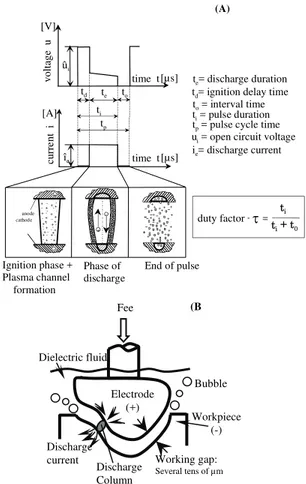
Figure 1(A) briefly presents the phases of a discharge in EDM process and Fig. 1(B) shows the concept of EDM. The first phase is the ignition phase which represents the lapse corresponding to the occurrence of the breakdown of the high open circuit voltage ûi
applied across the working gap until the fairly low discharge voltage
ue, which normally ranges from 10 to 40 V. This period is known as
ignition delay time td[μs]. The second phase, which instantaneously
occurs right after the first one when the current rapidly increases to the discharge current îe [A], is the formation of a channel of plasma
surrounded by a vapor bubble. The third phase is the discharge phase, when the channel of plasma of high energy and pressure is sustained for a period of time te [μs] causing melting and
evaporation of a small amount of material in both electrode and workpiece. The fourth, and last phase, is the collapse of the channel of plasma caused by turning off the electric energy, which causes the molten material to be violently ejected. At this time, known as interval time to [μs], a part of the molten and vaporized material is
flushed away by the flow of the dielectric fluid across the gap and the rest is solidified in the recently formed crater and surroundings. During the interval time to, it also occurs cooling of
electrode/workpiece and de-ionization of the working gap, necessary to promote an adequate dispersion of successive discharges along the surfaces of the electrode and the workpiece. This process continues until the geometry of the part is completed.
cur
re
n
t
i
volt
age
u
tp
ti
to
time t te
td
ûi
îe
[µs] [A]
[V]
duty factor- =
ti
ti
te= discharge duration
td= ignition delay time
to = interval time
ti = pulse duration
tp = pulse cycle time
τ
+ t0
ui = open circuit voltage
ie= discharge current
time t [µs]
-+ +
-+
-+-+ -+-+ +-+ -- + +
+ + --+- +
-+ -+ + -+ - -+
+ -+ +
-anode cathode
Ignition phase + Plasma channel formation
Phase of discharge
End of pulse
-+
+ + + + +
+ + + + +
+ + + + +
+ + + + ++
+ + + +
(A)
Workpiece (-) Dielectric fluid
Fee
Electrode (+)
Working gap:
Several tens of µm
Discharge Column Discharge current
(B
Bubble
Figure 1. (A) Schematic representation of the phases of an electric discharge in EDM and the definition of duty factor τ and (B) the concept of EDM phenomenon.
Considering the aforementioned EDM phenomenon, an asymmetric material removal of the electrode and the workpiece can be achieved by the appropriate choice of electrical parameters, electrode polarity, type of working gap flushing, planetary movement of the electrode and thermophysical properties of electrode/workpiece materials. According to Amorim & Weingaertner (2002), another EDM variable strictly associated to the electrical parameters and that influences on the machining characteristics is the duty factor τ, illustrated in Fig. 1. The duty factor can affect the material removal rate Vw, the volumetric
relative wear ϑ and the workpiece surface roughness Ra.
The duty factor τis the ratio between the pulse duration ti and
the pulse cycle time tp (ti + to). The value of duty factor τ should be
chosen as high as possible. The usual procedure to increase the value of τ is done by reducing the pulse interval time to and keeping
the pulse duration ticonstant. This procedure leads to the increase of
discharge frequencies promoting better rates of Vw and lower values
of ϑ. An important aspect regarding the choice of high values of τ is associated with the elevation of the contamination concentrated in the working gap. According to Schumacher (1990), some concentration of sub-microscopic particles, fibers or moisture drops in the working gap can reduce the ignition delay time td. It happens
because these particles arrange themselves in such a way that a kind of a bridge occurs intensifying the electric field. This then quickly fires another discharge. On the other hand, very high values of duty factor τ is responsible to promote many short-circuits, and arc-discharges causing low values of Vw and high levels of ϑ.
In current practice of EDM of metal alloys conservative decisions are taken to gain safer machining performance as stated by Wang et al. (1995). This means the use of duty factor τ = 0.5 (ti = to) in order to avoid short-circuit, arc-discharges and good
flushing conditions. For duty factor higher than 0.5 (ti > to) the
machining conditions might become worse and arcing damages can occur. Values of duty factor lower than 0.5 (ti < to) lead to low
machining rate.
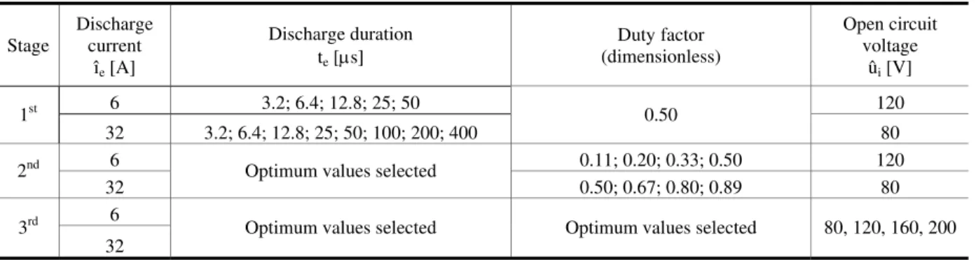
The respectively determined duty factors τ are then 0.11; 0.20; 0.33; 0.5 for finish machining and 0.5; 0.67; 0.8; 0.89 for the rough machining.
Experimental Methodology
In this work, a progression of experiments on the electrical discharge machining of a special grade of tungsten carbide-cobalt using copper-tungsten electrodes under rough and finish process conditions was performed. The tests were designed to adequately assess the effects of the input EDM independent parameters namely discharge current ie, discharge duration te, open circuit voltage ui
and duty factor τ on the EDM output dependent machining characteristics material removal rate Vw, volumetric relative wear ϑ
and workpiece surface roughness Ra. The discharge currents adopted
in here represent typical values for rough and finish EDMachining.
Experimental Procedure
The optimization of EDM machining characteristics was carried out into three stages. The range of the variables to perform the experiments is shown in Table 1. The implemented sequence for each stage is described as follows:
First Stage – Effect of Discharge Duration (te): as reported by Masuzawa (2001), the discharge energy We≈ ue.ie.te [J] induced in
the working gap is the main EDM factor responsible for the process performance, i.e., removal rate, electrode wear and surface integrity. Thus, at the first stage of this work, the value of duty factor τ is fixed at 0.5 and the machining characteristics is optimized against the variation of discharge duration te. Rough and finish machining
regimes are analyzed for discharge currents ie of 32 A and 6 A,
under an open circuit voltage ui, respectively at 80 V and 120 V.
The range of discharge duration te varies from 3.2 to 50 µs for the
finish machining and for EDM under the rough machining, te goes
up to 400 µs.
Second Stage – Effect of Duty Factor (τ): here the optimum discharge duration te that promoted the best machining characteristics
is kept constant and the values of pulse interval time to are modified.
This promotes the variation of the duty factor τ in order to further improve the machining performance. The range of the interval time t0
was specified as 100; 50; 25; 12,8 µs for the finishing machining and for the rough machining as 200; 100; 50; 25 µs.
Third Stage – Effect of Open Circuit Voltage (ûi): the variable (ûi)considerably affects the working gap size. Consequently, the open
circuit voltage ûi has to be properly set to guarantee a proper
dispersion of the sparks along the frontal area of the pair electrode/workpiece and to provide good flushing conditions. Now at the last stage, using the best discharge duration teand the most
appropriate duty factor τ obtained in stage two, the open circuit voltage ui is scanned from 80 to 200 V to verify its influence over
the EDM machining performance under rough and finish regimes.
Materials and Equipment
(i) Workpiece: square samples of tungsten carbide-cobalt 20 mm wide and 10 mm depth with Ra = 0.8 μm on the surface to be
machined were prepared by Wire EDM. The chemical composition of the WC-Co composite material is as follows: 88.2% of WC, 11.5% of Co+Ni and 0.3% of impurities. The WC average grain size is 2.0 µm, considered as fine grain size. This alloy has 14.30 g/cm3 of density, 1240 HV10 hardness, 2597°C of melting point and 420 kgf/mm2 of compressive strength. Figure 2 shows a scanning electron microscope (SEM) image of WC grains and the Co substrate of the WC-Co workpiece used in this work.
Figure 2. SEM image of the surface of tungsten carbide-cobalt workpiece.
Table 1. Stages and electrical and non-electrical parameters values for the optimization tests.
Stage
Discharge current
îe [A]
Discharge duration te [μs]
Duty factor (dimensionless)
Open circuit voltage
ûi [V]
6 3.2; 6.4; 12.8; 25; 50 120
1st
32 3.2; 6.4; 12.8; 25; 50; 100; 200; 400 0.50 80
6 0.11; 0.20; 0.33; 0.50 120
2nd
32 Optimum values selected 0.50; 0.67; 0.80; 0.89 80 6
3rd
32
(ii) Electrode: copper-tungsten (CuW) alloy cylindrical bars with 10 mm diameter and 100 mm length under negative polarity having chemical composition containing 70% of tungsten and 30% of copper were mounted axially within WC-Co workpiece, as shown in Fig. 3. The properties of CuW electrodes used in this work are the following: hardness of 37 HRC, melting point of 3500°C and density of 12.6 g/cm3.
CuW electrode
WC-Co workpiece CuW electrode
WC-Co workpiece
Figure 3. Assembly of WC electrode and WC-Co workpiece at the EDM machine tool.
(iii) Machine tool: a Charmilles ROBOFORM 30 CNC die-sinking machine tool, equipped with an isoenergetic generator that allows setting the value of discharge duration te was used throughout
the experiments. An important parameter is the ignition delay time
td. The time td elapses between applying the open circuit voltage ûi
across the gap until the discharge current îe is established. When
finish EDMachining is carried out longer times of td are applied. In
this work, td is set as 30% of discharge duration te for finish
machining. For rough EDMachining operations lower times of td are
used because the working gap is normally large. Here td is set to be
15% of discharge duration te. These values of td were established
based on pilot tests results.
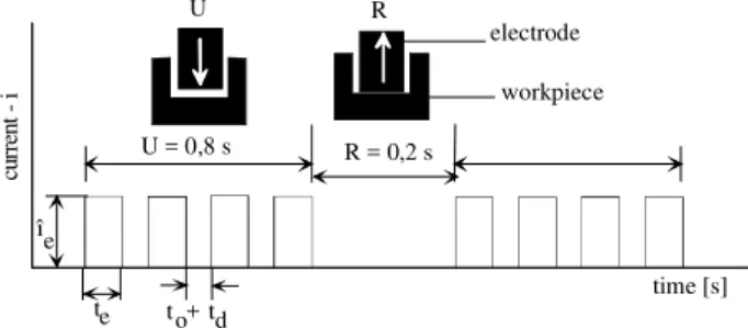
(iv) Flushing method: a hydrocarbon dielectric fluid with 3 cSt at 40°C, flash point of 134°C and 0.01 wt.% of aromatic contents were used for the tests. In this work shallow cavities of small diameter were planned to be machined. For that reason, a jet of dielectric fluid directly against the gap and the immersion of the pair electrode/workpiece into the dielectric were applied as flushing technique. This method was sufficient to evacuate the excess of eroded particles away from the working gap as well as to promote adequate cooling. In order to further improve the flushing efficiency, an alternation between periods of machining U [s] and periods of electrode retraction with no discharges R [s] was introduced, as shown in Fig. 4. The values of U and R were defined after pilot tests.
cur
rent
i
te to + td î
e
electrode
workpiece
time [s]
U = 0,8 s R = 0,2 s
U R
Figure 4. Series of pulses U [s] followed by a pause time R [s].
Results and Discussion
The objective of this study is to provide guidelines to optimize the EDM of tungsten carbide-cobalt using copper-tungsten electrodes under rough and finish machining. In order to achieve this target the experiments were carried out into three stages. The first stage deals with the variation of discharge duration te, the
second aims at using the best results of the first stage to analyze the influence of duty factor τ and the last stage concerns the influence of the open circuit voltage ui.
First Stage – Effect of Discharge Duration t
eThe discharge energy We ≈ ue.ie.te [J] induced in the working
gap is the main EDM factor responsible by the process performance,
i.e., removal rate, electrode wear and surface integrity. Thus, the discharge currents ie = 6 and 32 A were chosen to analyze the EDM
behavior under finish and rough machining conditions over the variation of discharge duration te. The initial value of duty factor τ =
0.5 was established because good EDM process stability is promoted.
The results of the material removal rate Vw against the variation
of discharge duration tefor negative copper-tungsten electrode are
summarized in Fig. 5. The global values of Vw for the discharge
current îe = 32 A are much higher than those achieved for îe = 6 A.
This occurs because the material removal rate Vw is dependent on
the energy We [J] released into the working gap, i.e., the increase of
discharge current ieleads to higher values of Vw. Here, the spalling
phenomenon, which consists of the separation of small volumes of WC ceramic phase from the base material, is also responsible for this behavior. The spalling effect is more prominent with the increase of discharge current, in that case causing an easier separation of small volumes of WC material promoting higher values of Vw. This spalling effect has been also observed in the
study of Lawers et al. (2005), with electrical discharge machining Si3N4-based ceramic material with addition of conductive phases.
Additionally, it can be noticed that as the discharge duration te
increases, regardless of the value of discharge current ie, the rate Vw
also increases up to a maximum value for a specific optimum te. The
highest material removal rate Vw is of approximately 4.2 mm³/min
for îe = 32 A to the optimum te = 200 µs. After this point Vw starts to
decrease. It arises from longer discharge duration te that diminishes
the pressure and energy of the channel of plasma over the molten material of the electrode and the workpiece. As a consequence, process instability in the form of short circuits and arc-discharges takes place lowering the material removal rate Vw.
0,0 0,5 1,0 1,5 2,0 2,5 3,0 3,5 4,0 4,5
3,2 6,4 12,8 25 50 100 200 400
32 A 6 A
discharge duration te
m
at
eri
al
rem
o
va
l
ra
te
-
Vw
mm3
min
[ µs ]
negative electrode (-) duty factor = 0,5
τ
Figure 5. The results of material removal rate Vw against the variation of
discharge duration te.
Figure 5 also shows that for discharge current îe = 6 A the
variation of discharge duration te from 3.2 to 50 μs did not affect
significantly the material removal rate Vw. This is related to the
small working gap size, which hinders the total molten material to be properly expelled from the gap at the end of the discharge. Consequently, the molten and vaporized material solidifies in the recently formed crater and surroundings. The best value of
Vw= 0.5mm3/min for the discharge current ie = 6 A is achieved for
te = 12.8 μs.
The volumetric relative wear ϑ represents the ratio between the electrode wear rate Ve [mm3/min] to the workpiece material removal
rate Vw [mm
3
/min]. The results of ϑ [%] as a function of discharge duration tefor currents ie = 6 and 32 A are shown in Fig. 6. For
discharge current ie = 6 Aincreasing the discharge duration te, a
decrease of ϑ is observed, reaching a minimum of about 20% at the optimum te = 12.8 μs. It is also seen that the variation of discharge
duration te did not affect significantly the values of ϑfor the rough
machining with ie = 32 A. For this current ie the volumetric relative
wear ϑ presents a trend of 18% up to the optimum te = 200 μs.
0 5 10 15 20 25 30
%
3,2 6,4 12,8 25 50 100 200 400
discharge duration te [ µs ]
V
o
lu
m
et
ric
R
ela
tive w
ea
r ϑ
negative electrode (-) duty factor = 0,5
τ
32 A 6 A ie [ A ]
Figure 6. Volumetric relative wear ϑ against the variation of discharge duration te.
Independently of the discharge duration tethe enlargement of
discharge current (ie = 6 to 32 A) promoted lower volumetric
relative wear ϑ when machining with CuW electrode. This phenomenon comes from the CuW electrode chemical composition (30% Cu and 70% W). The elevated concentration of the element tungsten with high melting point (3410°C) promotes higher resistance of the electrode against the thermal wear degradation during machining. The result is less electrode wear rate Ve and
better material removal rate Vw, which causes a decrease of
volumetric relative wear ϑ (Ve/Vw) when the discharge current ie
increases. Figure 7 shows the results of the surface roughness Ra
versus the discharge duration te. The lowest Ra = 1.1 μm is reached
for the discharge current ie = 6 A and te = 3.2 μs. For ie = 6 A the
variation of discharge duration tefrom 3.2 to 50 μs did not affect
considerably the average surface roughness Ra. This has to do with
the small working gap that does not promote an adequate evacuation of the eroded particles, but instead accumulate them in the crater and surroundings. When machining with ie = 32 A it is detected an
increase of the surface roughness Ra as the discharge duration te is
raised. This is due to the higher values of material removal rate Vw
that produces deeper and larger craters on the surface of the workpiece.
0,0 0,5 1,0 1,5 2,0 2,5 3,0 3,5 4,0 4,5
3,2 6,4 12,8 25 50 100 200 400 32 A
ie [ A ]
negative electrode (-) duty factor = 0,5
τ
discharge duration te [ µs ]
S
urf
a
c
e
R
o
n
e
ss
R
a
µm
u
gh
6 A
Figure 7. Average surface roughness Ra against the variation of discharge
duration te.
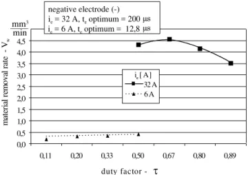
Second Stage – Effect of Duty Factor τ
From the optimized values of discharge duration te obtained in
stage one, the duty factor τ was varied to analyze its influence on the EDM performance. The duty factor τ of 0.5 was the starting point, as shown in Fig. 8. The optimum discharge duration teis kept fixed
and the interval time to is modified. From the best conditions for
finish machining (te = 12.8 µs, ie = 6 A) the duty factor τ is reduced
from 0.5 to 0.11 by increasing the interval time to within the range
of 12.8; 25; 50; 100 µs. It observed from Fig. 8 that this variation of duty factor τ does not affect significantly the values of material removal Vw.
For the discharge current ie = 32 A at the optimum discharge
duration te = 200 μs the duty factor τ is raised from 0.5 up to 0.89 by
lowering the interval time toat the sequence of 200, 100, 50, 25 µs.
It is noticed a little increase of the material removal rate Vw ≈ 4.5 mm3/min for the duty factor τ of 0.67. Higher values of
duty factor (τ = 0.8 and 0.89) reduces the material removal rate. This is caused by the low interval times to causing
over-concentration of debris in the working gap, which then brings instability into the working gap either in the form of arc discharge pulses or short-circuit pulses.
0,0 0,5 1,0 1,5 2,0 2,5 3,0 3,5 4,0 4,5
0,11 0,20 0,33 0,50 0,67 0,80 0,89
duty factor -
mm3
min
m
ateria
l r
em
o
v
al
rat
e
- V
w
τ
negative electrode (-) ie = 32 A, te optimum = 200 µs
ie = 6 A, te optimum = 12,8 µs
32 A 6 A ie [ A ]
Figure 8. The results of material removal rate Vw against the variation of
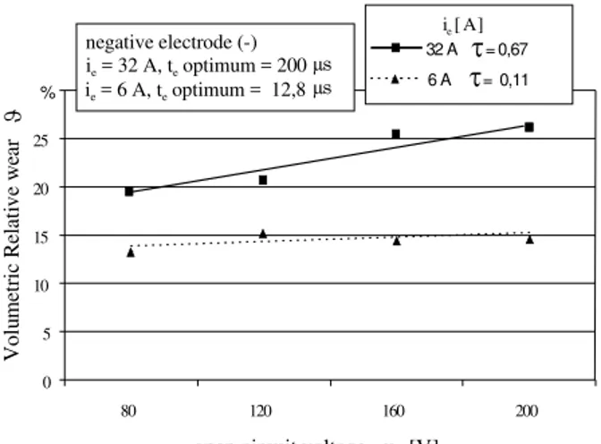
Figure 9 shows that for both rough and finish machining (ie =
32 and 6 A) the variation of duty factor τ significantly influences the values of volumetric relative wear (ϑ = Ve/Vw). For the discharge
current ie = 32 A the increase of duty factor τ from 0.5 to 0.89
promotes an elevation of the volumetric relative wear ϑ up to about 22%. This is due to the low interval times to that promote high
concentration of EDM byproducts in the working gap, reducing the material removal rate Vw. For the finish machining the decrease of
duty factor τ from 0.5 to 0.11 reduces the volumetric relative (ϑ = Ve/Vw). Here it occurs because longer interval times to improve the
flushing conditions by reducing the occurrence of arc-discharges and short-circuits promoting more stability to the machining.
0 5 10 15 20
0,11 0,20 0,33 0,50 0,67 0,80 0,89
%
Vo
lu
m
etr
ic
R
el
ati
ve
w
ea
r ϑ
duty factor -
τ
32 A6 A
negative electrode (-) ie = 32 A, te optimum = 200 µs
ie = 6 A, te optimum = 12,8 µs
Figure 9. Volumetric relative wear ϑVw against the variation of the duty
factor τ.
From Fig. 10 it is clearly seen that the surface roughness for rough machining is not extensively affected by the variation of the duty factor τ, remaining at about Ra = 3.5 μm. This has to do with the fact
that the duty factor was varied by the modification of the interval time to, which does not influence on the energy We = ie.ue.te [J] supplied to
the machining process. For finish machining, the reduction of duty factor from 0.5 to 0.11 caused insignificantly decrease on the surface roughness Ra from 1.5 to approximately 1.2 μm.
0,0 0,5 1,0 1,5 2,0 2,5 3,0 3,5
0,11 0,20 0,33 0,50 0,67 0,80 0,89 duty factor
τ
S
u
rfa
c
e
R
o
u
g
h
ne
ss
R
a
µm
32 A 6 A
ie [ A ] negative electrode (-)
ie = 32 A, te optimum = 200 µs
ie = 6 A, te optimum = 12,8 µs
Figure 10. The results of surface roughness Ra against the variation of the duty factor τ.
Third Stage – Effect of Open Circuit Voltage u
iFigure 11 shows the influence of the variation of the open circuit voltage ui on the results of material removal rate Vw for the
EDMachining of tungsten carbide-cobalt composite material. For the rough machining with ie = 32 A, duty factor τ = 0.67 and
optimum te = 200 μs, the variation of the open circuit (ui = 80 to
200 V) provides a little raise on the value of Vw to 5.2 mm3/min.
This is due to the intrinsic relation of the open circuit voltage ûi
with the size of the working gap, i.e., the distance between the electrode and the workpiece during the electric discharge occurrence. For the rough EDM conditions (ie = 32 A) higher
values of ûi give support to the occurrence of larger working gaps.
This fact promotes enhancement of flushing of the eroded particles away from the working gap causing an improvement of the material removal rate Vw.
From Fig. 11 it is observed that, for finish machining with ie = 6
A under the optimum electrical parameters, the variation of the open circuit voltage ui does not affect the results of material removal rate
Vw. This happens because the variation of ui from 80 to 200 V does
not widen the working gap so that the flushing conditions could be improved to provide better values for the material removal rate Vw.
0,0 1,0 2,0 3,0 4,0 5,0
80 120 160 200
32 A = 0,67 6 A = 0,11
open circuit voltage - ui [V]
m
ateria
l re
m
o
v
al rate
- V
w
mm3 min
τ
τ
negative electrode (-) ie = 32 A, te optimum = 200 µs
ie = 6 A, te optimum = 12,8 µs
ie [ A ]
Figure 11. Material removal rate Vw against the variation of the open circuit voltage ui.
Figure 12 presents the results of volumetric relative wear ϑ for the variation of open circuit voltage ui. In EDM the very small
byproducts generated by the dielectric burning tends to adhere over the surface of the electrode promoting the formation of a protective layer against the wear. These byproducts’ concentration in the working gap depends on its size, i.e., the larger the working gap the easier the byproducts are removed by the flushing. For rough machining with ie = 32 A, the increase of ui provided a working gap
growth causing better flushing conditions, which then lowered the concentration of the byproducts. This has prevented the formation of the protective layer on the surface of the electrode causing an increase of the values of electrode wear rate Ve. As a consequence,
the volumetric relative (ϑ = Ve/Vw) is increased when the open
circuit voltage varies from 80 to 200 V. For the finish machining (ie = 6 A) the variation of ui did not affect the values of the
volumetric relative wear.
Figure 13 shows that the elevation of the open circuit voltage ui
for the rough machining with ie = 32 A increased considerably the
surface roughness Ra from about 3.2 to 5.5 μm. This takes place
because the variation of ui raised the material removal rate Vw
promoting deeper and larger craters on the surface of the tungsten carbide-cobalt workpiece. For finish machining (ie = 6 A) it is
observed that the levels of the surface roughness Ra is not
influenced by the different values of the open circuit voltage ui.
0 5 10 15 20 25
80 120 160 200
open circuit voltage - ui [V]
%
V
o
lu
m
etr
ic
R
el
ati
ve
w
ear
ϑ
32 A = 0,67 6 A = 0,11
τ
τ
ie [ A ]
negative electrode (-) ie = 32 A, te optimum = 200 µs
ie = 6 A, te optimum = 12,8 µs
Figure 12. Volumetric relative wear ϑ against the variation of the open circuit voltage ui.
0,0 1,0 2,0 3,0 4,0 5,0
80 120 160 200
open circuit voltage - ui [V]
Su
rf
a
c
e
R
ou
g
h
n
e
ss
R
a
µm
32 A = 0,67 6 A = 0,11
τ
τ
ie [ A ]
negative electrode (-) ie = 32 A, te optimum = 200 µs
ie = 6 A, te optimum = 12,8 µs
Figure 13. Results of surface roughness Ra against the variation of the open circuit voltage ui.
Conclusion
In EDM some major tasks concern achieving high material removal rate, small electrode wear and low surface roughness. Thus, in this work, a sequence of experiments were performed to provide useful guidelines to optimize the die-sinking EDM of tungsten carbide-cobalt (WC-Co) using copper-tungsten (CuW) electrode under rough and finish regimes. Important EDM parameters were investigated with reference to the workpiece material removal rate
Vw, the volumetric relative wear ϑ and the average surface
roughness Ra. From the experimental investigations the following
conclusions can be drawn:
(i) The increase of discharge duration te promotes higher
material removal rate Vw and produces poorer surface texture Ra for
rough machining regimes, but does not affect considerably the values of Vw and Ra for finish machining. The volumetric relative
wear ϑ reduces with the increase of te for finish machining, but is
not affected for rough machining regime.
(ii) The variation of the duty factor τ slightly improves the material removal rate Vw for the both rough or finish machining
regimes. The surface texture Ra is not affected significantly by the
variation of the duty factor τ. The volumetric relative wear ϑ for rough and finish regimes is significantly influenced by the variation of the values of the duty factor.
(iii) The open circuit voltage ui increases the material removal
rate Vw and the surface texture Ra for rough machining regime. For
finish machining the values of Vw and Ra does not change with the
variation of the open circuit voltage ui. The volumetric relative wear
ϑ for rough machining gets higher with the rise of the open circuit voltage ui,but its values for finish regime are not affected.
References
Abbas, N.M., Solomon, D.G. and Bahari, M.F., 2007, “A review on current research trends in electrical discharge machining (EDM)”,
International Journal of Machine Tools and Manufacture, Vol. 47, pp. 1214-1228.
Amorim, F.L., Weingaertner, W.L., 2002, “Influence of Duty Factor on the Die-Sinking Electrical Discharge Machining of High-Strength Aluminum Alloy under Rough Machining”, Journal of the Brazilian Society of Mechanical Sciences, Vol. 24, pp. 194-199.
Byrne, G., Dornfeld, D. and Denkena, B., 2003, “Advancing Cutting Technology”, CIRP Annals – Manufacturing Technology, Vol. 52, No. 2, pp. 483-507.
DiBitonto, D.D., Eubank, P.T., Patel, M.R. and Barrufet, M.A., 1989, “Theoretical models of the electrical discharge machining process I: a simple cathode erosion model”, Journal of Applied Physics, Vol. 66, No. 9, pp. 4095-4103.
Dreyer, K., Westphal, H., Sottke, V. and Tabersky, R., 1999, “New Developments for Hardmetals, Cermets and Coatings in Experiment and Practice”, VDI-Seminar: High Performance Processes in Cutting Operations, Oct. 26-27, Dortmund.
Eubank, P.T., Patel, M.R., Barrufet, M.A. and Bozkurt, B., 1993, “Theoretical models of the electrical discharge machining process III: the variable mass, cylindrical plasma model”, Journal of Applied Physics, Vol. 73, No. 11, pp. 7900-7909.
Ho, K.H. and Newman, S.T., 2003, “State of the art electrical discharge machining (EDM)”, International Journal of Machine Tools & Manufacture, Vol. 43, pp. 1287-1300.
Jahan, M.P., Wong, Y.S., Rahman, M., 2009, “A study on the fine-finish die-sinking micro-EDM of tungsten carbide using different electrode materials”,
Journal of Materials Processing Technology, Vol. 209, pp. 3956-3967.
König, W. and Klocke, F., 1997, “Fertigungsverfahren – 3: Abtragen und Generieren”, Berlin, Springer, Vol. 3.
Klocke, F., Karden, A., 1999, “Material Characteristics after Cavity Sinking by EDM. Production Engineering”, Vol. 6, No. 2, pp. 35-38.
Kulkarni, A., Sharan, R., Lal, G.K., 2002, “An experimental study of discharge mechanism in electrochemical discharge machining”, International Journal of Machine Tools and Manufacture, Vol. 42, pp. 1122-1127.
Kunieda, M., Lauwers, B., Rajurkar, K.P. Schumacher, B.M., 2005, “Advancing EDM through fundamental insight into the process”, Annals of CIRP Manufacturing Technology, Vol. 54, N. 2, pp. 599-622.
Lee, S.H. and. Li, X.P, 2003, “Study on the surface integrity of the machined workpiece in the EDM of WC”, Journal of materials processing technology, Vol. 139 (1-3 SPEC), pp. 315-321.
Lawers, B., Kruth, J.P., Liu, W., Eeraerts, W., Schacht, B., Bleys, P., 2004, “Investigation of material removal mechanisms in EDM of composite ceramic materials”, Journal of Materials Processing Technology, Vol. 149, pp. 347-352.
Mahdavinejad, R.A. and Mahdavinejad, A., 2005, “ED machining of WC-Co”, Journal of materials processing technology, Vol. 162-163, pp. 637-643.
Masuzawa, T, 2001, “Micro-EDM”, Proceeding of 13th Symposium for
Electromachining – ISEM XIII, Vol. 1, pp. 3-18.
Mukund, R., Patel, M.A.B., Eubank, P.T., 1989, “Theoretical models of the electrical discharge machining process II: the anode erosion model”,
Journal of Applied Physics, Vol. 66, No. 9, pp. 4104-4111.
Schumacher, B.M., 1990, “About de role of debris in the gap during electrical discharge machining”, Annals of the CIRP Manufacturing Technology, Vol. 39, No. 1, pp. 197-190,
Wang, W.M., Rajurkar, K.P. and Akamatsu, K., 1995, “Digital Gap Monitor and Adaptive Integral Control for Auto-Jumping in EDM”, Journal of Engineering for Industry, Transactions of the ASME, Vol. 117, pp. 253-258.
Watson, S.H., Freer, H.E., 1980, “A comparative study of electro-chemical and electro discharge machining of a tungsten carbide 25% Cobalt alloy”, Proceedings of 6th Symposium for Electro-Machining, ISEM VI, Vol. 6,