SELF-‐HEATING ANALYSIS OF 1570 NM INGAASP BURIED TUNNEL JUNCTION
PHOTONIC CRYSTAL VCSEL
M. SABAGHI
Photonics and Quantum Technologies Research School, Nuclear Science and Technology Research Institute, Tehran, Iran [email protected] Received 18/11/2018 – Acepted 26/12/2018 DOI: 10.15628/holos.2018.7950 ABSTRACT
In this paper, the lattice temperature in an InP-‐based 1570 nm InGaAsP buried tunnel junction photonic crystal vertical-‐cavity surface-‐emitting laser (BTJ-‐PhC VCSEL) was varied between 280 K until 370 K and its effects on the characteristics of the device was investigated. The temperature profiles of the BTJ-‐PhC VCSEL are obtained iteratively by considering their temperature-‐dependent material properties and the spatial distribution of all the significant heat sources. The thermal resistance used to model the electrical contacts causes about 8 K temperature increment above the ambient temperature (300 k) at a bias of 3 V and a
10.865 % increase in the threshold current is observed with temperature increment. This paper provides key results of the device characteristics upon lattice temperature, including the light power versus electrical voltage, the threshold current versus temperature, the wall-‐plug efficiency and the differential quantum efficiency versus temperature. Furthermore, various elements of heat sources within the active region were analyzed upon the increment of lattice temperature. Results obtained from Silvaco ATLAS software based on the powerful effective frequency method.
KEYWORDS: Self-‐heating analysis, InGaAsP, Buried tunnel junction (BTJ), Photonic crystal (PhC), Vertical-‐cavity surface-‐emitting laser (VCSEL).
1. INTRODUCTION
The lasers are devices that radiate light through a procedure of optical amplification based on the stimulated emission of photons (Marjani, et al., 2011a; Marjani, et al., 2012; Marjani, et al., 2013; Mirzaei et al., 2016; Behrouzinia, et al., 2016; Deppe, et al., 2018). In recent decade, one of the serious research topics in high-‐performance optical communication systems is the vertical-‐cavity surface-‐emitting laser (VCSEL) where single mode operation, high-‐output power, high-‐speed modulation and low manufacture cost are necessary. Today, the important difficulties in emerging VCSELs are high optical gain of active area and high thermal conductivity of distributed Bragg reflector (Faez, et al., 2011; Marjani and Marjani, 2012b; Majdabadi, et al., 2014; Mehta, et al., 2018). Recently, researchers have manufactured an InP-‐based long
wavelength VCSELs capable of about 40 Gbit/sec modulation that has coplanar contact pads, low internal chip capacitance, reduced cavity length, and high single mode power (Khafaji, et al., 2018; Szilagyi, et al., 2018). On the one hand, increasing device heating is a serious problem for VCSELs for showing continuous waveform (CW) operation at room temperature due to the high threshold current densities. On the other hand, thermal modeling of VCSELs is essential in order to optimization (Marjani, et al., 2011b; Marjani, et al., 2011c; Marjani and Marjani, 2012a; Marjani, 2013).
Therefore, previous researchers presented thermal modeling of VCSELs with various levels of combined physics and self-‐consistency (Piprek, et al., 2000; Piprek, 2002; Streiff, et al., 2003; Rissons, et al., 2003; Qi, et al., 2010). Also, a coupled electro-‐opto-‐thermal VCSEL simulation model developed for moderate injection level below the thermal rollover condition of VCSEL (Streiff, et al., 2003). The carriers transfer energy mechanism to the crystal lattice causes the lattice heat. Since the thermal energy of the lattice rises, device temperature increases that limit the performance of VCSEL (Piprek, 2003). Heat sources including Joule heat, electron–hole recombination heat, Thomson heat and optical absorption heat.
In this paper, an accurate analysis of the thermal properties of 1570 nm InGaAsP buried tunnel junction photonic crystal vertical-‐cavity surface-‐emitting laser (BTJ-‐PhC VCSEL) is presented and investigated based on the powerful effective frequency method (Atlas – Device Simulation Framework., 2018). In this way, the temperature profile is calculated using the effective frequency method by considering all the important heat sources including Joule heat, electron–hole recombination heat, Thomson heat and optical absorption heat. The rest of this paper is described as follows: The numerical model and the details of the BTJ-‐PhC VCSEL structure are described in section 2. Section 3 provides the results and discussion. Finally, we conclude in section 4.
2. MODEL and DEVICE STRUCTURE
It is essential to consider the interaction of electrical, optical and thermal that occur during the device operation when modeling BTJ-‐PhC VCSEL. The fundamental equations are Poisson and continuity equations for electrons and holes, which link together. The Poisson's equation is defined as (Atlas – Device Simulation Framework., 2018):
(
ε ψ)
ρ
where ψ, ρ and ε are the electrostatic potential, local charge density and local permittivity, respectively. The continuity equations of electron and hole are defined by (Atlas – Device Simulation Framework., 2018): 1 . 1 . n n n p p p n G R J t q p G R J t q ∂ = − + ∇ ∂ ∂ = − + ∇ ∂ ur ur 2
where n, p, Jn, Jp, Gn, Gp Rn, Rp and q are the electron concentration, hole concentration, electron
current density, hole current density, electrons generation rate, holes generation rate, electrons recombination rate, holes recombination rate and magnitude of electron charge, respectively. The primary equations in modeling are Helmholtz equation, the photon rate equation and heat generation equation that derived from heat flow equation. The Helmholtz equation is solved to determine the transverse optical field profile and is defined as (Atlas – Device Simulation Framework., 2018): 2 0 2 ( , , ) ( , , , ) ( , , ) 0 E r z r z E r z c ω ϕ ε ϕ ω ϕ ∇ + = 3
where ω, ε(r, z, φ, ω), E(r, z, φ) and c are the frequency, the complex dielectric permittivity, the optical electric field and the speed of light in the vacuum.
The photon rate equation relates electrical and optical models and is defined as (Atlas – Device Simulation Framework., 2018):
1 ( ) m m m m m sp eff ph eff dS c cL G S R dt = N −τ −N + 4
where Sm, Gm, Rspm, L, Neff, τphm and c are the photon number, the modal gain, the modal
spontaneous emission rate, laser losses, the group effective refractive index, the modal photon lifetime and the speed of light in the vacuum. The m refers to modal number. The modal gain, modal of spontaneous emission rate and modal photon lifetime equations are defined as (Atlas – Device Simulation Framework., 2018):
(
)
(
)
(
)
2 0 , . , ( , ) 1 . m m m m m m m sp sp m a fc mir m lm ph G g r z E r z rd drdz R r r z rd drdz c c G NEFF NEFF θ θ α α α ω ν τ = = = + + = −∫∫∫
∫∫∫
5where Em(r, z), αa, αfc, αmir, vlm are the normalized optical field, bulk absorption losses, free-‐
carriers losses, mirrors losses and a parameter of dimensionless frequency, respectively. The heat flow equation is defined as (Atlas – Device Simulation Framework., 2018):
( ) L L T C T H t κ ∂ = ∇ ∇ + ∂ 6
where C, κ, H, TL and H are the heat capacitance per unit volume, the thermal conductivity the
generation, the local lattice temperature and the heat generation term, respectively. The heat generation equation is defined as (Atlas – Device Simulation Framework., 2018):
2 2 [ n p ] ( )[ ( )] ( ) p n L p n L n n p p n p J J H q R G T P P T J P J P q nµ qµ p φ φ = + + − − + − − ∇ + ∇ uuuuuuur uuuuuur uur uur 7
Where first, second and third term account for the Joule heating, the recombination and generation heating and cooling term; and the Peltier and Joule-‐Thomson effects, respectively.
The above-‐mentioned equations can account for the mutual dependence of electrical, thermal, optical and elements of heat sources. They are solved self-‐consistently together that the Helmholtz equation solution is effective frequency method based on the improved effective index model with Silvaco ATLAS software in the device design and optimization (Atlas – Device Simulation Framework., 2018). This model shows accuracy for the great portion of preliminary problems and therefore, it is very well adapted to modeling of VCSEL structures.
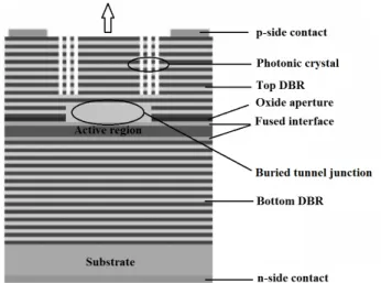
Figure. 1 shows the schematic structure of BTJ-‐PhC VCSEL device based on the recent experimental device (Piprek et al., 1997). The active region of BTJ-‐PhC VCSEL Includes from six quantum wells (QWs) with 5.5nm In0.76Ga0.24As0.82P0.18 and 8nm In0.48Ga0.52As0.82P0.18 as the well
and barrier, respectively. Also, there is InP and GaAs layers in both sides of this active region. The top distributed Bragg reflector of BTJ-‐PhC VCSEL Includes from 30 layers of GaAs/Al0.33Ga0.67As
with index of refraction of layers 3.38 and 3.05, respectively. In addition, the bottom distributed Bragg reflector of BTJ-‐PhC VCSEL Includes from 28 layers of GaAs/AlAs with index of refraction of layers 3.38 and 2.89, respectively. Above the active layers, the tunnel junction composed of a p++-‐
InGaAsP/n++-‐ InGaAsP is located. The tunnel junction is thin, and its layers bandgap is wider than
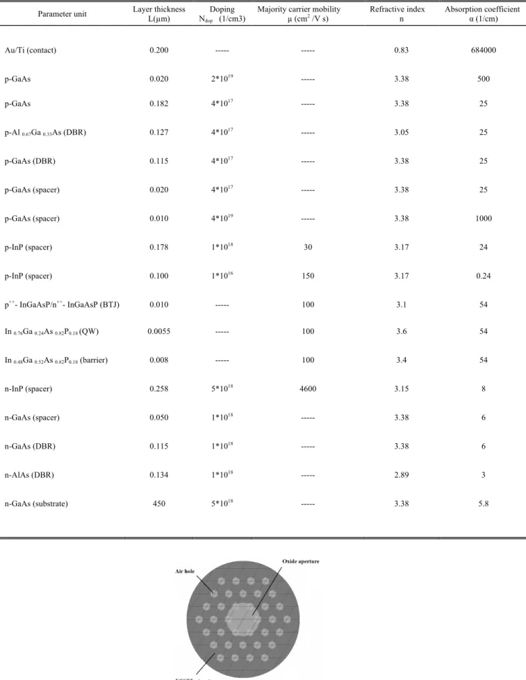
the bandgap of the QWs to avoid optical absorption. Further details of the BTJ-‐PhC VCSEL and all material parameters are given in Table I that including determined values from the experimental results (Piprek et al., 1997). On the other hand, the triangular-‐lattice air holes are formed in the top distributed Bragg reflector of BTJ-‐PhC VCSEL. As seen from Figure. 2, the optical confinement is achieved by seven air holes where the center is missed off to make the defect region.
Table.1: Physical parameters for BTJ-‐PhC VCSEL.
Parameter unit Layer thickness L(µm) N Doping dop (1/cm3)
Majority carrier mobility
µ (cm2 /V s) Refractive index n Absorption coefficient α (1/cm)
Au/Ti (contact) 0.200 --- --- 0.83 684000 p-GaAs 0.020 2*1019 --- 3.38 500 p-GaAs 0.182 4*1017 --- 3.38 25 p-Al 0.67Ga 0.33As (DBR) 0.127 4*1017 --- 3.05 25 p-GaAs (DBR) 0.115 4*1017 --- 3.38 25 p-GaAs (spacer) 0.020 4*1017 --- 3.38 25 p-GaAs (spacer) 0.010 4*1019 --- 3.38 1000 p-InP (spacer) 0.178 1*1018 30 3.17 24 p-InP (spacer) 0.100 1*1016 150 3.17 0.24 p++- InGaAsP/n++- InGaAsP (BTJ) 0.010 --- 100 3.1 54 In 0.76Ga 0.24As 0.82P0.18 (QW) 0.0055 --- 100 3.6 54 In 0.48Ga 0.52As 0.82P0.18 (barrier) 0.008 --- 100 3.4 54 n-InP (spacer) 0.258 5*1018 4600 3.15 8 n-GaAs (spacer) 0.050 1*1018 --- 3.38 6 n-GaAs (DBR) 0.115 1*1018 --- 3.38 6 n-AlAs (DBR) 0.134 1*1018 --- 2.89 3 n-GaAs (substrate) 450 5*1018 --- 3.38 5.8
3. RESULTS AND DISCUSSION
Heat loss of BTJ-‐PhC VCSEL is defined by means of thermal contacts at the top electrode, bottom electrode and the device sidewall. In order to modeling heat loss induced by the radiation from VCSEL device to the heatsink, it is used from the thermal contacts as the thermal conductivities.
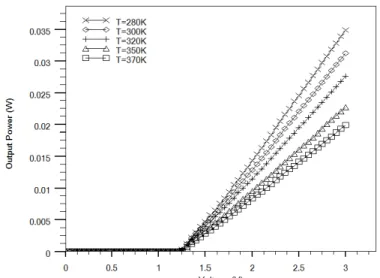
Figure. 3 and Figure. 4 show the output characteristics of BTJ-‐PhC VCSEL device in terms of light power versus electrical voltage and the current versus voltage with variation of the lattice temperature between 280 K until 370 K. As seen, the lattice temperature of BTJ-‐PhC VCSEL increases at higher voltages because of increasing in dark carrier recombination within the BTJ-‐ PhC VCSEL device.
Figure. 5 shows the plot for the optical gain of the BTJ-‐PhC VCSEL as a function of voltage for different lattice temperature. However, the small variation of the lattice temperature does not affect on the optical gain especially at higher voltages, as can be observed from Figure. 5.
Figure 3: The light power of the BTJ-‐PhCVCSEL as a function of electrical voltage for different lattice temperature.
Figure 4: The current of the BTJ-‐PhCVCSEL as a function of electrical voltage for different lattice temperature.
Figure. 6 displays the threshold current values of the BTJ-‐PhC VCSEL as a function of lattice temperature. Increase in the lattice temperature causes threshold current extremely increases that its value is 4.97 mA at 280 K up to 5.51 mA at 370 K, as can be confirmed in Figure. 6. It should be mainly due to expansion of the gain spectrum and the overflow of carriers in the hetero-‐barriers. On the other hand, the leakage currents or dark recombination processes are temperature-‐dependent that they cause the thermal rollover effect in the characteristics of BTJ-‐ PhC VCSEL (Ng et al., 2004).
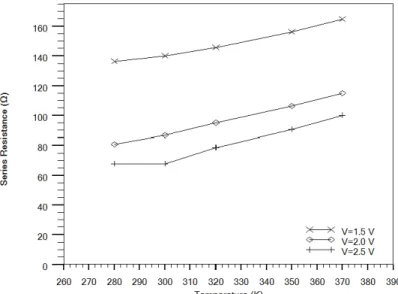
The series resistance of the BTJ-‐PhC VCSEL as a function of the lattice temperature is presented in the Figure. 7. As can be seen, the increasing of lattice temperature leads to a decrease in the the device series resistance. However, higher voltages assist in reducing the series resistance across the device, the output current is reduced at higher lattice temperatures. Since the wall-‐plug efficiency of VCSELs can be high even with relatively low input powers, the BTJ-‐PhC VCSEL VCSELs are attractive devices. The equations of wall-‐plug efficiency can be as
Figure 5: The optical gain of the BTJ-‐PhC VCSEL as a function of voltage for different lattice temperature.
Figure 7: The series resistance of the BTJ-‐PhC VCSEL as a function of the lattice temperature.
follows (Numai et al., 2004): out wp P IV η = 8
where Pout, I and V are the output optical power, the injection current and the bias voltage,
respectively.
The equations of differential quantum efficiency can be approximated into simple forms as follows (Numai et al., 2004):
D g dP 1 dI E η ≈ 9
where Eg is the bandgap energy.
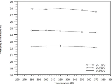
Figure. 8 and Figure. 9 show the efficiencies of BTJ-‐PhC VCSEL device in terms of the wall-‐ plug efficiency and the differential quantum efficiency versus the lattice temperature. As can be seen from Figure. 8 and Figure. 9., an increase in the lattice temperature lead to the decreasing of both the wall-‐plug efficiency and the differential quantum efficiency, which should be mainly due to the effects of Auger processes, valence band absorptions and free carrier absorptions. Because of the small conduction band offset between quantum well and barrier, the electrons leak out of the quantum wells into the barriers at high temperature. The electric field induced by the unbalanced charge distribution lead to trapping the holes in the barriers and increasing the absorption loss and recombination. As can be confirmed in Figure. 8 and Figure. 9., the wall-‐plug efficiency decreases with increasing operating voltage from 27.795 % at 1.5 V to 22.318 % at 2.5 V at 300 K; and the differential quantum efficiency increases with increasing operating voltage from 34.145 % at 1.5 V to 41.29 % at 2.5 V at 300 K.
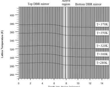
Figure. 10 and Figure. 11 illustrate the contour plots of the lattice temperature in the BTJ-‐ PhC VCSEL and the lattice temperature within a vertical cross-‐section of the BTJ-‐PhC VCSEL, respectively. The thermal resistance leads to an increase about 8 K of temperature of the BTJ-‐PhC
Figure 8: The wall-‐plug efficiency of the BTJ-‐PhCVCSEL device as a function of lattice temperature.
Figure 9: The differential quantum efficiency of the BTJ-‐PhCVCSEL device as a function of lattice temperature.
Figure 10: The contour plot of the lattice temperature in the BTJ-‐PhC VCSEL.
Figure 11: The lattice temperature within a vertical cross-‐section of the BTJ-‐PhC VCSEL.
VCSEL above the ambient temperature (300 k) at 3 V of the bias voltage, as shown in Figure. 10. Because of the lower refractive index of the top distributed Bragg reflector materials and consequently poor thermal conductivity, the peak of temperature is at the top distributed Bragg reflector region. The second highest and lowest temperature value of BTJ-‐PhC VCSEL structure are the multi quantum wells and the bottom distributed Bragg reflector region. As can be confirmed in Figure. 11, the lattice temperature of device increases gradually with surrounding temperature increment.
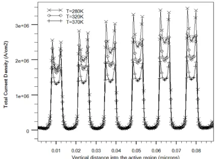
Figure. 12 demonstrates the Joule heat power within a vertical cross-‐section of the active region of BTJ-‐PhC VCSEL structure at 3 V of bias voltage. As seen, the lattice temperature increment lead to the reduction of the Joule heat power because of the lower current density, as shown in Figure. 13.
The Peltier-‐thomson heat transfers between carriers and lattice as current flows along a gradient of the thermoelectrical power. The most important effective parameters on the Peltier-‐
thomson heat are the density of states, carrier concentration, and temperature. The Peltier-‐ thomson heat power within a vertical cross-‐section of the active region of BTJ-‐PhC VCSEL structure at 3 V of bias voltage is shown in Figure. 14. As can be seen, the Peltier-‐thomson heat power play the same rule as that for the Joule heat power with the lattice temperature increment because of lower current density.
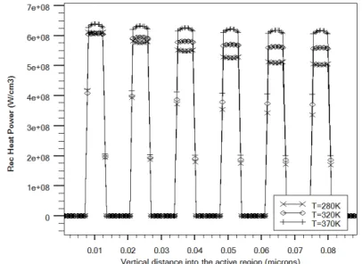
Figure. 15 demonstrates the recombination heat power within a vertical cross-‐section of the active region of BTJ-‐PhC VCSEL structure at 3 V of bias voltage. As can be seen, Increase in the lattice temperature causes the recombination heat power increases which is proportional to gate length because of higher net recombination rate and thermal generation of carriers.
Figure 13: The lattice temperature effect on the total current density within a vertical cross-‐section of the active region.
Figure 14: The lattice temperature effect on the Peltier-‐thomson heat power within a vertical cross-‐section of the active region of BTJ-‐PhC VCSEL.
Figure 15: The lattice temperature effect on the recombination heat power within a vertical cross-‐section of the active region of BTJ-‐PhC VCSEL.
4. CONCLUSION
In this paper, the self-‐heating effects on the characteristics of the 1570 nm InGaAsP BTJ-‐ PhC VCSEL have proposed and investigated. The results show that the output power and current were decreased with increasing lattice temperature due to low thermal conductivity of the BTJ-‐ PhC VCSEL. Also, the effects of lattice temperature increment was analyzed on the various elements of heat sources such as Joule heat, electron–hole recombination heat, Peltier-‐thomson heat within the active region of the BTJ-‐PhC VCSEL. To summarize, lattice temperature increment lead to reduction in the Joule and Peltier-‐thomson heat powers of BTJ-‐PhC VCSEL. In addition, the impact of lattice temperature on the wall-‐plug efficiency and the differential quantum efficiency has also been investigated for BTJ-‐PhC VCSEL structure.
5. REFERENCES
Atlas -‐ Device Simulation Framework. (2018).
http://www.silvaco.com/products/device_simulation/atlas.html
Behrouzinia, S., Khorasani, K., Marjani, S., Sabaghi, M., Aeinehvand, M. E., & Mohammadpour, S. (2016). Experimental Study of Buffer Gas Flow Rate Effect on Output Power of a Copper Vapor Laser. Optics and Photonics Journal, 06(02), 24-‐28.
Deppe, D. G., Li, M., Yang, X., & Bayat, M. (2018). Advanced VCSEL Technology: Self-‐Heating and Intrinsic Modulation Response. IEEE Journal of Quantum Electronics, 54(3), 1-‐9.
Faez, R., Marjani, A., & Marjani, S. (2011). Design and simulation of a high power single mode 1550 nm InGaAsP VCSELs. IEICE Electronics Express, 8(13), 1096-‐1101.
Khafaji, M., Pliva, J., Henker, R., & Ellinger, F. (2018). A 42-‐Gb/s VCSEL Driver Suitable for Burst Mode Operation in 14-‐nm Bulk CMOS. IEEE Photonics Technology Letters, 30(1), 23-‐26.
Majdabadi, A., Marjani, S., & Sabaghi, M. (2014). Threshold Characteristics Enhancement of a Single Mode 1.55 µm InGaAsP Photonic Crystal VCSEL for Optical Communication Systems. Optics
and Photonics Journal, 04(10), 296-‐303.
Marjani, S. (2013). Optimization of an InGaAsP Vertical-‐Cavity Surface-‐Emitting Diode Lasers for High-‐Power Single-‐Mode Operation in 1550 nm Optical-‐Fibre Communication Systems. Asian
Journal of Chemistry, 25(8), 4150–4152.
Marjani, S., Faez, R., & Marjani, H. (2011). Analysis and design of semiconductor laser with silicon carbide polymers (6H-‐SiC and 3C-‐SiC). Asian Journal of Chemistry, 5(7), 1060–1063.
Marjani, S., Faez, R., & Marjani, A. (2011). Design and modeling of a high single mode power long wavelength InGaAsP photonic crystal VCSEL. Australian Journal of Basic and Applied
Sciences, 5(7), 1064–1069.
Marjani, S., Rahnama, M., & Marjani, H. (2011). Numerical optimization of single-‐mode InGaAsP vertical-‐cavity surface-‐emitting lasers. Australian Journal of Basic and Applied Sciences, 5(11), 1207–1211.
Marjani, S., Faez, R., & Marjani, H. (2012). Design and Modeling of a Semiconductor Laser by Employing Silicon Carbide Polymers (6H-‐SiC, 3C-‐SiC and 4H-‐SiC). Asian Journal of Chemistry, 24(5), 2177–2179.
Marjani, S., Faez, R., & Hosseini, S. E. (2013). Analysis of Lattice Temperature Effects on a GaInP/6H-‐SiC Strained Quantum-‐Well Lasers. Asian Journal of Chemistry, 25(9), 4715–4717.
Marjani, S., & Marjani, H. (2012). Effects of hole etching depth in a long wavelength InGaAsP photonic crystal vertical cavity surface emitting laser. Asian Journal of Chemistry, 24(7), 3194– 3196.
Marjani, S., & Marjani, H. (2012). Optimization of a long wavelength vertical-‐cavity surface-‐ emitting lasers by employing photonic crystal. Asian Journal of Chemistry, 24(7), 3174–3176.
Mehta, K., Liu, Y., Wang, J., Jeong, H., Detchprohm, T., Park, Y. J., … Yoder, P. D. (2018). Lateral Current Spreading in III-‐N Ultraviolet Vertical-‐Cavity Surface-‐Emitting Lasers Using Modulation-‐ Doped Short Period Superlattices. IEEE Journal of Quantum Electronics, 54(4), 1-‐7.
Mirzaei, M., Behrouzinia, S., Sabaghi, M., Marjani, S., Khorasani, K., & Sajad, B. (2016). Experimental Optimization of the Output Power of a Copper Vapor Laser Using Air as a Buffer Gas. Optics and Photonics Journal, 06(04), 53-‐59.
Ng, W., Liu, Y., & Hess, K. (2004). Lattice Temperature Model and Temperature Effects in Oxide-‐ Confined VCSEL’s. Journal of Computational Electronics, 3(2), 103-‐116.
Piprek, J. (2003). Semiconductor Optoelectronic Devices: Introduction to Physics and Simulation. UCSB: Academic Press, 9-‐50 and 141-‐147.
Piprek, J., Abraham, P., & Bowers, J. (2000). Self-‐consistent analysis of high-‐temperature effects on strained-‐layer multiquantum-‐well InGaAsP-‐InP lasers. IEEE Journal of Quantum
Electronics, 36(3), 366-‐374.
Piprek, J., Babić, D. I., & Bowers, J. E. (1997). Simulation and analysis of 1.55 μm double-‐fused vertical-‐cavity lasers. Journal of Applied Physics, 81(8), 3382-‐3390.
Piprek, J., White, J., & SpringThorpe, A. (2002). What limits the maximum output power of long-‐ wavelength AlGaInAs/InP laser diodes? IEEE Journal of Quantum Electronics, 38(9), 1253-‐1259.
Qi, C., Shi, X., & Wang, G. (2010). Thermal circuit model of MQW VCSEL laser. 2010 International
Conference on Microwave and Millimeter Wave Technology.
Rissons, A., Mollier, J., Toffano, Z., Destrez, A., & Pez, M. M. (2003). Thermal and optoelectronic model of VCSEL arrays for short-‐range communication. Vertical-‐Cavity Surface-‐Emitting Lasers
VII, 100-‐111.
Streiff, M., Witzig, A., Pfeiffer, M., Royo, P., & Fichtner, W. (2003). A comprehensive VCSEL device simulator. IEEE Journal of Selected Topics in Quantum Electronics, 9(3), 879-‐891.
Szilagyi, L., Khafaji, M., Pliva, J., Henker, R., & Ellinger, F. (2018). 40-‐Gbit/s 850-‐nm VCSEL-‐Based Full-‐CMOS Optical Link With Power-‐Data Rate Adaptivity. IEEE Photonics Technology
Letters, 30(7), 611-‐613.