Felipe Antonio C. Viana
and Valder Steffen, Jr
School of Mechanical Engineering, Federal University of Uberlândia Av. João Naves de Ávila 2121 Campus Santa Mônica P.O. Box 593 38400-902 Uberlândia, MG. Brazil [email protected]Multimodal Vibration Damping
through Piezoelectric Patches and
Optimal Resonant Shunt Circuits
Piezoelectric elements connected to shunt circuits and bonded to a mechanical structure form a dissipation device that can be designed to add damping to the mechanical system. Due to the piezoelectric effect, part of the vibration energy is transformed into electrical energy that can be conveniently dissipated. Therefore, by using appropriate electrical circuits, it is possible to dissipate strain energy and, as a consequence, vibration is suppressed through the added passive damping. From the electrical point of view, the piezoelectric element behaves like a capacitor in series with a controlled voltage source and the shunt circuit, commonly formed by an RL network, is tuned to dissipate the electrical energy, more efficiently in a given frequency band. It is important to know that large inductances are frequently required, leading to the necessity of using synthetic inductors (obtained from operational amplifiers). From the mechanical point of view, the vibration energy can be attenuated in a single mode, or in multiple modes, according to the design of the damping device and the frequency band of interest. This work is devoted to the study of passive damping systems for single modes or multiple modes, based on piezoelectric patches and resonant shunt circuits. The present contribution discusses the modeling of piezoelectric patches coupled to shunt circuits, where the basics of resonant shunt circuits (series and parallel topologies) are presented. Following, the devices used in passive control (piezoelectric patch and synthetic inductors) are analyzed from the electrical and experimental viewpoints. The modeling of multi-degree-of-freedom mechanical systems, including the effects of the passive damping devices is revisited, and, then a design methodology for the multi-modal case is defined. Also, it is briefly reviewed the optimization method used for design purposes, namely the LifeCycle Model. Finally, experimental results are reported, illustrating the success of using the methodology presented in passive damping applications applied to mechanical and mechatronic systems.
Keywords: Multimodal damping, shunted piezoelectric, resonant shunt circuits
Introduction
Applications of smart materials are growing and nowadays they cover from military applications to the industry of consumption. Among other applications, the following can be mentioned:
Vibration damping in sport items represents an important issue for a new generation of ski boards, tennis rackets and golf and baseball bats (Figure 1). The goal here is to reduce vibrations in these sport items, increasing the user's comfort and preventing damage.1
A group composed by Boeing Company, the University of Maryland, the Massachusetts Institute of Technology, the University of California (Los Angeles) and the U.S. Army Research Office support projects for the development and application of smart materials. For example, the Smart Helicopter Rotor can be mentioned (Figure 2), in which fibers of composite materials and piezoelectric devices are used in the blades of the helicopter rotor to attenuate vibrations and noise and also to improve the aerodynamic performance.
Bat
Piezo Element Wiring Harness
Stamped Flats Electronic Shunt Circuit LED Plastic Knob
Wire Slot
Figure 1. Worth Copperhead ACX Adult Baseball Bat, first commercialized in 1998 (adapted from Akhras, 2000).
Paper accepted May, 2006. Technical Editor: José Roberto de França Arruda.
Active plies
Copper/Kapton Electrodes
Piezoceramic Fibers
Polymer Matrix
Figure 2. Smart Helicopter Rotor (http://www.boeing.com/news/releases/, July 2004).
Applications related to vibration control may use either passive or active techniques, as well as a combination of both. Actuators, power supplies and control systems characterize the active techniques. In passive techniques, the power supplies and control systems are suppressed and the shape and physical characteristics of smart materials are explored for vibration reduction.
devices, magnetic devices and passive piezoelectrics. Table 1 shows a comparison of these approaches.
Due to the piezoelectric effect, a portion of the mechanical energy associated with the vibration can be transformed into electric energy and dissipated conveniently, through a shunt circuit that compounds a mechanism of passive damping. Lesieutre (1998) discusses the four commonly used types of shunt circuits: resistive, resonant, capacitive and switched, as shown in Table 2. The abbreviation PZT (lead-zirconate-titanate) refers to the piezoelectric element. This way, CPZT is the inherent capacitance of the piezoelectric patch.
Among the shunt circuits, the resonant one deserves a special attention. Compound by an inductor and a resistor, this circuit
allows the tuning to any desired frequency, which will have the corresponding vibration amplitudes attenuated. In addition, improvements in the topology of the circuit make possible the simultaneous reduction of more than one vibration mode. From the mechanical point of view, the system as a whole (PZT and resonant shunt circuit) is similar to the dynamic vibration absorber.
A detailed description of the use of shunt circuit and piezoelectric devices is seen in the pioneer work of Hagood and von Flotow (1991). In that work, the expression for the mechanical impedance introduced by the piezoelectric element connected to any type of shunt circuit coupled to mechanical systems is obtained. Two study cases are presented, showing experiments with shunt circuits, both resistive and series resonant types.
Table 1. Primary passive damping mechanisms and correlated information (adapted from Johnson, 1995). Type of damping mechanism
Viscoelastic materials Viscous devices Magnetic devices Passive piezoelectrics
Type of treatment All Struts and DVAs* Struts and DVAs Strut dampers
Temperature sensitivity High Moderate Low Low
Temperature range Moderate Moderate Wide Wide
Loss factor Moderate High Low Low
Frequency range Wide Moderate Moderate Moderate
Weight Low Moderate High Moderate
(*)DVA: Dynamic Vibration Absorber.
Table 2. Shunt circuits (adapted from Lesiutre, 1998).
Resistive Resonant Capacitive Switched
+
-R CPZT P
Z
T +
-R
L CPZT P
Z
T +
-CPZT P Z T
C
+
-CPZT P Z
T ZSHUNT
This circuit results a behavior that is similar to viscoelastically-damped systems.
This circuit behaves similarly to the classical dynamic vibration absorber.
This circuit changes the stiffness of the piezoelectric element.
The most important feature of this circuit is to adjust the behavior of the circuit in response to any change in the system.
A series of papers have been reported about the present topic. Wu (1996) makes considerations about the behavior of the resonant shunt circuit in the parallel topology. Steffen and Inman (1999) use control techniques and optimization strategies in the design of both active and passive vibration reduction devices, using piezoelectric materials. Steffen et al. (2000) examine the use of passive techniques for vibration reduction combining dynamic vibration absorbers (DVAs) and piezoelectric patches coupled to resonant shunt circuits. In that work, natural optimization techniques were used in the design of the damping system. Park and Inman (2003) discuss the non-idealities of the synthetic inductor used in the shunt circuits and propose an improvement by adding capacitors in parallel to the piezo, aiming at reducing the values required for the inductance.
This work is devoted to the study of passive damping systems for single modes or multiple modes. As compared to previous contributions, this paper presents a complete study concerning resonant shunted piezoelectric, including the analytical and experimental aspects together with the synthetic inductor design. Besides, the study devoted to the multimode case represents a more realistic approach. Previous works considered the multimode case a simple extension of the single mode case. Also, the use of optimization techniques is considered a valuable contribution because no closed solution can be derived for the multimode case. The optimization results were validated experimentally. The present
contribution is organized as follows: first, the modeling of piezoelectric patches coupled to shunt circuits, where the basics of resonant shunt circuits (series and parallel) are presented together with a literature review about this topic; following, the devices used in passive control (piezoelectric patch and synthetic inductors – Riordan and Antoniou types) are analyzed from both the electrical and experimental viewpoints; then the modeling of multi-degree-of-freedom mechanical systems, including the effects of the passive damping mechanism is presented; in the sequence, a new design methodology for the multi-modal case is proposed. Also, the optimization method used for design purposes, namely the LifeCycle Model, is briefly reviewed. Finally, experimental results are reported, illustrating the success of using the methodology presented as applied to passive damping applications of mechanical and mechatronic structures.
Nomenclature
A= the matrix of surfaces, perpendicular to the electric field
Ai and Aj = the transversal section areas according to the vectors i and j [m2]
B = the diagonal matrix of the lengths of the piezoelectric
Bi and Bj = the initial patch lengths according to vectors i
and j [m] T
PZT
C = the inherent capacitance of the piezoelectric patch taken at constant stress (free)
D = the vector of electrical displacement [C/m2]
E = vector of electric field [V/m] I = the electric current
K = the stiffness of the mechanical system E
Kjjis the stiffness of the piezoelectric patch taken in open circuit
L = the inductance
PZT = piezoelectric patch
R= the resistance
S = the vector of material engineering strains
(non-dimensional)
Sj = the strain (non-dimensional)
T = vector of material stresses [N/m2] Tj = the stress [N/m2]
V = the electric voltage Y = the electric admittance
( )
ZSHUNTi s = the electrical impedance of the shunt circuit [Ω]
( )
SHUNT
Zjj s = the mechanical impedance of the passive damping
device with the shunt circuit shunt
d = the piezoelectric material constant relating strain to voltage [m/V]
dij = the piezoelectric material constant relating voltage in ith
direction to strain in the jth direction
i and j = coordinate axes that indicate the direction for
electrical and mechanical vectors
k = electromechanical coupling coefficient
r
k = the modal stiffness related to the mode r
r
m = the modal mass related to the mode r
s = the matrix of compliance for the material [m2/N] s= the Laplace variable
Greek Symbols
ε
= the matrix of dielectric constants for the material [C2/(N.m2)]
δ= the non-dimensional tuning ratio
0
ω = the electrical resonance frequency [rad/s]
n
ω = the resonance frequency of the mechanical system [rad/s]
ξ = the damping factor
γ = the non-dimensional frequency Subscripts
PZT relative to the piezoelectric patch Superscripts
E value taken at constant field (short circuit) ELECT relative to an electrical parameter
D value taken at constant electrical displacement (open
circuit)
MEC relative to a mechanical parameter RSP pertaining to resonant circuit shunting S value taken at constant strain (clamped) OPTM relative to the optimal condition
PARALLEL relative to the parallel circuit topology
SERIES relative to the series circuit topology SHUNT relative to the shunt circuit
T value taken at constant stress (free) t transpose of the vector or matrix
Modeling Piezoelectric Patches coupled to Shunt Circuits
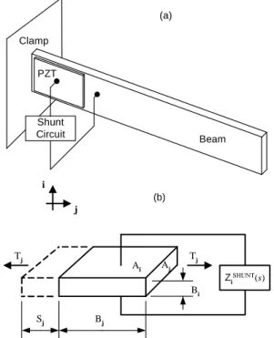
Figure 3 illustrates the case in which a piezoelectric patch is coupled to a shunt circuit and bonded to a flexible structure. Figure 3-(a) shows the complete system and Figure 3-(b) depicts the simplified model for the passive damping device.
Shunt Circuit Clamp
Beam PZT
(a)
ZiSHUNT(s)
Bj
Bi
Sj
Tj Tj
Ai Aj
i
j
(b)
Figure 3. Model for a piezoelectric patch bounded to a shunt circuit.
where:
•PZT is the piezoelectric patch,
• ZiSHUNT( )s is the electrical impedance of the shunt circuit [Ω], • i and j give the coordinate axes that indicate the direction for
electrical and mechanical vectors, • Tj is the stress [N/m2],
• Ai and Aj are the transversal section areas according to the vectors i and j [m2],
• Bi and Bj are the initial patch lengths according to vectors i and j [m],
• Sj is the strain (non-dimensional), and •
s
is the Laplace variable.As in Hagood and von Flotow (1991), the general expression that describes the behavior of piezoelectric materials, such as the one shown in Figure 3, is written as:
T
t E
=
D ε d E
S d s T (1)
where:
• E is vector of electric field [V/m],
• S is the vector of material engineering strains (non-dimensional), • T is vector of material stresses [N/m2],
• ε
is the matrix of dielectric constants for the material [C2/(N.m2)], • s is the matrix of compliance for the material [m2/N], and • d is the piezoelectric material constant relating strain to voltage
[m/V].
Hagood and von Flotow (1991) also shows how to use Eq. (1) together with the basic equations of voltage and current from the electricity in order to obtain the following expression:
1 ( )
;
ELECT
t E
ELECT D SHUNT
PZT s s − = = +
I Y Ad V
S d B s T
Y Y Y
(2)
where:
• Vis the electric voltage, • I is the electric current,
• B is the diagonal matrix of the lengths of the piezoelectric patch, • A is the matrix of surfaces, perpendicular to the electric field, • Y is the electric admittance, and
• D T
PZT=sCPZT
Y .
At this time, it is important to define the piezoelectric constant known as electromechanical coupling coefficient, k . Hagood and von Flotow (1991) define this constant as being the relationship between the peak energy stored in the capacitor and the peak energy stored in the deformation of the material taking into account open electrodes for the piezoelectric patch. Physically, the square of this coefficient, k , represents the percentage of energy of mechanical 2
deformation that can be turned into electric energy and vice-versa. Mathematically, the electromechanical coupling coefficient is defined as: E T d k s ε = ij ij jj i (3)
where dij is the piezoelectric material constant relating voltage in the ith direction to strain in the jth direction.
To close the modeling, Hagood and von Flotow (1991) show the mechanical impedance, in the non-dimensional form, for the piezoelectric patch with a shunt circuit as defined by the equation:
2
2
( ) 1
( )
( ) 1 ( )
SHUNT MEC
D ELECT
Z s k
Z s
Z s k Z s
−
= =
−
jj ij
jj
jj ij i
(4)
where ZjjSHUNT( )s is the mechanical impedance of the passive
damping piezo device with the shunt circuit.
Finally, Hagood and von Flotow (1991) show that the frequency response function (FRF) that relates the acceleration and the external force of a resonant shunted piezoelectric in the Laplace domain is:
( )
2 2 ( ) H MEC r r s sk sZ s s m
=
+ jj +
(5)
This equation is valid for a single mode system, thus m and r k r
are the modal mass and modal stiffness related to the mode r.
Resonant Shunted Piezoelectrics - RSPs
According to what has been seen up to now, the piezoelectric patches can be modeled as a capacitor in series with a controlled voltage source. Therefore, in order to obtain a resonant shunt circuit, the circuit shown in Figure 3 can be compound of an inductor and a resistor. The RL shunt circuit forms an RLC resonant network with the piezoelectric patch. This approach allows the dissipation of the energy associated with a given vibration mode. In this case, the strain energy (associated with the vibration) is converted into electric energy and dissipated in the form of heat, through the Joule effect. From the mechanical point of view, damping is introduced by appropriate tuning the resonance frequency of the RLC network to a given frequency related to one of the vibration modes of the mechanical structure.
Series Resonant Shunt Circuit
The resonant shunt circuit in series, as shown in Figure 4, was proposed by Hagood and von Flotow (1991). The same scheme can be found in Lesieutre (1998), Steffen and Inman (1999), Caruso (2001), Fleming et al. (2002), Fleming et al. (2003) and Park and Inman (2003).
Bj
Bi
Sj
Tj Tj
Ai Aj i j R L +
-CPZT P
Z T
R
L
Figure 4. The series resonant shunt circuit.
An analysis of this circuit leads to the following relations:
2 2 1 ( ) ( ) 1 ; SHUNT T T
ELECT PZT PZT
T T
PZT PZT
Y s
Ls R
LC s RC s
Z s
LC s RC s
= + + = + + i i (6) where:
• T
PZT
C is the inherent capacitance of the piezoelectric patch taken at constant stress (free).
Or, using Eq. (4), the non-dimensional impedance can be written as:
2
2 1 ( ) 1
1
SERIES RSP
S S
PZT PZT
Z s k
LC s RC s
= − + + ij jj (7)
Equation (7) can be rewritten as:
2 2
2 2 2
( ) 1
SERIES RSP
Z γ k δ
γ δ ξγ δ
= − + + ij jj (8) where: • 0 n ω
δ= ω is the non-dimensional tuning ratio,
• 0 1 S
PZT LC
ω = is the electrical resonance frequency,
• ω =n KM is the resonance frequency of the mechanical
system,
• S E
PZT n RC
ξ= ω is the damping factor,
•
(
)
E E n K K Mω = + jj
is the resonance frequency of the mechanical system, corresponding to the open circuit case, • K is the stiffness of the mechanical system,
• E E A K s L = j jj jj j
is the stiffness of the piezoelectric patch
corresponding to the open circuit case, and
• E
n s γ
ω
= is the non-dimensional frequency.
Hagood and von Flotow (1991) point out that the parameters δ and ξ are similar to those found for the DVA. Consequently, the series resonant shunt circuit can be designed by considering these similarities.
Figure 5 illustrates the two above-mentioned configurations for vibration reduction purposes. Figure 5-(a) shows a system containing a DVA; and Figure 5-(b) depicts a system containing an RSP.
M MDVA
K
KDVA CDVA
f(t) = Fsin(ωt)
x(t) Primary System Dynamic vibration absorver (DVA) M K
f(t) = Fsin(ωt)
x(t) Primary System RSP
(a)
(b)
Figure 5. Comparison between systems with a DVA (a) and an RSP (b).
The generalized electromechanical coupling coefficient is defined as: 2 2 2 2 2 1 1 E E
K k k
K K
K K k k
= =
+ − −
jj ij ij
ij
jj ij ij
(9)
where K is the ratio between the piezoelectric short circuit modal stiffness and the total system modal stiffness.
Now, it is possible to compare the frequency response functions for the DVA and the RSP, as calculated for the primary mass for both cases:
(
)
( )(
) (
)
2 2 2
2 2 2 2 2 2 2
( ) 1 SERIES P RSP M H K
δ γ δ ξγ
γ
γ δ γ δ ξγ γ δ ξγ
+ +
=
+ + + + ij +
(10)
(
)
( )(
) (
)
2 2 2
2 2 2 2 2 2 2 3
( ) 1
P DVA M
H γ δ γ δ ξγ
γ δ γ δ ξγ µ δ γ δ ξγ
+ +
=
+ + + + + (11)
Equations (10) and (11) highlight the similarities between the DVA and the RSP. It can be seen that the generalized electromechanical coupling coefficient, Kij2, for the system with RSP series is similar to the relationship between the mass of the DVA and the mass of the primary structure, µ, for the system with DVA. However, notice that the DVA operates by absorbing the kinetic energy associated to the vibration of the primary structure. The RSP, in a general way, dissipates a portion of the strain energy that is converted into electric energy. As a consequence, the optimal locations for each type of damping system are different: the DVA should be connected to a point of maximum displacement and the piezoelectric patch of an RSP should be bonded to a region of maximum deformation.
Similarly to the system with a DVA, the design of the optimal RSP series is obtained from the optimal tuning ratio, δ, and the optimal damping factor, ξ, for the system. Therefore, these expressions are as below:
(
)
2 2 1 2 1 SERIES SERIES RSP OPTM RSP OPTM K K K δ ξ = + = + ij ij ij (12)Figure 6 illustrates the transfer function of the system with an RSP series, adopting Kij2=0.05, RSPSERIES
OPTM
δ δ= , and considering the
non-dimensional frequency
n
g=ωω , for different values of ξ.
Figure 6. Transfer function of the primary mass for systems with an RSP series.
Finally, once the optimal parameters δ and ξ for the RSP series are obtained, it is possible to determine the optimal values for the inductor and resistor of the shunt circuit, from the following equations:
(
)
( )
( )
2 2 2 2
0
2
1 1 1
1 2 1 SERIES SERIES SERIES SERIES RSP
OPTM S S RSP S
PZT PZT n OPTM PZT n
RSP
ij
RSP OPTM
OPTM S S
PZT n PZT n
L
C C C K
K R
C C K
ω ω δ ω
ξ ω ω = = = + = = + ij ij (13)
Parallel Resonant Shunt Circuit
The parallel resonant shunt circuit (see Figure 7) was first proposed by Wu (1996), aiming at overcoming implementation difficulties of the series circuit. The practical aspects regarding the two circuit topologies will be discussed in the later sections.
Bj
Bi
Sj
Tj Tj
Ai Aj i
j
R L
+
-CPZT P
Z T
R L
Figure 7. The parallel resonant shunt circuit.
As in the series circuit, the analysis of the electrical circuit leads to the following equations:
2 2 1 1 ( ) ( ) SHUNT T ELECT PZT T PZT Y s Ls R LRC s Z s
RLC s Ls R
= + = + + i i (14) And, consequently: 2 2 2 2 2 2 2
( ) 1
( ) 1
PARALLEL PARALLEL RSP S PZT RSP Ls R
Z s k
RLC s Ls R
Z s k γ ξδ
ξγ γ ξδ
+ = − + + + = − + + ij jj ij jj (15)
Using Eq. (15) and the proper modeling of the single DOF system, it is possible to obtain the transfer function as:
(
)
(
)( )
2 2
2 2 2 2 2
( ) 1 PARALLEL P RSP M H K δ ξ γ ξ γ γ
δ ξ γ ξ γ γ γ ξ
+ +
=
+ + + + ij
(16)
Wu (1996) presents details for obtaining the optimal parameters of the circuit. Similarly to Hagood and von Flotow (1991), he also makes use of the transfer function to draw his conclusions. This way, the expressions are:
2 1 2 1 2 PARALLEL PARALLEL RSP OPTM RSP OPTM K K δ ξ = + = ij ij (17) And consequently: 2 2 1 1 2 1 2 PARALLEL PARALLEL RSP OPTM S PZT n RSP OPTM S PZT n L K C R K C ω ω = − = ij ij (18)
Figure 8 shows the transfer functions of the system with an RSP parallel, adopting Kij2=0.05, SERIES
RSP OPTM
δ δ= , and considering the
non-dimensional frequency
n
Figure 8. Transfer function of the primary mass for systems with an RSP parallel.
Electric Analysis of the Shunted Piezoelectric Components
The following sections show the analysis of the piezoelectric patch and the synthetic inductors from the electrical viewpoint. For the piezoelectric patch, the associated impedance and its behavior are verified when bonded to a vibratory structure. Two basic types of synthetic inductors are presented.
The Piezoelectric Patch
As an example, the manufacturer (Mide Technology Corporation) provides the information presented in Tab. 3 about the ACX QP15N piezoelectric patch.
Table 3. ACX QP15N specifications.
Size [mm] Weight[g] Number of
elements
50.8 x 25.4 x 0.254 2.268 1 piezoelectric patch
Piezoelectric patch
size [mm] Capacitance [nF]
Operation range [V]
45.974 x 20.574 x
0.127 100 ± 100
However, for the system compound by an ACX QP15N bonded to a flexible beam as shown in Figure 9, by using an impedance analyzer (Hewlett Packard HP4194A), a variation of the impedance with respect to the frequency is found, as shown by Figure 10.
Figure 9. ACX QP15N + Beam System.
Figure 10 shows also that impedance is not purely reactive. The real part of the impedance, Figure 10-(a), introduces a resistive element. Besides, the imaginary part of the impedance, Figure 10-(b), confirms the capacitive element. From the phase curve, Figure 10 -(d), the predominance of the capacitive component is verified, since
the values obtained are close to –90º. The inherent impedance of the piezoelectric patch can be viewed as a resistor, Figure 10-(e), which is in series with a capacitor, Figure 10-(f).
Figure 10. Impedance for the ACX QP15N + Beam system.
To validate the above-presented model, the ACX QP15N + beam system is tested using the setup shown in Figure 11.
Flexible Beam
Piezoelectric Device RLOAD
Shaker
Figure 11. Experimental setup for the verification of the electrical characteristics of the ACX QP15N + Beam + RLOAD system.
A shaker excites the system according to a predefined frequency and amplitude. Therefore, according to the modeling of the piezoelectric device, the controlled voltage source (internal to the patch) also produces voltage. Electrically, the set constituted by the piezoelectric patch and load resistance forms a circuit characterized by a voltage source, a capacitor, a resistor and a load resistance, as shown in Figure 12.
CPZT
RPZT
RLOAD
VIN
VOUT
PZT I
Figure 12. Resultant electric circuit from the ACX QP15N + Beam + RLOAD system.
This way, the current and the electric power on RLOAD can be calculated by using the Ohm’s law:
(
)
2( ) ( )
( )
( )
IN OUT
TOTAL LOAD
RMS OUT RMS RMS
LOAD OUT
LOAD
V V
I
Z R
V
P V I
R
ω ω
ω
ω
= =
= =
Experimentally, the voltage VIN( )ω can be obtained through an oscilloscope, by keeping the terminals of the piezoelectric element in open circuit, as illustrated in Figure 13. VIN( )ω depends on the magnitude of the excitation provided by the shaker. As the excitation remains the same , VIN( )ω is not altered.
CPZT
RPZT
VIN
PZT Oscilloscope
Figure 13. Setup for the experimental obtaining of VIN(ωωωω)))).
Consequently, by varying the load resistance and measuring the voltage in the load resistance, the curves corresponding to
x
OUT LOAD
V R , I x RLOAD and PLOAD x RLOADcan be generated. Figure 14 illustrates the comparison of the experimental data with those obtained from the analytical model of the proposed electric circuit.
Figure 14. Experimental versus analytical data for the ACX QP15N + Beam + RLOAD system.
The Resonant Shunt Circuit and the Synthetic Inductor
Equations (13) and (18) show that the values of the inductance are inversely proportional with respect to the angular frequency. In the real cases, the associated frequencies are relatively low. As a consequence, the resonant shunt circuits require large values for the inductance. These values would typically attain hundreds of henries. The weight and the volume of such inductors would make unfeasible the use of this technique. To overcome this limitation, synthetic inductors are obtained by using operational amplifiers, as in previous works (Riordan, 1967; Antoniou, 1969; Stephenson, 1985; Schaumann et al., 1990; Massara et al., 2000 and Park and Inman, 2003). Even assuming different configurations, these circuits are known as synthetic inductors or gyrators. In the present contribution, two types of synthetic inductors were explored, namely the one proposed by Antoniou (1969), and the other one based on Riordan (1967). For the sake of simplicity, they are called Antoniou synthetic inductor and Riordan synthetic inductor, respectively.
Antoniou Synthetic Inductor
Figure 15 shows the synthetic inductor circuit as proposed by Antoniou (1969).
OA1
OA2
Z1 Z2 Z3 Z4
Z5
ZIN
V1 I1 V2 I2 V3 I3 V4 I4 V5
Figure 15. Circuit for the Antoniou synthetic inductor.
The input impedance is given by equation (20):
1 3 5
2 4
IN Z Z Z Z
Z Z
= (20)
From the previous equation, a synthetic inductor is obtained by using the following relations: 4
4
j
Z =− ωC , Z1=R1, Z2=R2,
3 3
Z =R and Z5=R5. The equivalent circuit impedance ZIN is the same as an inductor (L ), as shown below: eq
1 3 4 5
2 ;
IN eq
eq
Z j L
R R C R L
R ω =
=
(21)
Riordan Synthetic Inductor
Z1
Z2
Z3
Z4
Z5
OA2
OA1
V1
V2
V3
ZIN
Figure 16. Circuit for the Riordan synthetic inductor.
In despite of presenting a different topology, the equations for the input impedance are the same as those of the Antoniou synthetic inductor.
Practical Aspects about the Synthetic Inductors
In order to test the performance of synthetic inductors at low electrical frequencies (as typically found in most mechanical systems), experiments simulating the resonant shunt circuit were performed. An RLC series filter was configured in this experiment by using the synthetic inductor together with a resistor R , a 0
capacitor CPZT and a signal generator (Brüel & Kjær Sine/Noise Generator Type 1049). The filter is described by Eq. (22), which relates the voltage in R and the voltage in the generator. A signal 0
analyzer (Spectral Dynamics SD380) was used to perform the frequency analysis of the circuit. The setup of the experiment is shown in Figure 17.
1 ( )
1 1
1
LOAD
PZT H
j L
R C
ω
ω ω
=
+ −
(22)
SD380 Analyser PC
B&K - Sine/Noise Generator
CPZT R0
Synthetic Inductor VIN
VOUT
Figure 17. Experimental setup to test the synthetic inductors.
The signal generator introduces in the circuit a white noise of bandwidth 2Hz to 2kHz, with 1.25V of RMS value. The signals were acquired simultaneously in a sample of T=1.6s, with intervals of
dt=0.78125ms. Then the maximum frequency analyzed is fmax=500Hz and the frequency resolution is df=0.625Hz. The
transfer function was estimated by using 50 samples.
The capacitors C and 4 CPZT and the resistor R were fixed to 0 108.5nF, 110.1nF and 9.98kΩ, respectively. Table 4 shows the values used for the remaining components along the experiments. In this case, the inductance is calculated according to the equation:
(
)
21 2
eq
elet PZT L
f C
π
= (23)
Table 4. Experimental values for R1, R2, R3 and R5 and the calculated one for Leq.
Experiment R [k1 Ω] R [k2 Ω] R [k3 Ω] R [k5 Ω] L [H] eq
#1 2.18 2.17 97.7 2.16 23.00
#2 5.51 5.52 38.6 5.51 23.03
#3 14.78 14.68 14.35 14.67 22.0
#4 46.2 46.2 4.61 46.0 23.01
#5 99.9 99.3 2.13 99.1 23.04
#6 219 220 0.964 221 23.01
#7 330 329 0.643 329 23.02
Figure 18 and Figure 19 present the graphics of the amplitude, phase and coherence of the transfer function for the two types of synthetic inductors. A comparison between the two types of synthetic inductors does not allow any straightforward conclusion about the superiority of one with respect to the other. However, by taking into account the graphics of the module and phase, it is possible to notice good repeatability for the tests, since the resonance frequency remains approximately the same for all the experiments. The graphics of the coherence indicate that along the experiments the values of the coherence become worse, probably due to the values of the resistors. Finally, it is also possible to notice that the electric network available contaminates the experiments in 60Hz (used in Brazil) and in some other harmonics in all the experiments.
Figure 19. Amplitude, phase and coherence of the transfer function for Riordan synthetic inductor.
Figure 18 and Figure 19 also show a discrepancy between the experimental results and the analytical model adopted for the RLC circuit, as described by Eq.(22). For example, in all cases the gains are not unitary in the resonant frequency. It can be concluded that the non-idealities of the synthetic inductor generate one or more parasite resistances associated with the equivalent inductor. Park et al (2003) discussed about an experiment that evaluates the impedance of the synthetic inductor. By using an impedance analyzer, it was shown the existence of a frequency dependent inherent resistance in the synthetic inductor.
In this work, it is desired to obtain an equivalent model for the synthetic inductor. To achieve this aim, four different configurations were tested as candidates for the equivalent circuit used in the experiments, as shown in Figure 20.
CPZT
PZT R0
synthetic inductor
RS
Leq
(a)
CPZT
PZT R0
synthetic inductor
RP Leq
(b)
CPZT
PZT R0
synthetic inductor
RS
Leq RP
(c)
CPZT
PZT R0
synthetic inductor
RS
Leq RP
(d)
Figure 20. Candidate configurations to the synthetic inductor equivalent circuit (a) a resistor RS in series with an inductor Leq , (b) a resistor RP in parallel with an inductor Leq ,(c) a resistor RP in parallel with an inductor Leq and a resistor RS in series with this branch and (d) a resistor RS in series with an inductor L and a resistor R in parallel with this branch.
Experiment #4 for the Riordan synthetic inductor was arbitrarily chosen to check which model better describes the behavior of the real circuit. From a curve fitting procedure, it was possible to obtain the values of R and S R , as presented in Table 5 and Figure 21. P
Table 5. Values of RS and Rp.
Circuit
Figure 20-(a)
Circuit
Figure 20-(b)
Circuit
Figure 20-(c)
Circuit
Figure 20-(d)
S R
[kΩ]
P R
[kΩ]
S R
[kΩ]
P R
[kΩ]
S R
[kΩ]
P R
[kΩ] 4.969 72.495 3.067 140.591 3.506 5.398 x 10¹¹
Figure 21. Amplitude and phase of the experimental and analytical transfer functions.
By analyzing Table 5 and Figure 21, it can be concluded that the best representation of the real electrical circuit is given by the circuit (a), for which the synthetic inductor is characterized as a resistor RS in series with an equivalent inductor L , as described by Eq. (22). Circuit (d) presents very similar results, however, the value of the resistor R is extremely high, suggesting that P R tends to infinite P
(open circuit). This characteristic automatically leads to the choice of circuit (a). In this work, the inherent resistance of the synthetic inductor is called RPARASITE.
values of R and 0 C were fixed to 9.86k0 Ω and 111.5nF, respectively, and a number of different values for the resonance frequency of the circuit, f , was predefined. Consequently, the 0 value of the inductor varies, leading to the variation of RPARASITE. For both considered inductors the values of R , 0 R , 1 R , 2 R , 5 C 0
and C were fixed to 9.86k4 Ω, 46.2kΩ, 46.2kΩ, 46.0kΩ, 111.5nF, and 112.6nF, respectively.
The results can be seen in Table 6 and Figure 22.
Table 6. Experimental value for f0, Leq and RPARASITE. Antoniou Synthetic Inductor
Experiment f [Hz] 0 L [H] RPARASITE[kΩ]
#1 396.25 1.3573 0.9553
#2 301.25 2.3175 1.1314
#3 198.75 5.3116 1.7849
#4 100.00 20.6205 4.0478
#5 49.375 81.4147 10.9426
#6 22.50 368.4433 39.4855
Riordan Synthetic Inductor
Experiment f [Hz] 0 L [H] RPARASITE[kΩ]
#1 401.875 1.4682 1.0776
#2 297.500 2.5302 1.2170
#3 200.000 5.3308 1.7967
#4 99.375 20.5834 4.2154
#5 48.750 81.5618 11.1978
#6 23.125 368.1111 37.6879
Figure 22. RPARASITE versus L for the synthetic inductors.
Both for the Antoniou and for the Riordan synthetic inductors, it is easy to notice that the value of the parasite resistance increases when the inductance values also increase. This behavior is quite linear along the analyzed range. This means that, by taking into account a pre-defined value for the capacitance, the RLC filters exhibit better performance when designed to operate at larger electrical resonance frequencies. This fact has a direct consequence in shunted piezoelectric applications, since the frequencies of interest in these cases are rather low from the electrical point of view.
Multiple Degree-of-Freedom (MDOF) Systems
Real systems are continuous and non-homogeneous, which means that an infinite number of degrees of freedom should be considered to represent them, accordingly. Therefore, the analysis of this type of systems is only possible through analytic (exact) models. Unfortunately, the solution of these models is not easily obtained. Thus, it is necessary to use approximate techniques that describe the behavior of the system by using a finite number of degrees of freedom (Maia and Silva, 1997). To exemplify, consider the undamped N DOF system shown in Figure 23.
mN
m1 m2
k1 k2 k3 kN kN+1
…
x1 x2 xN
f1 f2 fN
Figure 23. Discrete model for an N degrees of freedom system.
The equation of motion can be written in the matrix notation as:
2 ω
− =
K M x f (24)
By taking f=0, it is possible to obtain the modal model for the free system, which is commonly expressed by the following pair of NxN matrices:
{ } { }
{ }
2 1
2
2 2
2
1 2
0 0
0 0
0 0
r
N
N
ω ω ω
ω
ψ ψ ψ
=
=
ψ
⋯ ⋯
⋮ ⋮ ⋱ ⋮
⋯ ⋯
(25)
The eigenvalues ω12,ω22,...,ωN2 represent the natural
frequencies of the undamped system. The eigenvector matrix ψ
(also known as the modal matrix of the system), is compound by the modal shapes given by
{ }
ψr (r = 1, 2, ..., N).In order to find the FRF of the system, it is necessary to perform the following matrix transformations:
[ ] [ ][ ] [
]
[ ] [ ][ ] [
]
`
` `
`
t
r t
r m
k = =
ψ
M ψ
ψ
K ψ
(26)
The FRF that relates the acceleration obtained at the position i
when an external force is applied at the position k is given by the
following equation:
2 2 1
( ) i k
ik H
N
r r
r r r
s s
k s m ψ ψ
=
=
+
∑
(27)For more details about MDOF systems refer to Maia and Silva (1997).
Modeling of Shunted Piezoelectrics for MDOF Systems
As previously shown in Viana (2005), it is possible to note the similarity between Eq. (5), which describes the system of 1 DOF containing the shunted piezoelectric device and Eq.(27), which describes a MDOF system. It can be observed that Eq. (27) takes into account the influence of the N modes in the system response.
This way, by considering the analyses above, the effect of the piezoelectric patches and their shunt circuits can be easily introduced in the MDOF system. This can be achieved by adding the term ZMECr( )s
jj in the denominator of Eq. (27). Mathematically:
( )
2
2 1
( ) i k
ik H
r N
r r
MEC
r r r
s s
k sZ s m
ψ ψ ω
=
=
+ +
∑
jj
(28)
It is worth mentioning that m and r k in Eq. (28) include the r
influence of the PZT (Pereira, 2003).
As an example, consider the case as depicted in Figure 24. This figure illustrates an undamped flexible beam (a) containing two piezoelectric passive damping devices (b). A PZT and its corresponding shunt circuit characterize each passive device. Damping in this case is designed to reduce the vibration amplitudes of two pre-defined modes, simultaneously.
(a)
Clamp
Beam
(b)
Clamp
Beam PZT 01
Shunt Circuit 01
Shunt Circuit 02
PZT 02
Figure 24. Beam (a) without and (b) with piezoelectric shunt devices.
Figure 25 shows the FRF obtained numerically. The circuits were designed to reduce the vibration amplitudes of the second and third modes, simultaneously.
Figure 25. FRF for systems with and without passive damping.
Optimal Design Strategy for Multimodal Shunted Piezoelectrics
Equation (28) shows that a modification introduced in any mode influences the FRF in the whole frequency band. This means that the effect of a resonant shunt circuit, tuned for a specific mode, does not influence only that single frequency, but the whole frequency band. Therefore, considering the design for multimodal passive vibration suppression systems, the circuits cannot be designed separately, using closed solutions, as for the single mode case. Thus, the most effective strategy should consider the influence of each mode and the band of interest. In this work, the design of the resonant shunt circuits is treated as an optimization problem, as presented in Steffen and Inman (1999) and Rade and Steffen (2000). For illustration, consider the situation shown in Figure 24-(b) and described by Eq. (28). The response, Hik( )s , must be minimized over predefined frequency bands as chosen by the user. For example, in the case illustrated by Figure 24 and Figure 25, the second and third modes were taken as target modes for attenuation purposes. Consequently, in the most general case, the system may have a group of N piezoelectric patches and their shunt circuits, each one tuned up for a different mode. Under these circumstances, the optimal design of shunt circuits consists of determining the value of each one of the N inductors and N resistors to be used in the shunt circuits.
Then, the optimization problem is defined as the minimization of the objective function given by:
{ } { }
1
( , ) ( )
p
ik m m
J L R H s
=
=
∑
(29)subject to:
,
1, 2,..., ,
upper lower
i i i
upper lower
i i i
L L L
i N
R R R
< <
=
< < (30)
where:
• p: is the number of values ofHik( )s ; these values are
piezoelectric shunt systems as shown in the previous section,
• Hik( )s : is the frequency response function,
•sm : represents the Laplace variable within the frequency band of interest;
• Li and Ri: are the inductors and resistors to be used in the damping of the ith mode, respectively, and
• N: is the number of shunt circuits to be used.
The optimization task that defines the design of the shunt circuits is an example of direct problem. In spite of this, the use of classical optimization methods fails in many cases, due to local minima found in the design space. For this reason, in the present work, a natural optimization method was used, namely the LifeCycle Model, to be briefly reviewed in the following sub-section.
LifeCycle Model – an Overview
LifeCycle Model (Krink and Løvberg, 2002) is inserted in the natural optimization context, in which Genetic Algorithms (GA) and Particle Swarm Optimization (PSO) also belong. In biology, the term refers to the passage through the phases during the life of an individual. As life phases, can be cited the sexual maturity and the mating seasons, for example. As it happens in nature, the ability of an individual to actively change its own phase or stage in response to its success in the environment is the main inspiration for LifeCycle. In fact, the idea behind LifeCycle is to use the transitions to deal with the mechanism of self-adaptation to the optimization problem. The fitness offers a criterion used by each individual to shift to another life stage. To close the definition, LifeCycle stages must be presented. In the present work, two heuristics are used as stages, namely the GA and the PSO. Other versions of the LifeCycle can be proposed by considering other heuristics and a mix of them, as shown in Krink and Løvberg (2002).
Since the algorithm is composed by various heuristics, it is necessary to set the parameters of every heuristic used in the LifeCycle model. Nevertheless, there is a parameter inherent to the LifeCycle model, namely the number of iterations that represents a stage of the LifeCycle, called as stage interval. At the end of each stage interval, the less well-succeeded individuals must change their stage in order to improve their fitness. This means that the optimization approach does not follow a rigid scheme as proposed in Assis and Steffen (2003), in which various techniques are used sequentially in a cascade-type of structure. In other words, it is the mechanism of self-adaptation to the optimization problem that counts.
It is important to notice that the algorithm can run in a parallel scheme, since the original population is divided in a subpopulation of PSO particles and another one of GA individuals. During the optimization procedure the agents of each subpopulation commute to the other in a way to improve its own fitness.
Details about GA are provided by Michalewicz (1994) and Haupt and Haupt (1998), while PSO is comprehensively presented by Kennedy and Eberhart (1995) and Venter and Sobieski (2002).
The outline of a basic LifeCycle algorithm is presented below: 1. Initialize the algorithm parameters for the PSO and GA. 2. Evaluate the fitness for all particles (PSO) and individuals
(GA).If there is no recent improvement, switch the LifeCycle stage (change from GA to PSO or vice-versa).
3. For all PSO particles, run the PSO algorithm. 4. For all GA individuals, run the GA algorithm.
5. Go to step 2 and repeat until the stop criteria are achieved.
For more detailed information about LifeCycle Model the reader should refer to (Rojas et al., 2004).
Experimental Results
Using a mechanical system composed by a flexible beam, two piezoelectric patches and their respective shunt circuits, it was possible to perform the experimental verification of the design methodology presented above. Figure 26 shows details of the experimental setup. Figure 26-(a) gives the configuration used for single mode vibration suppression, in which a single piezoelectric patch and shunt circuit are used. Figure 26-(b) shows the configuration for two modes, in which a pair of PZT patches and shunt circuits is needed.
(a)
Accelerometer Force Transducer (coupled with a plastic
or rubber tip) Piezoelectric
Patch Synthetic
Inductor
Signal Conditioners
Synthetic Inductors
(b)
Flexible Beam Details (the other piezoelectric patch and its
connection with the synthetic inductor)
Figure 26. Experimental setup.
Table 7. ACX QP10N specifications.
Device size [mm] Device weight[g] Number of elements
50.8 x 25.4 x 0.381 2.834 1 piezoelectric patch
Piezoelectric patch size [mm]
Device capacitance [nF]
Operation range [V]
45.974 x 20.574 x
0.254 60 ± 200
Figure 27. Impedance for the ACX QP10N + Beam system.
In the design of the shunt circuits, it was considered that the capacitance of the piezoelectric patches that should be tuned by the inductor is CPZT=50.5033 nF (corresponding to the average value of the capacitances shown in Figure 27).
Computational Model for the Mechatronic System
As stated above, the modal mass and modal stiffness of the system are required in the design of the piezoelectric passive damping device. For this aim, it was used the finite element method (FEM).
Figure 28 shows the FEM model of the structure: Figure 28-(a) presents a schematic representation of the system; Figure 28-(b)
shows details regarding the FEM model; and Figure 28-(c) presents the degrees of freedom considered.
(a)
30.6 x 10⁻² m
2
.5
5
x
1
0
-2
m
3
.1
7
x
1
0
-3
m
5.1 x 10⁻² m
3.81 x 10⁻⁴ m thick
piezoceramics on top and bottom surfaces of the beam
Aluminum Beam in Bending Clamp
(b)
Elements and nodes of the FEM Model(c)
DOF of the Nth Elementvnleft v
nright Elements
1 2 3 4 5 6
Nodes
1 2 3 4 5 6 7
n left
θ
nright
θ
Figure 28. Mechatronic system model.Table 8 shows the physic and geometric properties used in the FEM model.
Table 8. Properties used in the FEM model. Piezoelectric
Patch Beam
Nth Element Elastic modulus [Pa] 69 x 109 70 x 109 -
Density [Kg/m3] 7700 250 -
Length [m] 0.051 0.306 0.051
Width [m] 0.0254 0.0254 0.0254
Thickness [m] 0.00381 0.00317 0.00381
Figure 29. Computational and experimental results.
To close the requirements for the design of the shunt circuits, Table 9 shows the generalized electromechanical coupling coefficients for the first three modes of the structure.
Table 9. Generalized electromechanical coupling coefficients for each piezoelectric patch.
Generalized Electromechanical Coupling Coefficient Mode QP10N – 11571 QP10N – 11573
1st 0.0664 0.0929
2nd 0.0223 0.0130
3rd 0.1175 0.1364
Single Mode Case
Considering that the capacitance of the piezoelectric patch is 50.5033 nF
PZT
C = and by choosing arbitrarily the QP10N-11571 PZT patch, the optimal parameters of the resonant shunt circuits for the first three vibration modes are presented in Tab. 10.
Table 10. Optimal shunt parameters for the single mode case. Shunt Circuit Configuration
Series Parallel
Target Mode
SERIES RSP OPTM R
[KΩ]
SERIES RSP OPTM L
[H]
PARALLEL RSP OPTM R
[KΩ]
PARALLEL RSP OPTM L
[H]
1st 10.3053 611.0547 1174.0849 615.1039
2nd 0.5837 17.2534 585.416 17.2663
3rd 1.1489 2.4476 42.1820 2.4986
As can be observed, the values of the inductors are extremely large, especially for the first mode. As previously announced in this paper, synthetic inductors are designed to overcome the problem of large inductance values. For the resistors, it is noticed that the parallel configuration leads to larger values than the series one. This means an advantage of the parallel topology as compared to the series one. Since synthetic inductor presents a parasite resistance, it creates a voltage divisor with the load resistor of the shunt circuit. Thus, in order to facilitate electric energy dissipation in the resistor designed for the shunt circuit, a smaller influence of the parasite resistance is necessary. This means that the parallel topology becomes more attractive than the series one. Consequently, in all the experiments presented in this work, it was used the parallel topology.
Figure 30 shows the results of the experiments related to the vibration reduction of a single mode. For each mode considered, the response of the shunted PZT system is compared with the open circuit case.
Multiple Mode Case
As described previously, the design of shunt circuit parameters for the multimode case is treated as an optimization problem. The attenuation of the vibration in the neighborhood of the second and third modes is addressed in the present work.
Table 11 gives the shunt circuit parameters as obtained by following the optimization strategy. Figure 31 gives the characteristics of the optimal design: Figure 31-(a) shows the frequency bands of the spectrum chosen to have their vibration amplitudes minimized; Figure 31-(b) and (c)give the evolution of LifeCycle along the optimization process.
Table 11. Optimal design of the shunt circuit parameters for the 1st and 2nd modes.
Mode Patch ROPTM [K ]Ω LOPTM [H]
1st QP10N-11571 1125.8039 606.7015 2nd QP10N-11573 821.2278 17.1836
Figure 31. Optimization for 1st and 2nd modes – multimode case.
It is important to point out the importance of the optimization process in the design of the parameters of the shunt circuits. In one hand, the parameters calculated by using the single mode formulation give the final value of the objective function equal to
{
} {
}
5( single , single ) 2.2085 x 10
J L R = . On the other hand, the design
obtained from the optimization process gives
{
} {
}
5( optm , optm ) 2.1842 x 10
J L R = .
Figure 32 shows the experimental results obtained for the multimode case.
Figure 32. Experimental results for the 1st and 2nd modes – multimode case.
Table 12 presents the shunt circuit parameters, as obtained by using the optimization approach. Figure 33 shows the characteristics of the optimal design: Figure 33-(a) exhibits the frequency bands of the spectrum chosen to have their vibration amplitudes minimized; Fig. 33-(b) and (c) give the evolution of LifeCycle along the optimization process.
Table 12. Optimal design of the shunt circuit parameters for the 2nd and 3rd modes – multimode case.
Figure 33. Optimization for 2nd and 3rd modes – multimode case.
It is worth pointing out the importance of the optimization process in the design of the parameter of the shunt circuits when various modes are considered simultaneously. The parameters calculated by using the single mode formulation lead to the final value of the objective function equal to
{
} {
}
5( single , single ) 1.9407 x 10
J L R = . However, the design
obtained from the optimization process (multimode case) givesJ(
{
Loptm} {
, Roptm}
)=1.7812 x 10⁵.Figure 34 shows the experimental results for the second and third modes, obtained for the multimode case.
It is worth mentioning that the results concerning the multimode case take into account two piezoelectric patches bonded to the structure. Each patch is tuned to a specific mode. Consequently, the amount of energy dissipated through this system is larger than the one found for the single mode case (in which a single patch was used).
Figure 34. Experimental results for the 2nd and 3rd modes – multimode case.
Conclusions