Field - Free and Field - Stimulated Electron
Emission from Solids
Bernhard Gross
Instituto de Fsica de S~ao Carlos - USP Departamento de Fsica e Ci^encia dos Materiais
Grupo de Polmeros - Cx. Postal 369 CEP 13560 970 - S~ao Carlos - SP
CarlosA.F. Pint~ao
Universidade Estadual Paulista - UNESP Departamento de Fsica
Cx. Postal 473, Bauru - SP
Rob erto Hessel
Universidade Estadual de S~ao Paulo - UNESP Departamento de Fsica
Cx. Postal 178, Rio Claro - SP
Received 2 March, 1998
Electron irradiation of solids produces a backemission of secondary electrons (energies between 0 and 50 eV) and reected primaries (energies between 50 eV and that of the incident beam). For insulators, it is shown that an externally applied positive electric eld penetrating into the solid material, energizes electrons generated by the primary irradiation and enables them to travel back to the surface of incidence and be emitted (stimulated secondary emission).
I Introduction
Surfaces of solid materials irradiated by an electron beam become the source of electron emission in a direc-tion opposite to that of the incoming beam. The energy of the emitted electrons extends from zero to the max-imum of the irradiating beam. Electrons with energies between 0 and 50 eV are classied as secondary elec-trons while those with higher energies are backscattered primaries. The application of an accelerating (posi-tive) eld enhances the emission of secondary electrons from the bulk of isolating materials. These additional electrons constitute a eld - stimulated emission. Here we shall discuss the mechanism of the secondary emis-sion and show some characteristic emisemis-sion curves and energy distributions for conducting and for insulating materials. We emphasize the fact that the former do not exhibit eld stimulated emission since the necessary electric eld collapses in the material. For basic
infor-mation on secondary emission we refer to the papers of Sternglass [1], Dekker [2], Seiler [3] and von Seggern [4].
II Measurement method
ini-cident beam, either for irradiating the sample or for entering a Faraday cup. The latter was covered by a steel grid of the same transparency as the one described above. The plate was biased by a positive voltage of 70 V to ground to remove the low energy secondaries gen-erated by the incident beam on the plate itself and on the grid. The potential of 70 V is insucient to remove
backscattered high-energy electrons but these move op-positely to the primaries and thus do not interfere with the measurement. The samples were irradiated with a vertically incident scanned beam from an electron gen-erator built by R. Hessel (6) in the S~ao Carlos Institute. Irradiation was pulsed and each pulse gave a single mea-suring point.
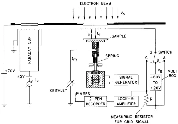
Figure 1. Measurement system.
The beam could be deected from its normal posi-tion so as to incide on the Faraday cup which allowed a precise measurement of the beam current Io. Vac-uum was maintained within the whole system at a pres-sure of 10,6 Torr or less. The grid could be controlled by means of the switch S. In position A the grid was grounded, in position B it could be poled by means of a voltage box with potentials varying from -60 V to + 20 V. In position C it was connected with the resistor R which provided the input for the lock-in amplier men-tioned below. The rear electrode of the sample was con-nected with the Keithley meter K1 which showed the measuring currentImand with the double pen recorder which registered the pulses of secondary electrons and
of the vibrating capacitor (see below).
around EI I. Samples with a positive residual charge are irradiated with a beam of energy above EI Ias discussed in [6].
After compensation, and before any new shot, the surface of the sample was examined whether it was in-deed free of charge. The method of the vibrating capac-itor was used [7]. The xed plate was the grid which was connected to ground (position C of switch S) over the measuring resistor R. The other plate was the surface of incidence of the sample which was mounted on a steel rod which could move within a tubular guide and could be vibrated by a magnetic coil. If the surface of inci-dence of the sample was not fully discharged it would induce voltage oscillations on the xed plate (the grid with the switch in position C) which eventually were indicated by the recorder. We believe we could main-tain the surface of incidence in rest at a potential of at most 0.5V.
The current Im emerging from the rear of the sam-ple was measured by a Keithley meter whose low exit was grounded. The same meter was connected over its rear contact with the recorder which registered the single pulses of the secondary emission. The use of the lock-in-amplier prevented interference between the measurement of the secondary emission and the surface potential of the sample. The beam currentIowas mea-sured by the second Keithley connected to the Faraday cup to which the beam can be deviated. The pulses have a duration of less than half a second. After reach-ing a peak within a very short time, they are seen to decline, but for the amplitude measurements we took their peak values.
III Field - free and eld -
stim-ulated emission
The grid was biased by a external voltage source by a voltageVg which could be varied from a negative mini-mumV
,
g to a positive maximumV +
g :ForV ,
g <Vg<0 one measures the secondaries which have enough energy to overcome the retarding eld set up by Vg. Secon-daries with energies betwen Vg and 0 are turned back by the eld of the grid and return to the surface of incidence. For 0+
Vg < V +
g the eld has inverted direction and becomes attractive. If the sample is a dielectric, the eld extends into the bulk of the mate-rial, energizes secondaries generated by collisions with the penetrating beam, and enables them to travel back to the surface and be emitted. These electrons are the
origin of the current component dened as eld stimu-lated emission. We know that the intensity of the beam changes with depth in the dielectric but here we disre-gard this eect and use the box model, attributing to the incident primaries a constant range which depends only on their energy.
For metals no such eld-stimulated emission exists since the eld collapses within the material. So the section of the beam extending beyond the surface layer does not contribute to the emission, which remains con-stant.
IV Eect of beam voltage
The eld-free emission for negative and zero voltage originates from collisions of the beam with near-surface atoms and is limited to a thin layer (the escape depth). With increasing positive voltageVoof an incident beam current of given intensityIo, the depth of penetration increases (range increase) and the density of ionization-generated electrons along the range decreases. There-fore fewer electrons are available at the surface layer for emission which therefore decreases. Note that for each series of measurements intensity and voltage of the beam remained constant.
The energy spectrum of the eld-free emitted elec-trons extends from zero to the beam energy. Here, fol-lowing practice, we shall be concerned with secondary electrons, that is, those having energy no greater than 50 eV. Therefore, we dene V
,
g =,50V as the maxi-mum negative voltage to which our measurements shall extend; its maximum positive value isV
+
g = +20V.
V Current equation
The emission current Is is the dierence between the measuring current Im and the value of the beam cur-rent Io dened as positive and constant throughout. Generally one has ([8], Eq. 1)
Is=Im,I
0 (1)
VI Electron energy distribution
function
emitted per second, gives the corresponding current el-ement (e=s) g(V)d(V). The expression for Is depends on whether the grid potential is negative or positive. In the rst case one has
Is(Vg) = Z V
g
V, g
(e=s)g(V)dV; V ,
g Vg0 (2) and in the second case
Is(Vg) = Z V
g 0
+
(e=s)g(V)dV; 0 +
VgV +
g (3)
Eqs. (2) and (3) can be combined giving
Is(Vg) = Z V
g
V, g
(e=s)g(V)dV; V ,
g Vg V +
g (4)
Normalizing this equation gives on the left side I
g(s): The right hand term is divided byRV
+ g
V, g
(e=s)g(V)dV: Combining the normalized left-and right-side ex-pressions gives
Is(Vg) = Z V g V, g g (
V)dV; V ,
g VgV +
g (5)
where g
is the normalized distribution function. Derivation and use of Eq. 1 give
g (
Vg) =
dIm(Vg)=dVg Im(V
+
g ),I 0
(6) Nominator and denominator are negative, sog
( V) comes out positive.
VII Experimental results
Metal- The secondary emission current for Platinum (area 7.1 cm2) is shown in Fig. 2 for a beam current of 210
,8 A and voltages of 300 to 4000 V. In all cases the currents become constant when the retarding voltage reaches zero and they remain so for increasing (positive) voltages (0+
<Vg <20V): Therefore there does not exist a stimulated emission from the metal. When the grid voltage becomes negative, the current emission falls fast and for -14V it has come down to 710
,9 A. It depends strongly on the beam voltage V
0, decreasing with increasing values of V
0. The emis-sion current decreases by a factor of 1.7 for a variation of V
0 from 300 V to 4000 V. As explained before the increasing beam range, at constant total beam current, decreases the specic ionization along its range and thus
reduces the number of electrons available for emission at the surface.
Figure 2. Secondary emission current from Platinum as a function of emission voltage, beam current 210
,8A, beam
voltages from 300 V to 4000 V.
The electron energy prole of Platinun for a beam voltage V
0 = 300 V is shown in Fig. 3. The values to the left of eV=0 correspond to collisions between the incident electrons and atoms of the surface layer of the metal. Since the electrons thus generated are freely emitted and are counted provided they overcome the grid, the measured values of g or g
indicate directly the corresponding emission energies and thus give the true energy prole. The prole is strongly peaked with a half width of 2.5 eV, with the peak situated at -4 V, within the eld-free emission. The small section of the curve extending beyond zero is probably due to lack of precision of the measurement and scattered high energy electrons interacting with the grid and chamber walls. The absence of eld stimulated emissions is conrmed.
Insulator- The emission from the insulating poly-mer Teon FEP (uorethylene propylene) is shown in Fig. 4. The incident beam current in this case was 2.5 nA and the beam voltage varied from 200 to 2500 V. The emission current does not become constant and in-dependent on V
g at V
g = 0, but continues to increase straight on to the right of eV = 0 when one reaches pos-itive energy values; since the eld has changed direction and from retarding has become accelerating, additional electrons within the dielectric are returned to the sur-face and maintain the increase of I
s, this time due to the eld-stimulated emission. The decrease of I
s with increasing V
o is explained as before by the decrease of specic ionization with increasing range.
Figure 4. Secondary emission current from Teon FEP as a function of emission voltage. Beam current 2.5 nA, beam voltages between 200 and 2500 V.
Figure 5. Electron energy prole for Teon FEP. Beam cur-rent 2.5 nA, voltage 1000 V.
The corresponding electron energy prole forV o = 1000V is shown in Fig. 5.
The physical interpretation of the two sections of Fig. 5 for dielectrics diers. The left section, as dis-cussed above, gives the true energy values of electrons
originated by collisions with near-surface atoms. But the right side refers to collisions between beam elec-trons and atoms within the material, some distance from the surface. The electrons thus generated, move in the direction of the surface under the inuence of the penetrating electric eld but on the way lose some of their original energy due to conduction and colli-sions and when they arrive at the surface of emission, their energy diers from its original value. Therefore the computed value of g is slighty lower than the true value. The dierence is believed to be small because the distance travelled by the electrons is short and there is indeed no lack of continuity of the curves ofI
s(
g) versus gwhere they cross the surface.
The prole, with a half-width of 4 eV, is much larger than for the metal.
The energy of the eld-free emission decreases with decreasing distance from the emitting surface. How-ever once one enters the region of stimulated emission the energy of the electrons begins to increase again due to the surging accelerating eld. Therefore the energy scale in Fig. 5 decreases from an initial positive value to zero, but subsequently rises again to positive values.
In Figs. 3 and 5, we have replacedV
g by eV, noting that our negative potentials as well as the positive ones correspond to positive kinetic energies.
A series of other measurements with various mate-rials, including PETP and PVDF showed qualitatively the same behavior as described above [5].
VIII Conclusion
The experimental results presented here give evidence that an externally applied positive electric eld extend-ing into a dielectric enhances the secondary electron emission by removing from the bulk of the material electrons generated there by the electron beam. Fur-ther experimental and theoretical developments will be needed for a satisfactory understanding and theory of the eect.
he was the rst to discover eld stimulated emission for very high applied elds and beam energies.
Acknowledgments
One of the authors (B.G.) is greatly indebted to Dr. Frederickson (USAF, Phillips Lab. Hanscom AFB, MA 01731), now at Calif. Inst. Techn., Jet Propulsion Lab., Pasadena, Calif., for having called his attention to his various recent experiments on secondary emission from PMMA shielding material which proved the eect of stimulated emission.
All authors wish to extend their gratitude to Pro-fessor G.F. Leal Ferreira for his help in the completion and organization of the typescript and numerous dis-cussions, and to the special editor of this issue of the Brazilian Journal of Physics, Prof. Dr. R. Gerhard-Multhaupt.
References
1. E. J. Sternglass, Phys. Rev.
95
, 345 (1954). 2. A. Dekker, Secondary Emission. In: SolidPhysics, Academic Press, New York
150
, 251 (1958).3. H. Seiler, J. Appl. Phys.
54
, R.1 - R 18 (1983). 4. H. von Seggern, IEEE Trans. Nuclear Sci.32
,1503 (1985).
5. C.A.F. Pint~ao, PhD Thesis 1996, Institute of Physics of S~ao Carlos, University of S~ao Paulo, S~ao Carlos.
6. R. Hessel, PhD Thesis 1990, Institute of Physics of S~ao Carlos, University of S~ao Paulo, S~ao Carlos. 7. W. A. Zisman, Rev. Sci. Inst.
3
, 361 (1932) L.Kelvin, Phil. Mag.
46
, 82 (1898).8. B. Gross and R. Hessel, IEEE Trans. El. Ins.
26
, 18 (1991).9. A. R. Frederickson and S. Woolf, J. Appl. Phys.