J O U R N A L O F M AT E R I A L S S C I E N C E : M AT E R I A L S I N E L E C T RO N I C S1 5( 2 0 0 4 ) 6 5 7 ± 6 6 3
Dielectric permittivity and loss of CaCu
3
Ti
4
O
12
(CCTO) substrates for microwave devices
and antennas
L. C. KR ETLY
1, A. F. L. AL MEIDA
2, P. B . A. FECHINE
2, R. S. DE OLIVEIRA
3 , 4,
A. S. B . S OMBRA
41
Departamento de Microondas e OÂptica (DMO), Faculdade de Engenharia EleÂtrica e
ComputacËaÄo (FEEC), UNICAMP, Brazil
2
Departamento de QuõÂmica OrgaÃnica e InorgaÃnica, Centro de CieÃncias, UFC, Fortaleza,
CearaÂ, Brazil
3
Departamento de FõÂsica, Universidade Estadual do Ceara (UECE), Fortaleza, CearaÂ, Brazil
4LaboratoÂrio de TelecomunicacËoÄes e CieÃncia e Engenharia dos Materiais (LOCEM),
Departamento de FõÂsica, UFC, Campus do Pici, Caixa Postal 6030-CEP 60.455-760,
Fortaleza CE, Brazil
E-mail: sombra@®sica.ufc.br
The solid state procedure was used to produce bulk ceramics of CCTO (CaCu
3Ti
4O
12). The
samples of the CCTO ceramic were studied by X-ray powder diffraction, infrared and Raman
scattering spectroscopy. The infraredandRaman scattering spectroscopy con®rm the
formation of the CCTO phase as seen by X-ray diffraction analysis. For one experimental
procedure one uses an organic binder in the process of shaping the samples. In the second
procedure the samples were prepared without the presence of the organic phase. For the
secondsituation, we hadhigher dielectric constant (
e
r
7370) with high loss (
D
0.2) at
1 KHz. For the ®rst procedure one has the lower dielectric constant (
e
r
1530) andlower loss
(
D
0.11) at 1 KHz. Simple rectangular antenna prototypes were also designed on substrate
samples (C1, C2, P1 andP2). For the antennas (with P2, C1 andC2 as substrates), the
bandwidth (BW) is 90 MHz (around 3%). The antenna with P1 substrate presented a
surprisingly high BW of 270 MHz that corresponds to a 10% bandwidth. In the microwave
range one observes that higher values of the
e
rin the range of 3 GHz antennas is also
presentedby the P1 sample (
e
r
41.6), andthe lowest one was presentedby P2 (
e
r
33.7).
Sample P1 also presents the highest value for the loss (
Q
1) which is around0.1 comparedto
the other samples which is around0.03. Therefore, these measurements con®rm the
potential use for small high dielectric planar antennas. These materials are also attractive for
capacitor applications andcertainly for microelectronics, andmicrowave devices (e.g., cell
mobile phones), where the miniaturization of the devices is crucial.
#
2004 Kluwer Academic Publishers
1. Introduction
High dielectric constants have been found in oxides of the type CaCu3Ti4O12 [1±3] (CCTO) which shows a dielectric constant e
r
at 1 KHz of about 10 000 that is nearly constant from room temperature to 300C. Oxides with the perovskite structure are well stabilized by their high dielectric constants e
r
which lead these class of materials to a big number of technological applications [4]. However this behavior is generally associated with ferroelectric or relaxor properties. In these cases the highest value ofer is obtained during a phase transition (as a function of temperature) presented by the material. The existence of a transition temperature is generally a problem when one is talking about applications of these materials. The reported results for CCTO shows that the
e
r is high but with small dependence on the temperature [3]. Such materialis very promising for capacitor applications and certainly for microelectronics and microwave devices (e.g., cell mobile phones), where the miniaturization of the devices are crucial.
High e
r ceramics make it possible to noticeably miniaturize passive microwave devices. Their size can typically be reduced in comparing with classical resonators and ®lters by a factor of 1 e
r
p (relative dielectric constant).
technique to obtain any quantity of powder with controlled microstructure [7]. Recently a polymeric citrate precursor route was used to produce CCTO [8]. It was observed that the dielectric constant is about 3000 and loss around 0.3 to 0.35 at 1 KHz.
In this work we report the preparation of the ceramic of CCTO through the solid state route and use the bulk ceramic as a substrate for a planar microwave antenna application. The produced samples were studied using X-ray diffraction, infrared and Raman Spectroscopy techniques. The dielectric constant and loss were studied in the radio frequency (100 Hz to 1 MHz) and in the microwave range.
The production, and the study of the properties of the CCTO ceramics is important in view of possible applications as bulk devices like microwave resonators and oscillators, thick and thin highe
r®lms.
2. Experimental procedures
2.1. Sample preparation
Commercialoxides Ca(OH)2 (Vetec, 97% with 3% of CaCO3), titanium oxide (TiO2) (Aldrich, 99%), CuO (Aldrich, 99%) were used in the CCTO preparation. The material was ground on a Fritsch Pulverisette 6 planetary mill with the proportionality of Ca(OH)2±3CuO±4TiO2. Milling was performed in sealed stainless steel vials and balls under air. Mechanical alloying was performed for 1 h of milling. In this case the milling was used only to give a good homogeneity of the powder. However, we already showed in the literature that for 100 h of milling the complete production of CCTO is possible [6]. The reaction occurring during milling can be summarized as
Ca(OH)23CuO4TiO2 ? Impacts
CaCu3Ti4O12H2O The milled powder was calcinated at temperatures in the range of 900 to 1000C for 12 h. The powder was mixed with an organic binder and compacted into disks at a pressure of 2.5 ton. The pellets were then sintered at 1050C for 24 h. These samples were denominated by C1 and C2 (see Table I). The same powder were prepared
without the organic binder with the same ®ring process. The denomination for these samples will be: samples P1 and P2 (see Table I).
2.2. X-ray diffraction
The X-ray diffraction (XRD) patterns were done using a Siemens D5000 equipment with Cu±Ka radiation in a Bragg±Brentano geometry at room temperature (300 K) by step scanning using powdered samples. We used 5 s for each step size of counting time, with a Cu±Katube at 40 kV and 25 mA.
2.3. Infraredspectroscopy
The infrared spectra (IR) were measured using KBr pellets made from a mixture of powder for each glass composition. The pellet thickness varied from 0.5 to 0.6 mm. The IR spectra were measured from 400 to 1400 cm 1 with a Nicolet 5ZPX FT-IR spectro-meter
2.4. Raman spectroscopy
Micro-Raman measurements were performed using a T64000 Jobin Yvon spectrometer equipped with an N2-cooled charge coupled device (CCD) to detect the scattered light. The spectra were excited with an argon-ion laser (5145 AÊ ). The spectrometer slits were set to give a spectral resolution always better than 2 cm 1. The Raman scattering was measured in a back scattering geometry directly from the powder.
2.5. Electrical measurements
The dielectric and loss measurements were obtained from a HP 4291A Impedance Analyzer, which cover the region of 100 Hz to 100 MHz. The dielectric permittivity
e r
and dielectric loss D measurements, were performed using a parallel plate capacitor arrangement. The samples were formed into thin circular disks with
T A B L E I Radio frequency and Microwave measurements of the samples Sample CCTO(CS) Thicknesse(mm)
Density (g/cm3)
Electrode diameter L(cm)
Dielectric Loss (D) 10 2
De00=e0
1 KHz 1 MHz
Dielectric Constant
ere0=e0
1 KHz 1 MHz
C1 2.61 4.7 11 1530
3.2 35 718
C2 2.29 4.7 11 1641
3.14 37 769
P1 2.12 3.6 20 7370
3.76 34 4271
P2 2.12 4.2 22 7073
3.77 61 3444
Planar antenna measurements
C1 C2 P1 P2
Resonant frequency fR(GHz)
2.95 2.9 2.7 2.9
eeff 25.8 26.7 30.8 25
er 34.8 36 41.6 33.7
diameter around L3 to 5 cm and thickness around
e2 mm (see Table I). The Ag (circular electrodes) were screen printed at each surface and ®red at 400C for 1 h. The resonance measurements in the range of 0.3 to 3 GHz range was done in a conventionalset up, measuring the S11 parameter using a HP 8714ET Network Analyzer (see Section 2.6).
2.6. Model for microstrip radiator
The test structure used for dielectric constant measure-ments is a resonant-style radiator shown in Fig. 7(a) and (b). The patch antenna is fed by a microstrip line in direct contact to the patch conductor of lengthLand widthW. There are several models related to the planar patch antenna analysis. Among them are: transmisson line model, cavity model and full-wave analysis [12]. Microstrip antennas resemble dielectric loaded cavities. A well-accepted model detailed in Refs. [12, 13]. Due to the ®eld con®guration at the edges, the antenna has two radiation edges and two resonant edges. The radiation of the antenna takes place from the two slots comprising between theWedges and ground plane. TheLedges are the resonant dimensions (See Fig. 7(a)). The transmis-sion line model approaches the microstrip antenna as two slots separated by a low impedance transmission line (the patch) of lengthL. For the dominant mode TM010which is the dominant mode with the lowest frequency, the resonant frequency is given in Ref. [12]:
fr
c
2 L2DL e reff
p 1
where DL is the additional line length to account the fringing ®elds which has a practical approximation given by [12]:
DL
h 0:412
ereff0:3
W=h 0:264 ereff 0:258
W=h 0:8 2
and the ereff is the effective dielectric constant (where effective means a composite value of the overall dielectrics in the system which involves the dielectric constant of materialitself and the air). In general 15ereff5er. The fringing effects on the microstrip gives:
ereff W er1
2
er 1
2 F W =h 3 and
F W=h
112h=W 1=20:04 1 W=h2;
W=h1
112h=W 1=2; W=h1
8 <
:
4 For the measurements in this work we have used a square microstrip antenna withWL1 cm.
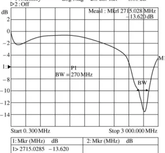
The resonant frequency is precisely measured using a network analyser and measuring the return loss (in dB) through theS11scattering parameter of the antenna under test. The very precise resonant frequency identi®cation is done trough the lowermost point in the S11 curve (see Fig. 8). TheS11 test is the main test for antennas. This parameter shows the re¯ections of the signalat the feeding point, the entrance of the antenna. High negative
values (typically between 12 and 40 dB) in the dip (see Fig. 8) indicate that the electromagnetic waves were not re¯ected. It means that the antenna is radiating. In the
10 dB line, there is an antenna bandwidth, BW, (almost equalto VSWR: 2 : 1). With this data the antenna personnelmight be able to estimate the radiation performance to a certain degree.
Theer value is extracted from the expressions above with the correction related to the fringing ®elds. There are other methods for er measurements but this one is straightforward because the test structure is close to the ®nalapplication structure.
Essentially e
r is determined from the resonant frequency atfRandQ 1 (the loss factor) is determined fromDf=f
R , whereDf(BW) is the 10 dB bandwidth of the resonance (see Table I).
3. Results and discussion
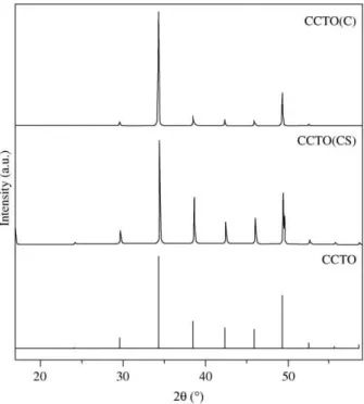
The X-ray diffraction of the ceramic after calcinations CCTO (C) and calcinationsinterization CCTO(CS) are shown in Fig. 1. After calcination the CCTO phase is easily identi®ed. The diffraction pattern of the sample CCTO(CS) (see Fig. 1) does not change much after the sintering procedure.
In Fig. 2 one has the Raman spectra of the calcined CCTO(C) and sinterized samples CCTO(CS) where the three main peaks at 445, 508 and 572 cm 1 is easily identi®ed. Assignment of the Raman spectralfeatures to the crystalline CCTO has been reported previously [2, 9]. Scattering peaks at 445, 513 and 572 cm 1 were observed [2]. In Ref. [9] the Raman lines at 445 and 511 cm 1were associated with the Ag symmetry (TiO
6 rotationlike) and 575 cm 1 of Fg symmetry (O±Ti±O anti-stretching). The agreement between the previous Raman results for CCTO with our samples obtained by sintering process is good.
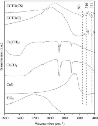
In Fig. 3 one has the IR spectra of the ceramics
CCTO(CS) and CCTO(C) together with the spectra of the starting materials. One can notice that the CCTO phase present resonance absorptions at 561, 516 and 441 cm 1 for CCTO(CS). Severalauthors have assigned [10] this region of absorptions with the titanium ion. These bands were associated to nTi±O 653 550 cm 1 and
nTi±O±Ti 495 436 cm 1.
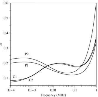
In Figs. 4 and 5 one has the dielectric permittivity e r of all the samples (C1, C2, P1 and P2) in the range of 100 Hz to 1 MHz. For all the samples there is a decrease of thee
r value for this range of frequency. For samples C1 and C2 the value at 100 Hz, e
r*1800 decreases to 800 at 1 MHz. For samples P1 and P2, where we did not use any organic binder, the dielectric constant was higher. For samples P1 and P2 the value at 100 Hz, er*10 000 decreases to 4000 at 1 MHz. We believe that the presence of the organic phase is playing a critical effect in the grain size and boundaries which is affecting the effective dielectric constant of the ceramic [8]. The organic phase (low-dielectric constant) in association with the CCTO grains (high-dielectric constant) is leading to lower dielectric constant composite. In Fig. 6 one has the dielectric loss for all the samples. At low frequencies the samples P1 and P2 present higher losses compared to C1 and C2 samples. The loss is increasing with the frequency and is around 0.35 for samples C1 and C2 around 1 MHz. In Table I one has the dielectric constant and loss for all the samples at 1 KHz and 1 MHz. The increase of the loss for all the samples with frequency was reported in the literature by others authors [8]. To investigate the potentialapplication of the CCTO materials for microwave planar devices, a series of planar microstrip antennas were done. The demand for new mobile communication systems will push hard to miniaturization and low volume devices and equipment. Due to these requirements in portable, or repeater stations in a mobile communication for cellular systems, for example, high dielectric constant materials can be used to effectively reduce the size of planar microstrip antennas [11].
The performance of a planar antenna is related to theL
andWdimensions of the patch and the dielectric constant e
r of the substrate. For the best compromise between antenna gain, ef®ciency, bandwidth and volume, an adequate materialwith a higher must be found for low volume. Of course, there is a trade off: high dielectric constant materials give a low volume antenna but it imposes low bandwidth and gain. Moreover, there is a
Figure 2 Comparison of the Raman Spectra of the calcinated sample CCTO(C) and calcinatedsintered sample CCTO(CS).
Figure 3 Comparison of the Infrared Spectra of the calcinated sample CCTO(C) and calcinatedsintered sample CCTO(CS) with the starting materials.
Figure 4Dielectric Constant e
demand for monolithic integration of antennas and associated circuitry and these requirements claim compatible high dielectric constant materials.
The simple rectangular antenna prototypes were designed on substrate samples with nominally 3±4 cm in diameter and 2±3 mm thick (see Table I). The resonant frequency fR was calculated in the range of 2±3 GHz, based on the dielectric constant available data (1±3.8). One of the experimentalantennas is shown in Fig. 7 (sample C1).
All the samples show the electromagnetic radiator potentialproperties, that is, antenna. This is proved when the dips in theS11measurements reach lower values than
10 dB.
The 10 dB point in theS11parameter corresponds to a VSWR of 2 : 1. The S11 parameters for the antennas (return loss) were measured, and the results are shown in Fig. 8 for the P1 antenna. The VSWR52 : 1 ( 10 dB line) criterion was used to identify the antenna bandwidth
and the dip in theS11 measurement (see Fig. 8) below 10 dB is a preliminary indicator of the electromagnetic radiation properties of the device.
As a typicalresult, 90 MHz of bandwidth (BW) was found for the antennas (with P2, C1 and C2 as substrates), which is lower than typical rectangular patch antennas with low dielectric constant substrates, about 3%. The antenna with P1 substrate presented a surprisingly high BW of 270 MHz that corresponds to 10% bandwidth at 3 GHz. Such value is in accordance to the requirements for planar antennas for a variety of wireless communication systems such as WLAN, PCS, Wi±Fi and other protocols. Therefore, these measure-ments con®rm the potentialuse of such materials for small planar high dielectric antennas (HDA).
In Table I one has also the values of thee
r (at radio frequency and in the microwave region)eeff (effective dielectric constant), dielectric lossDand the loss factor Q 1(obtained from theS11and is given byQfR=BW). One can conclude that the higher values of thee
r in the range of 3 GHz antennas is also presented by the P1 sample. The value of the dielectric constant for this sample is around 41 (see Table I). This sample also presents the highest value for the loss Q 1which is around 0.1 compared to the other samples which is around 0.03. The same behavior observed at low frequencies, that the higher dielectric constant is also associated to the higher loss is also present in the microwave region.
The low Q 1
values at microwave frequencies
Figure 5 Dielectric Constant er of samples P1 and P2 in the frequency range of 100 Hz to 1 MHz.
Figure 6 Dielectric Loss (Dtga) of samples C1, C2, P1 and P2 in the
frequency range of 100 Hz to 1 MHz.
compared to the low frequency ones (see D measure-ments on Table I), could be associated to a possible additional contribution to the dielectric constant and loss resulting from orientational polarization present at the radio frequency region of the spectra. We have to emphasize that the loss factor obtained in the present device is associated to an open cavity. In this case the substrate loss and the radiating loss are operating together. In summary, the CCTO samples present higher e
r for the samples prepared without any organic binder (e
r7370, 7073 for P1 and P2 respectively at 1 KHz) compared to the samples prepared with the organic phase (e
r1641, 1530 for C1 and C2, respectively, at 1 KHz), respectively, see Figs. 4 and 5 and Table I. The presence of the organic phase could be used to control the value of the DC and loss of the material. However the loss is still a problem to be overcome if one is concerned for applications in the microwave region.
The quality factor Q [12, 13] and bandwidth are antenna ®gures-of-merit that is representative of the antenna losses. Typically there are radiation, conduction (ohmic), dielectric and surface wave losses [12]. The fractionalbandwidth Df of the antenna is inversely proportionalto theQof the antenna, and is given by [13]:
Df
fR 1
QBW 5
Therefore, the bandwidth is inversely proportional to the
Q factor. The performance of a planar microstrip antenna, that uses the CCTO ceramic as a high er substrate was examined. Simple rectangular antenna prototypes were designed on substrate samples (C1, C2, P1 and P2, see Table I). For the antennas (with P2, C1 and C2 as substrates), the bandwidth (BW) is 90 MHz (around 3%). The antenna with P1 substrate presented a surprisingly high BW of 270 MHz that corresponds to a 10% bandwidth at 3 GHz. Such value is in accordance to the requirements for planar antennas for a variety of
wireless communication systems such as WLAN, PCS, Wi±Fi and other protocols. Therefore, these measure-ments con®rm the potentialuse of such materials for small high dielectric planar antennas (HDA).
In the microwave range one observes that higher values of thee
r in the range of 3 GHz antennas is also presented by the P1 sample. The value of the dielectric constant for this sample is around 41. Lower value were presented by sample P2 (33.7). Sample P1 also presents the highest value for the loss Q 1which is around 0.1 compared to the other samples which is around 0.03. The same behavior observed at low frequencies, that the higher dielectric constant is also associated to the higher loss is also present in the microwave region. These materials are also very promising for capacitor applica-tions and certainly for microelectronics, and microwave devices (e.g., cell mobile phones), where the decrease of the size of the devices are critical.
4. Conclusions
In conclusion, the traditional ceramic procedure (solid state procedure) was used to produce bulk ceramics of CCTO (CaCu3Ti4O12). The samples of the CCTO ceramic were studied by X-ray powder diffraction, infrared and Raman scattering spectroscopy. After 30 h of milling the formation of CCTO was con®rmed by X-ray powder diffraction. The infrared and Raman scattering spectroscopy con®rm the formation of the CCTO phase as seen by X-ray diffraction analysis. For one experimentalprocedure one uses an organic binder in the process of shaping the samples. In the second procedure the samples were prepared without the presence of the organic phase. For the second situation we had higher dielectric constant e
r7370
with high
loss D0.2at 1 KHz. For the ®rst procedure one has the lower dielectric constant e
r1530
and lower loss D0.11 at 1 KHz. Rectangular antenna prototypes were also designed on substrate samples (C1, C2, P1 and P2). For the antennas (with P2, C1 and C2 as substrates), the bandwidth (BW) is 90 MHz (around 3%). The antenna with P1 substrate presented a surprisingly high BW of 270 MHz that corresponds to a 10% bandwidth at 3 GHz. Such value is in accordance with the require-ments for planar antennas for a variety of wireless communication systems such as WLAN, PCS, Wi±Fi and other protocols.
In the microwave range one observes that higher values of thee
r in the range of 3 GHz antennas is also presented by the P1 sample. The value of the dielectric constant for this sample is around 41. Lower value were presented by sample P2 (33.7). Sample P1 also presents the highest value for the loss Q 1which is around 0.1 compared to the other samples which is around 0.03. The same behavior observed at low frequencies, that the higher dielectric constant is also associated to the higher loss, is also present in the microwave region.
Therefore, these measurements con®rm the potential use of such materials for small planar antennas. These materials are attractive for capacitor applications and certainly for microelectronics, and microwave devices (e.g., cell mobile phones), where the miniaturization of the devices is crucial.
Acknowledgments
This work was partly sponsored by Ericsson EDB, Ericsson Research Center Brazil, under contracts Ericsson/UFC-06 and UNI.15/00 and by FINEP, CNPq, FUNCAP, CAPES (Brazilian agencies). We also thank A. G. Souza Filho for the Raman Measurements.
References
1. M . A . S U B R A M A N I A N,D . L I,N . D U R A N,B . A . R E I S N E Rand
A . W. S L E I G H T,J. Solid State Chem.151(2000), 323. 2. A . P. R A M I R E Z, M . A . S U B R A M A N I A N, M . G A R D E L, G .
B L U M B E R G,D . L I,T. V O G TandS . M . S H A P I R O,Solid State Comm.115(2000), 217.
3. M . A . S U B R A M A N I A NandA . W. S L E I G H T,Solid State Sci.4
(2002) 347.
4. N . S E T T E R and E . L . C O L L A, ``Ferroelectric Ceramics'', (Birkhauser Verlag, Basel, 1993).
5. B . B O C H U,M . N . D E S C H I Z E A U XandJ . C . J O U B E R T,J. Solid State Chem.29(1979) 291.
6. A . F. L . A L M E I D A,R . S . D E O L I V E I R A,J . C . G OÂ E S,J . M . S A S A K I,J . M E N D E S F I L H OandA . S . B . S O M B R A,Mater Sci. Eng. B96(2002) 275.
7. R . S . D E F I G U E I R E D O,A . M E S S A I,A . C . H E R N A N D E Sand
A . S . B . S O M B R A,J. Mater Sci. Lett.17(1998) 449.
8. P. J H A,P. A R O R A,A . K . G A N G U L I,Mater Lett.4179(2002) 1. 9. N . KO L E V,R . P. B O N T C H E V,A . J . J AC O B S O N,V. N . P O P O V,
V. G . H A D J I E V,A . P. L I T V I N C H U K,M . N . I L I E V,Phys. Rev. B
66(2002) 132102.
10. S . M U S I C, M . G O T I C, M . I VA N D A, S . P O P O V I C, A . T U R KO V I C,R . T R O J KO,A . S E K U L I C andK . F U R I C,Mater Sci. Eng. B47 (1997) 33.
11. B . L E E, F. J . H A R AC K I E W I C Z, IEEE Trans. on Antennas Propagat.50(2002) 1160.
12. E . A . B A L A N I S, ``Antenna Theory ± Analysis and Design'', 2nd edn. (John Wiley and Sons New York, 1997).
13. R . G A R G, P. B H A R T I A, I . B A H L and A . I T T I P I B O O N, ``Microstrip Antenna Design Handbook'' (Artech House, Norwood, MA, 2001).