University of Algarve
Thermally Stimulated Currents On
Oxide Based TFTs
Fábio Emanuel Sousa Cabrita
Dissertation
Master degree in
Electronic and Telecommunications Engineering
Work done under the supervision of: Prof. Dr. Henrique Leonel Gomes
Fábio Emanuel Sousa Cabrita
v. 1.1
Thermally Stimulated Currents On
Oxide Based TFTs
Dissertation present to a jury of the University of Algarve on Gambelas Campus has requirement to obtain the title of Master Degree on Electronic and Telecommunication Enginneering, with the supervision of Prof. Dr. Henrique Leonel Gomes.
“The top of one mountain is always the bottom of another.” Marianne Williamson
i
STATEMENT OF ORIGINALITY
Statement of authorship
I declare that I am the author of this work that is original and unpublished. Authors and consulted works are properly identified on the text, and are included on the list of references.
____________________________________
(Fábio Cabrita)
Copyright © Fábio Cabrita.
The University of Algarve have the right, perpetual and without geographical boundaries, to record and publish this work with copies printed in paper or in digital format, or with other mean known or that will be invented, to share it on scientific repositories and to have his own copy and distribution with education or investigation with non-commercial purposes, since the credit must be given to the author and the editor.
ii
AGRADECIMENTOS
Em primeiro lugar, ao Professor Doutor Henrique Gomes, pela oportunidade que me deu e por me ter orientado nesta dissertação de Mestrado, com criticas fundamentais, partilha de conhecimentos, e por todo o apoio que me que foi dado nesta jornada.
À equipa do CENIMAT, mais propriamente à Asal Kiazadeh e à Daniela Salgueiro, por terem partilhado as suas amostras connosco, pela sua paciência e todo o apoio que me deram no decorrer desta dissertação.
De seguida, queria também agradecer a todos os meus amigos e colegas, que já tinha, e que fiz tanto no decorrer da dissertação como no meu percurso académico em geral, por todos os bons e menos bons momentos de divertimento e trabalho que passamos juntos, pelo apoio e ajuda que me deram, e que já mais irei esquecer.
No fim, mas não menos importantes, queria agradecer em especial à Minha Namorada e à Minha Família, em especial aos meus Pais e aos Meus Avós, por todo o apoio que me deram pois sem eles nunca teria conseguido chegar onde cheguei, a eles um grande obrigado por terem confiado em mim.
iii
ACKNOWLEDGMENTS
First of all, to Professor Henrique Gomes, for the opportunity that he gave me and for having guided me in these Master dissertation, with fundamental criticism, knowledge sharing, and for all the support that was given to me on this journey.
The team CINEMAT, more precisely to Asal Kiazadeh, and Daniela Salgueiro, by sharing their samples with us, and for the patience and all the support that they have gave me during this dissertation.
Then, I also wanted to thank all my friends and colleagues, who already had, and did, both during the dissertation as in my academic life in general, for all the good and less good moments of entertainment and work spent together, for their support and help they gave me, and that I will never forget.
In the end, but not less important, I also wanted to thank, specially to My Girlfriend and My Family, specially to My Parents and My Grandparents, for all the support that they gave me because without them I would never have managed to get where I am, to them a big thank you for trusting me.
iv
RESUMO
Óxidos amorfos semiconductores têm assumido um papel de liderança para aplicações em Transístores de Filme Fino (TFTs). Este tipo de transístores tem aplicações em ecrãs planos que usam Díodos Emissores de Luz (LEDs). Os TFTs controlam a activação de cada pixel luminoso. Em teoria os óxidos semiconductores podem ser fabricados em substratos de grandes dimensões, e eventualmente num futuro próximo, em substratos flexíveis de baixo custo, como o plástico e o papel. Esta possibilidade torna esta tecnologia um competidor direto com a electrónica orgânica, em particular onde o desempenho e o custo são um requisito essencial.
Esta dissertação apresenta a caracterização eléctrica de um conjunto de Transístores de Efeito de Campo (FET) com base em filme finos de óxidos amorfos. Apresenta os métodos de fabrico, os materiais usados, estrutura física, modo de funcionamento e as características eléctricas.
TFTs com base em óxidos semiconductores sofrem de um conjunto de problemas que afectam o seu desempenho. Uma das instabilidades é a alteração das propriedades eléctricas quando expostos à luz. Este problema é tanto mais grave já que umas das aplicações dos TFTs é justamente em ecrãs.
O objectivo principal desta dissertação é identificar a origem física da instabilidade à luz. Com este objectivo usou-se um conjunto de técnicas eléctricas desenhadas para obter informação sobre os estados electrónicos que são induzidos quando o TFT é exposto à luz. Um das técnicas usadas foi o método das Correntes Termo Estimuladas (TSC).
O óxido semiconductor em estudo foi o Zinc Tin Oxide (ZTO).
Os resultados obtidos permitiram concluir que a luz induz um estado electrónico no semiconductor. Este estado electrónico comporta-se como um dopante e aumenta a condutividade eléctrica do material. As TSCs permitiram ainda identificar que este dopante esta energeticamente localizado a 0.14 eV da banda de condução do semicondutor. O estado induzido pela luz é muito mais raso que o estado responsável pela condução eléctrica normal, quando o TFT não é exposto à luz. TFTs não expostos à luz mostram um processo de condução termicamente ativado mas com uma energia de activação de 0.22 eV.
v
Os estados electrónicos induzidos pela luz tem um tempo de vida de algumas horas. Este tempo de vida é suficientemente longo para considerar a possibilidade de usar este efeito em foto-sensores do tipo Charge-Coupled Devices (CCD) ou em memórias ópticas. Desta forma um efeito que é prejudicial pode ser convertido numa aplicação prática.
Palavras-chave: Transístores de Óxidos de Filme Fino; Transístor de Efeito de Campo; Caracterização Elétrica de Transístores; Correntes Termicamente Estimuladas.
vi
ABSTRACT
Amorphous oxides semiconductors have played a leading role for applications in Thin-Film Transistors (TFTs). This type of transistor has applications in flat panel displays that use Light Emitting Diodes (LEDs). The TFTs control the activation of each light pixel. In theory the oxide semiconductor can be fabricated on large substrates, and in the near future on low cost flexible substrates such as plastic and paper. This makes this technology a direct competitor with the organic electronics, particularly where performance and cost are an essential requirement.
This dissertation provides an electrical characterization of a set of Field Effect Transistors (FET) based on thin films of amorphous oxides. It presents methods of manufacturing, materials used, the physical device structure, and electrical characteristics.
TFTs based in semiconducting oxides suffer from a number of problems affecting their performance. A well-know instability is the change of electrical properties when exposed to light. This problem is serious because some of the applications of TFTs are precisely on TV screens.
The main objective of this dissertaion is to identify the physical origin of this instability to light. For this purpose we use a set of electrical techniques that can provide information about the electronic states induced when the TFT is exposed to light. One of these techniques used is Thermal Stimulated Currents (TSC).
The semiconducting oxide studied was Zinc Tin Oxide (ZTO).
The results showed that light induces an electronic state in the semiconductor. This electronic state behaves as a dopant and increases the electrical conductivity of the material. TSCs shows that this dopant is energetically located to 0.14 eV of the conduction band of the semiconductor. The light-induced state is shallower than the state responsible for the normal TFT conduction, when the TFT is not exposed to light. TFTs not exposed to light show an electrical conduction mechanism that is thermal activated with an activation energy of 0.22 eV. The electronic state induced by light has a lifetime of several hours. This is long enough to consider the possibility of using this effect in photo-sensors such as Charge-Coupled-Devices
vii
(CCD) or in optical memories. Thus an effect that is detrimental can be converted into a practical application.
Keywords: Oxide Thin film Transistors; Field Effect Transistor; Electrical Characterization of Transistors; Thermal Stimulated Currents.
viii
CONTENTS
STATEMENT OF ORIGINALITY ... I AGRADECIMENTOS ... II ACKNOWLEDGMENTS ... III RESUMO ... IV ABSTRACT ... VI CONTENTS ... VIII LIST OF FIGURES ... X INDEX OF TABLES ... XII NOMENCLATURE ... XIIICHAPTER 1. INTRODUCTION ON OXIDE BASED THIN-FILM TRANSISTORS .. 1
1.1. General Introduction on Field Effect Transistors ... 2
1.2. Methods of Fabrication... 3
1.3. Materials of Layers ... 10
1.4. Device Structure ... 11
1.5. Operation and Parameters... 13
CHAPTER 2. THERMAL STIMULATED CURRENTS ON TFTS ... 18
2.1. Thermal Stimulated Currents ... 19
CHAPTER 3. EXPERIMENTAL ... 23
3.1. Assembly of the Equipment ... 24
3.2. Short Description of the Individual Equipment and Specifications ... 27
CHAPTER 4. ELECTRIC CARACTERIZATION OF ZTO BASED TFTS ... 32
4.1. Characteristics and Parameters ... 33
4.2. Characterization of TFTs With Urea ... 34
4.3. Characterization of TFTs Without Urea ... 36
ix
CHAPTER 5. STIMULATED CURRENTS ON ZTO TFTS WITH UREA ... 39
5.1. Trap Filling With Light ... 40
5.2. Thermal Stimulated Currents ... 41
5.3. Discussion... 46
5.4. Conclusion ... 48
x
LIST OF FIGURES
FIG. 1.1 - SCHEMATIC OF A VACUUM EVAPORATION SYSTEM. ... 4
FIG. 1.2 - SCHEMATIC OF A SPUTTERING SYSTEM. ... 5
FIG. 1.3 - SCD STAGES: (A) MATERIAL DEPOSITION ON THE SURFACE OF THE SUBSTRATE, (B) SPIN-UP, (C) SPIN-OFF AND (D) EVAPORATION. ... 7
FIG. 1.4 - DCD STAGES: (A)(B) BATH OF THE SUBSTRATE ON THE PRECURSOR, (C)(D) SUBSTRATE REMOVAL OF RESERVOIR AND PRECURSOR DRAIN OUT AND (E)(F) EVAPORATION OF SOLVENTS. ... 8
FIG. 1.5 - SCHEMATIC OF PIEZOELECTRIC INKJET PRINTING SYSTEM [23]. ... 8
FIG. 1.6 - SCHEMATIC OF THERMAL INKJET PRINTING [24]. ... 9
FIG. 1.7 - SCHEMATIC OF A CIJ [24]. ... 10
FIG. 1.8 - COPLANAR CONFIGURATION WITH (A) BOTTOM GATE AND (B) TOP GATE [33]. ... 11
FIG. 1.9 - STAGGERED CONFIGURATION WITH (A) BOTTOM GATE AND (B) TOP GATE [33]. ... 12
FIG. 1.10 - STAGGERED BOTTOM GATE TFT: (A) TOP VIEW AND (B) CROSS SECTION VIEW. ... 12
FIG. 1.11 - CROSS VIEW OF ACCUMULATION MODE ON A STAGGERED BOTTOM GATE TFT [36][1]. ... 13
FIG. 1.12 - ILLUSTRATION OF THE CHANNEL REGION STATES. ... 14
FIG. 1.13 - CHARACTERISTICS OF THE I-V CHARACTERISTICS OF A P-TYPE SEMICONDUCTOR WITH ACCUMULATION MODE. ... 15
FIG. 1.14 - CHARACTERISTICS OF THE TRANSFER FUNCTION CURVE OF A P-TYPE TFT WITH ACCUMULATION MODE. ... 16
FIG. 2.1 - REPRESENTATION OF TSC CURVES MEASURED FROM AN OTFT ... 20
FIG. 3.1 - SCHEMATIC DIAGRAM SHOWING THE ELECTRICAL CONNECTIONS ON THE TFT. ... 24
FIG. 3.2 - SCHEMATIC REPRESENTATION OF A TFT CONNECTED AS A CAPACITOR TO MEASURE TSCS. ... 25
FIG. 3.3 - SCHEMATIC OF THE ENTIRE EXPERIMENTAL SET-UP ON THE CRYOSTAT CHAMBER. ... 27
FIG. 3.4 - PHOTOGRAPH OF THE (A) VARIAN SD-201 AND THE (B) VARIAN TURBO-V 70. ... 28
FIG. 3.5 - PHOTOGRAPH OF EUROSEP INSTRUMENTS XENON DC 75-300. ... 28
FIG. 3.6 - PHOTOGRAPH OF THE (A) HORIBA TRIAX 320 SPECTROGRAPH AND THE (B) FL-1039. ... 29
FIG. 3.7 - PHOTOGRAPH OF THE OXFORD INTELLIGENT TEMPERATURE CONTROLLER. ... 29
FIG. 3.8 - PHOTOGRAPH OF THE KEITHLEY 6487. ... 30
FIG. 3.9 - PHOTOGRAPH OF THE KEITHLEY 487. ... 30
FIG. 3.10 - PHOTOGRAPH OF THE CRYOSTAT CHAMBER USED. ... 31
FIG. 4.1 - ILLUSTRATION OF A SIO2+ZTO TRANSISTOR. ... 33
FIG. 4.2 - PHOTOGRAPH OF A WAFER OF NINE SIO2+ZTO TRANSISTORS WITH EACH RATIO PER TRANSISTOR. THE DIMENSIONS W AND L ARE IN MICROMETERS. ... 33
xi
FIG. 4.3 - I-V CHARACTERISTICS OF THE OXIDE BASED TFT WITH UREA LABELED D5. ... 35
FIG. 4.4 - TRANSFER FUNCTION ON LINEAR REGION OF THE OXIDE BASED TFT WITH UREA D5. ... 36
FIG. 4.5 - I-V CHARACTERISTICS OF THE OXIDE TFT WITHOUT UREA LABELED D9. ... 37
FIG. 4.6 - TRANSFER FUNCTION ON LINEAR REGION OF THE OXIDE TFT WITHOUT UREA D9. ... 38
FIG. 5.1 - PHOTO-GENERATED CURRENT ON A ZTO TFT AS FUNCTION OF THE WAVELENGTH. ... 40
FIG. 5.2 - LIGHT INDUCED CHANGES ON THE LINEAR TRANSFER CURVES. (I) THE TRANSFER CURVES BEFORE AND (II) AFTER 1000 SECONDS OF LIGHT EXPOSURE. BOTH TRANSFER CURVES WERE MEASURED IN THE LINEAR REGION (VDS = 0.25 V). ... 41
FIG. 5.3 - HEATING RAMP USED DURING THE THERMAL DETRAPPING CURRENTS. THE HEATING RATE IS 1.08 K/MIN. ... 42
FIG. 5.4 - THERMAL STIMULATED CURRENT: (I) CURVE RECORDED WITHOUT LIGHT FILLING (BASE LINE) AND (II) CURVE RECORDED AFTER LIGHT FILLING AT ROOM TEMPERATURE FOR 1000 SECONDS. ... 43
FIG. 5.5 - THE EFFECT OF APPLYING GATE BIAS ON THE SHAPE OF THE TSC CURVE: (I) CURVE RECORDED WITH GATE BIAS OF 0 V AND (II) CURVE RECORDED WITH A GATE BIAS OF 2 V. ... 44
FIG. 5.6 - SEMILOG-PLOT OF THE EXPONENTIAL RISE IN CURRENT OBSERVED IN FIG. 5.4. THE TEMPERATURE RANGE USED IS 260-350 K. THE FITTING TO THE CURVE PROVIDES AN ACTIVATION ENERGY OF 0.14 EV. ... 45
FIG. 5.7 - TEMPERATURE DEPENDENCE OF THE TRANSISTOR CURRENT MEASURED IN THE LINEAR REGION (VG = 0 V AND VDS=0.25 V): (I) BEFORE LIGHT ILLUMINATION AND (II) AFTER LIGHT ILLUMINATION. ... 46
FIG. 5.8 - SCHEMATIC OF A BAND DIAGRAM (NOT TO SCALE) OF ELECTRONIC LEVELS IN THE BAND GAP OF THE ZTO. ... 48
xii
INDEX OF TABLES
xiii
NOMENCLATURE
AAV Anodic Arc Vaporization
Al Aluminium
Au Gold
CAV Cathodic Arc Vaporization
CCD Charge-Coupled Device
CD Chemical Deposition
CFM Cubic Feet Per Minute
CIJ Continous Inkjet Printing
CSD Chemical Solution Deposition
CVD Chemical Vapor Deposition
DCD Dip Coating Deposition
D-device Depletion Mode
DOD Drop On Demand
FET Field-Effect Transistor
ELR Extrapolation in the Linear Region
GIZO / IGZO Gallium Indium Zinc Oxide
HfO2 Hafnium Oxide
IAD Ion-Assisted Deposition
𝑖𝐷 Drain Current
𝑖𝑜𝑓𝑓 Off-State
𝑖𝑜𝑛 On-State
IGFET Insulated-Gate Field-Effect Transistor
IP Ion Plating
xiv
ITC Intelligent Temperature Controller
ITFT Inorganic Thin-Film Transistor
ITO Indium Tin Oxide
IZO Indium Zinc Oxide
JFET Junction Field-Effect Transistor
K Kelvin
LED Light Emitting Diode
MESFET Metal-Semiconductor Field-Effect Transistor
Mo Molybdenum
MOSFET Metal-Oxide Semiconductor Field-Effect Transistor
OITFT Hybrid Thin-Film Transistor
OTFT Organic Thin-Film Transistor
PD Physical Deposition
PDAV Plasma Duct Arc Vaporization
PEN Polyethylene Naphthalate
PES Polyethersulfone
PET Polyethylene Terephthalate
PVD Physical Vapor Deposition
SCD Spin Coating Deposition
Si Silicon
SiO2 Silicon Dioxide
SiOxNy Silicon Oxy Nitride
TFT Thin Film Transistor
Ti Titanium
TiO2 Titanium Dioxide
𝑣𝐷𝑆 Drain-to-Source Voltage
xv
𝑣𝐺𝑆 Gate-to-Source Voltage
Vth Threshold Voltage
VLSI Very-Large-Scale Integrated
W Watt
Y2O3 Yttrium Oxide
ZrO2 Zirconium Oxide
1
CHAPTER 1.
INTRODUCTION ON OXIDE BASED
THIN-FILM TRANSISTORS
In this chapter will be exposed some highlights about the family of field effect transistors, as well as some methods of fabrication used nowadays by the industry to produce thin film transistors. It will be also mentioned several materials present on oxide TFTs and their layer disposal. Further will be referenced operation modes and parameters of field effect transistors.
2
1.1. GENERAL INTRODUCTION ON FIELD EFFECT TRANSISTORS
Thin-Film Transistors are a category of Field-Effect Transistors (FET). There are many kinds of FETs types, such as: Junction FET (JFET), Metal-Semiconductor FET (MESFET), Heterostructure FET (HFET) and Metal-Oxide Semiconductor Field-Effect Transistor (MOSFET).The Metal-Oxide Semiconductor Field-Effect Transistor (MOSFET), also known as Insulated-Gate Field-Effect Transistor (IGFET), is quite similar with Thin Film Transistors (TFTs) in terms of layers structure and operation. They got extremely popular since late 1970s, because of his size is quite small comparing with other non FET types used on that time, and the manufacturing process is relatively simple. Because of their applications on digital and analog circuits has memory functions, diodes, resistors and capacitors. Thanks to this, most Very-Large-Scale Integrated (VLSI) circuits are made nowadays using MOSFETs [1][2].
There are three categories of FET transistors within TFTs, the organics, the inorganics and the hybrids that are half organics and half inorganics. The TFTs are now elements of our daily life, working on electronics and photonic products. Now, more than ever, portable communication, computing and identification devices need light weight, high resolution images, transparency, thin size, low power consumption, low power flat panel displays, sensors and TFTs can solve that.
The Organic Thin-Film Transistor (OTFT) is a special kind of Field-Effect Transistor (FET) which is a promising device for the future, based on low-cost materials and fabrication methods, with light weight, mechanical flexibility and transparency. It is suitable with applications that require large area coverage, structural flexibility and low cost which was not possible yet with crystalline Silicon (Si), used for example on mass production of solar cells. They can be integrated on flexible plastic substrates and in rugged surfaces. Performance and reliability are depended on the print process and method. The OTFT brings an opportunity also to print electronics because his fabrication methodology has improved in past years, and will find use in numerous low-cost, large-area applications such as smart cards, flexible displays, mobile phones and inventory tags, flexile integrated circuits, sensors and other future products [3][4].
3
Within Inorganic TFT (ITFT), there is the Oxide TFTs, who are a direct derivation from MOSFETs technology. They have long term reliability compared with the OTFTs. They are also based on low-cost materials and fabrication methods. Inorganics can be printed by ink-jet process, but so far just with a few inorganic materials. Printable inorganics is a new process comparatively with organics. Improvements have been done to achieve the same flexibility as the organics. Since OTFTs lacks on performance, have low mobility and low current density, it is expected that ITFTs could replace OTFTs in the near future on certain applications like displays for example [5][6].
The Hybrid TFT (OITFT), promise the advantageous of the organics and inorganics, such as the component of organics on self-assembly and transparency ability, and the component of the inorganics on high carrier mobilities [7][8].
1.2. METHODS OF FABRICATION
For each type of TFT, exists several fabrication types and methods, among the relevant groups are Physical Deposition (PD) and Chemical Deposition (CD).
On PD, can be found the Physical Vapor Deposition (PVD) that is used to deposit films and coatings that can vary from millimeters to angstroms (0.1 nm). This technology can be worn to deposit every type of inorganic materials as well as some organic materials. The processing is often done in a low pressure environment also known as “Good” Vacuum in contrast with vacuum gaseous environment, to provide a free path for collisions between the source vapor and the substrate surface.
Within PVD methods, there is a group of vacuum techniques that have been used for depositing thin films of many different materials on various substrates by physical means, which can be categorized, such as vacuum evaporation, arc vapor deposition, sputtering and ion plating [9][10][9][11].
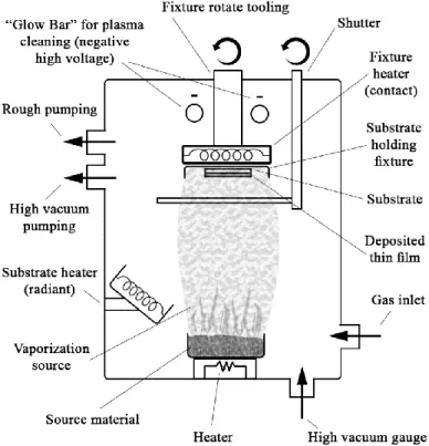
A vacuum evaporation method, consists in evaporating or subliming a heated source material in vacuum. The transport it is done by a vapor to a substrate located a distance away,
4
on line of sight, through gas molecules, condensing it as a solid thin film on the substrate. A large range of source materials, can be used with different reactivity and vapor pressures.
On vacuum evaporation system, there is some key elements, such as the fixture heater, the shutter and the glow bar, as can be seen on Fig. 1.1. The fixture heater, prevents that particles do not settle down on the substrate causing pin holes and allows movement resulting in uniform deposition over the substrate surface. The shutter, acts as a filter, protecting the substrate from volatile contaminant material that can come on vapor from the source material, as well as the direct exposure of radiant heat on the substrate. The deposition time can be accurately controled by opening and closing the shutter. The glow bar is responsible to maintain the substrate surface free of plasma [10][9].
Fig. 1.1 - Schematic of a vacuum evaporation system.
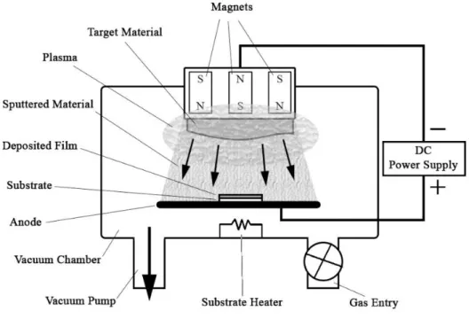
On sputtering method, a solid target material is bombarded with energetic ions, producing multiple collisions in the target materials surface, also known as sputter. This collisions will eject atoms from the surface into the gas, directly to the substrate, to form thin films that can vary from some nanometers to microns. The ions are produced by plasma that are generated
5
above the target material, resultant of the ionization of the gas. This atoms that are sputtered from target, are excited when they enter on plasma and emit photons.
Using different materials to produce devices will require several target materials. The number of ejected atoms from the surface per incident ion is known as sputter yield.
The deposition rate is dependent of several parameters such as the softness of the target, the distance between target and substrate, and also the energy applied which can vary from several to a few thousand Watts (W) depending on the target area [10][12][9][11].
The schematic of a sputtering system is shown in Fig. 1.2.
Fig. 1.2 - Schematic of a sputtering system.
The Ion Plating (IP), is also known as Ion-Assisted Deposition or Ionization-Assisted Deposition (IAD), Ionized Physical Vapor Deposition (IPVD or iPVD), and Energetic Condensation. This is an atomistic vacuum coating process where the depositing film on a substrate is bombarded continuously or periodically by energetic particles, normally ions, that can affect the growth and properties of the film.
In arc vaporization, a high current and low voltage is applied on an anode or cathode surface where a target material is placed, in a low pressure gaseous atmosphere, creating a vapor with plasma, ions and particles of a target material, carried to a substrate. All the process is
6
made in vacuum. Within arc vaporization, can be found the Cathodic Arc (CAV), the Anodic Arc (AAV), the Vacuum Arc (VAV) and the Plasma Duct Arc (PDAV) [10].
On CD, can be found the Chemical Vapor Deposition (CVD) and the Chemical Solution Deposition (CSD) among others.
The CVD, is a sequential process, where a reagent gas or a mixed selection of gases, also known as precursor gas, are flowing through a carrier gas, into a reactor chamber with one or more heated objects to be coated. Near the object surfaces occur the chemical reactions, resulting on a deposition of a solid thin film on those surfaces. Can be applied to do shaped pieces, with inside and outside features. Through distillation techniques, it is possible to achieve high disposition purity, where the impurities are removed from gaseous precursors [13][14][15].
On CSD, an aqueous solution is deposited on a solid or flexible substrate, occurring a reaction through a reactor. The solution involves a precursor liquid, a solvent, and can be added chemical modifiers to control the chemical reactivity.
The preparation of a liquid precursor, can be made with through several methods, such as sol-gel and auto-combustion, among others [16].
A sol-gel, is a process that transforms a solution on a substance that has solid elements permanently suspended in a liquid, also known as colloids suspension, forming in the end a chemical viscous gel. This process can be done at room temperature, minimizing the degradation of both the material itself and any entrapped species, resulting on a substance with high purity. High porous materials can be prepared in this way. The precursors solutions are often expensive, sensible with humidity, and need careful with ageing and drying, limiting his application on large scale production [17][18].
The auto-combustion, is also known as citrate precursor method, and is achieved with nitrates with citric acid, that react when heated, making a spontaneous combustion resulting on a ferrite sample. This method have the same properties as the mentioned sol-gel, with self-combustion properties. On self-self-combustion, there is only need a heat treatment at low temperatures to for solid films [19].
Can be found on CSD category, the Spin Coating Deposition (SCD), the Dip Coating Deposition (DCD), and the Inkjet Printing among others [20].
7
The SCD, is a method that deposits a solution on a substrate, mounted on a heated rotative platform which will spin till all the solution be thin on the surface of the substrate, and then occurs the evaporation of by-products.
On spin, there are two forces applied to balance the quality of the resulting coat, the spin-up and the spin-off. In the spin-spin-up, occur an acceleration where the solution flows radially outward, driven by a centrifugal force. On spin-off, the spinning remains at constant rate where the excess liquid flows into the perimeter and forms droplets on the surface of the substrate. Fig. 1.3 shows the SCD stages [21][22].
Fig. 1.3 - SCD stages: (a) material deposition on the surface of the substrate, (b) spin-up, (c) spin-off and (d) evaporation.
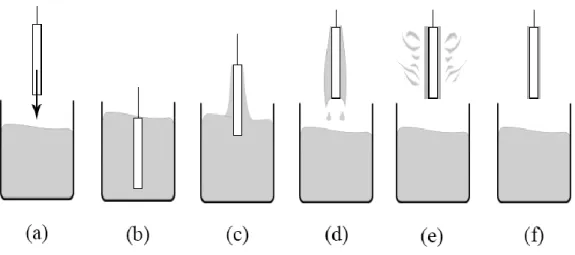
On DCD, the substrate is usually submerged vertically on a reservoir, with the precursor liquid, and a film is formed when the substrate is being removed at constant speed from the precursor. The substrate can be removed from the container, or the precursor can be drained from the reservoir. To evaporate solvents, a heated source is used, after the substrate bath. The formation of thin films in this process, is dependent of precursor viscous drag, gravitational forces, and surface tension. A schematic of DCD stages is shown on Fig. 1.4 [21][16].
8
Fig. 1.4 - DCD stages: (a)(b) bath of the substrate on the precursor, (c)(d) substrate removal of reservoir and precursor drain out and (e)(f) evaporation of solvents.
The method of inkjet printing can be divided in two categories, such as Drop on Demand (DOD) inkjet printing and Continuous Inkjet Printing (CIJ) [20].
The DOD technique, is a technology that ejects drops of ink on a nozzle when required, on a target sample, for example, plastic or paper. The DOD is a very popular type of fabrication to process organic materials. It is being adapted to process inorganic materials, but still limited on this type of materials. On this category, can be found several inkjet printing processes, such as the piezoelectric and thermal among others [20].
On piezoelectric process, the jet of the ink fluid is controlled by a voltage pulse, used to deform the crystals on the piezoelectric actuator, to allow the release of an ink drop from the nozzle, as can be seen in Fig. 1.5. This method can be found in domestic and industrial inkjet printers.
9
The thermal inkjet printing, use a print head that have a heat source, which evaporates temporarily some of the ink resulting in a bubble on the nozzle. The image data is send to the heat source. This process is described on the Fig. 1.6 [24].
Fig. 1.6 - Schematic of thermal inkjet printing [24].
On the CIJ, a stream of liquid is expelled from a reservoir, using a high pressure pump, and then flows out through a nozzle, resulting in a continuous stream of liquid. A piezoelectric actuator is used to produce a stream of small droplets, through acoustic waves focus on the nozzle. When the droplets fall out, an electromagnetic field is used to charge the ink according to the desired image.The stream of charged droplets can be electromagnetically deflected into a recycling system or allowed to hit directly the paper. The recycling system, is reserved for droplets that have been charged at a certain point. On Fig. 1.7 can been seen a CIJ schematic [20][24][25].
10
Fig. 1.7 - Schematic of a CIJ [24].
1.3. MATERIALS OF LAYERS
The ITFTs, are composed with four types of layers, the semiconductor, the gate dielectric insulator, contacts and the substrate. The semiconductor layer is a material that neither is conductor or insulator, composed by negative or positive types of materials.
On negative type (n-type) materials, electrons can flow out more naturally. On positive type (p-type) materials, electrons from nearby materials tend to flow into it [26].
Within ITFTs, there are several materials that have been used as layers.
Materials like Si and glass can be used as substrate but improvements has been done on the last few years to use also flexible and transparent substrates, such as plastic substrates, like Polyethersulfone (PES), Polyethylene Terephthalate (PET) and Polyethylene Naphthalate (PEN). On Si substrates, the gate can be present already on the substrate, if this layer be heavy doped.
As electrodes, it is used Indium Tin Oxide (ITO), Titanium (Ti), Molybdenum (Mo), Aluminum (Al) and Gold (Au).
Could be found as semiconductors, several p-types like, Zinc Tin Oxide (ZTO), Indium Zinc Oxide (IZO) and Gallium Indium Zinc Oxide (GIZO or IGZO).
11
On the dielectric insulator, it has been used, Silicon Dioxide (SiO2), Silicon Oxy Nitride (SiOxNy), Aluminium Oxide (Al2O3), Yttrium Oxide (Y2O3), Hafnium Oxide (HfO2), Zirconium Oxide (ZrO2), Titanium Dioxide (TiO2) [27][28][6][29][30][31].
1.4. DEVICE STRUCTURE
On TFTs category exists four types of physical structures.
There are the top and bottom gate structures, and both structures can be staggered or coplanar on TFTs. Issues with different fabrication methods and applications, lead to different structures.
In a top gate configuration, the gate and insulator are located on the top of the semiconductor. The bottom gate configuration, is referred as an inverted TFT, since it have the gate and insulator located beneath the semiconductor [32].
On coplanar configuration, the drain and source contacts, and the insulator are on the same side of the semiconductor. Between drain and source, there is a direct contact with the induced channel. Fig. 1.8 represents a coplanar configuration with bottom gate and top gate.
(a) (b)
Fig. 1.8 - Coplanar configuration with (a) bottom gate and (b) top gate [33].
In a staggered configuration, the drain and source contacts are on an opposite side of the semiconductor in comparison with the insulator. The drain and source are not in direct
12
connection with induced channel. It is used very large contact areas on this configuration. On Fig. 1.9 is shown a staggered configuration with bottom gate and top gate [32].
(a) (b)
Fig. 1.9 - Staggered configuration with (a) bottom gate and (b) top gate [33].
There are several important distances in the layers of TFTs structure. The distance L between drain and source is called channel length or region. The distance W is called channel width and represents the length of the device viewed from the lateral direction. The dielectric layer have a thickness known as tox. These distances are described on the staggered bottom gate TFT represented on Fig. 1.10 [1].
(a) (b)
13
1.5. OPERATION AND PARAMETERS
The principle of FET, derives from its own name from the essence of its physical operation. A field effect is created by a signal on gate terminal that is isolated from the rest of the device through a dielectric layer, creating a channel region on the semiconductor, between drain and source terminals, letting flow a second signal from drain terminal to source. The signal on gate terminal controls the flow of current between the drain and source terminals. The FET is also known as the unipolar transistor, since it only needs one polarity to work. This channel is formed by current that uses p-type or n-type materials as carriers. The channel region can be created by negative or positive signals on gate and source terminals, depending on what type of carrier is used [1].
The p-type and n-type semiconductors, can work at two operation modes, the Enhancement (E-device) or accumulation and at Depletion (D-device).
On the accumulation mode, there is no channel region constructed being developed only when a voltage is applied to the gate terminal. In these devices a certain minimum gate voltage (𝑣𝐺) is required to induce a conducting channel, called the threshold (𝑉𝑡ℎ) or turn on voltage. The enhancement name comes from the fact that the channel needs to be “enhanced” to cause conduction. This mode can be seen on Fig. 1.11 for a cross view of a staggered bottom gate TFT [34][35].
Fig. 1.11 - Cross view of accumulation mode on a staggered bottom gate TFT [36][1].
Traveling along the channel region, from source to drain, the voltage measured relative to the source, increases from zero to drain-to-source voltage (𝑣𝐷𝑆). Thus the voltage between
14
the gate and points along the channel decreases from gate-to-source voltage (𝑣𝐺𝑆) at the source end to 𝑣𝐺𝑆− 𝑣𝐷𝑆 at the drain end. Since the channel depth depends on 𝑣𝐺𝑆, the channel region assume a non-uniform shape as is represented on Fig. 1.11, being deepest at the source side and shallowest at the drain side. With the increase of 𝑣𝐷𝑆, the channel becomes more conic and the resistance increases as can be seen on Fig. 1.12 [1].
Fig. 1.12 - Illustration of the channel region states.
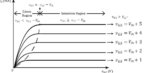
Thus the drain current (𝑖𝐷) increases, going from off-state (𝑖𝑜𝑓𝑓) to on-state (𝑖𝑜𝑛), entering on linear or triode region of operation till the voltage between gate and channel reduces at the drain to 𝑉𝑡ℎ = 𝑣𝐺− 𝑣𝐷𝑆 and the channel depth at the drain side decreases to almost zero, being called this switch of state, the pinched off channel. When 𝑖𝐷 is not rising significantly at the effect of 𝑣𝐷𝑆, the channel remains constant and the device enters on saturation or active region of operation. With 𝑖𝐷 = 0 for any 𝑣𝐷𝑆, there is no channel formed, being known as cut-off region. Fig. 1.13 shows a graphic 𝑖𝐷-𝑣𝐷𝑆, also known as I-V characteristics, representing the linear and saturation regions evolution when the tension at gate is rising [1][37][38].
15
Fig. 1.13 - Characteristics of the I-V characteristics of a p-type semiconductor with accumulation mode.
The linear region can be described through the equation (1.1),
2 2 1 ) ( GS th DS DS OX n D v V v v L W C i (1.1)
and the saturation region (1.2),
2 ) ( 2 1 th GS OX n D v V L W C i (1.2)
where this current is proportional to the ratio of the width and length channel, being known as aspect ratio. This ratio is created by the circuit designer to obtain the desired I-V characteristics. The 𝐶𝑂𝑋 is the capacitance per unit area of the parallel-plate capacitor formed by the gate terminal and the channel, with the dimension of 𝐹 𝑐𝑚⁄ 2, known as oxide capacitance and can be also represented as,
OX OX OX
t
16
where the 𝜀𝑂𝑋 is the permittivity of the dielectric layer, and the 𝑡𝑂𝑋 is the thickness described on last sub chapter.
With a constant 𝑣𝐷𝑆 and a rising 𝑣𝐺𝑆, can be measured the current 𝑖𝐷 response, to determine the 𝑉𝑡ℎ, as can be seen on Fig. 1.14, where this curve is also known as transfer function. A common practice to determinate the 𝑉𝑡ℎ is using the Extrapolation in the Linear Region (ELR) method. Choosing the maximum point of current, on the higher point of the maximum slope, with the beginning of the rising current of the lower point of the maximum slope and intercept the gate-voltage axis at 𝑖𝐷 = 0. This 𝑣𝐺𝑆 value for 𝑖𝐷 at zero is the 𝑉𝑡ℎ [38][39][40].
Fig. 1.14 - Characteristics of the transfer function curve of a p-type TFT with accumulation mode.
It is also possible to determine the electron mobility with the slope used on ELR method and equation (1.2), through the equation (1.4):
CoxW L slopeMAX n 2 (1.4)
17
The data of transfer functions can be also linearized to extract quantitative information. This can be done using a 𝑖𝐷1 (1+𝛾)⁄ vs 𝑣𝐺𝑆 representation, where the parameter 𝛾 represents the factor used in the linearization.
By other hand, there is the depletion mode, which devices could conduct to 𝑉𝑔 at zero voltage, being needed a 𝑉𝐺𝑆 to “deplete” the channel, to turn the device off. The depletion mode is also referred to as a buried channel, once current flow is not at the surface, like accumulation mode, but away from the surface in the bulk of the semiconductor [34][35].
Table 1.1 shows brief characteristics of these four different types of transistors.
Table 1.1 - Four different types of TFTs [35].
Gate Voltage
Device Type Normal State p-type n-type
Accumulation Mode OFF + 𝑉𝑔 turns on − 𝑉𝑔 turns on Depletion Mode ON − 𝑉𝑔 turns off + 𝑉𝑔 turns off
18
CHAPTER 2.
THERMAL STIMULATED
CURRENTS ON TFTS
This chapter provides a review of the thermal stimulated techniques used to characterize electronic traps in materials and devices. The basic equations are presented together with the relevant parameters and their physical meaning. This chapter also presents the basic procedures to perform the measurements and the limitations of the technique.
19
2.1. THERMAL STIMULATED CURRENTS
On TFTs, through Thermal Stimulation Current (TSC) measurements it is possible to confirm the presence of trapped charge carriers. These traps are filled when it is applied a voltage bias, where the temperature is such that the trapped currents cannot release through thermal energy.
The TSC measurement consists in raising the temperature linearly, releasing the trapped carriers. The released carries contribute to the excess current, measured as function of temperature during heating, is known as thermal stimulated current.
For a single trap level, a TSC curve has a maximum whose position in temperature depends on capture cross section, heating rate and trap depth. The cross section, is an area around a certain molecule in which can collide with near molecules. This maximum can be also determined varying the heating rates, the trap depth and the capture cross-section [41].
This measurement can only be done with insulated materials, because this detrapping currents are very small at pico (10−12) amperes. It is measured, normally with turned off or fully depleted TFTs. The configuration used with TSC experiments, is as a Metal-Insulator-Semiconductor (MIS) capacitor.
When TFTs are connected as capacitors to perform TSC experiments, often the bottom electrode is the entire substrate. When a filling bias is applied, it may charge the entire semiconductor which is larger than the transistor area. The charges in proximity of the TFT can diffuse to the contacts and the leads, where they are collected to be measured in the external circuit. The released charges during the TSC curve are extracted from an area larger than that between the TFT electrodes. This may lead to discrepancies between the total charge expected and the measure charge.
The experimental procedure starts with the trap filling at room temperature, where this filling bias are kept until the TFT is brought to low temperatures, low enough to ignore the detrapping. Then the configuration of the TFT must switch to be used as a capacitor, where the drain and source terminals are short, and a picoammeter measures the capacitor discharging current between the gate terminal and the drain and source terminals. After this, a temperature ramp is applied at a constant rate,
20 dt dT
(2.1)
up to high temperatures. The trapped carries are then released and collected by the grounded source and drain electrodes. The temperature where a current peak occurs is related to the energetic depth of the trap state, and the area under the peak is related of the trap density.
Fig. 2.1 shows TSC curves of an OTFT, where the curve recorded without trap filling is known as base line, to prove that the current is in reality a detrapping current.
Fig. 2.1 - Representation of TSC curves measured from an OTFT used as a MIS capacitor [42].
The integrated total charge can be determined through,
eN A Idt
Q t (2.2)
where the 𝑒 represents the electron charge, the 𝑁𝑡 is the density of filled traps and the 𝐴 is the surface area between the electrodes.
The extraction of the trap parameters from TSC measurements is not simple. The current temperature profile depends also on charge transport such as the charge carrier mobility and the occurrence of retrapping. To remove trap parameters can be applied several methods, such as the inicial rise time, the heating rate and the curve fitting.
21
The initial rise method assumes that the current in the initial part of the curve is exponentially dependent on temperature when the traps begin to leak. This method is typically used when the full TSC curve cannot be recorded or is distorted by other processes. Usually this method is less accurate than the other methods and only provides the trap depth.
To determine the trap depth 𝐸𝑇, from the relation between heating rate 𝛽, and the temperature of the maximum peak 𝑇𝑚, can be used as described by Blood and Orton,
B T m B T m m k E T k E T T ln ln 4 (2.3)
where 𝜎 is the capture cross section and γ is a parameter depending on the effective mass. The heating rate method consists in a series of TSC curves a different heating rates, where the 𝑇𝑚 can be determined. The activation energy of the trap can be obtained from 𝑇𝑚 with a linear plot of 𝑙𝑛 (𝑇𝑚2⁄ ) in function of 1 𝑇𝛽 ⁄ 𝑚. Then the slope yields a value for the activation energy.
The curve fitting method, assumes that monomolecular recombination of the charger carriers from a discrete set of traps with a single trapping level with a 𝐸𝑇 below the conduction band, with negligible retrapping. The current then follows,
off I Be Ae I 2 2 1 1 (2.4) in which, { v e n A t m e k vE B m B T 2 m B T T k E (2.5)
where 𝑛 represents the initial trap density of traps filled, τ is the average lifetime for a free carrier, µ is the electron mobility mentioned before and 𝑣 is the attempt to escape frequency. The TSC curves can be fitted with four parameters, 𝑇𝑚, 𝐴, 𝐸𝑇 and 𝑖𝑜𝑓𝑓. It have been noticed that at high temperatures, when a significant number of traps is emptied, the conductivity of the TFT channel is partially restored and the associated background current severely distorts the
22
measurements. For temperatures above the TSC peak the current cannot be treated only as a detrapping current and the analysis is usually not possible [42][43].
23
CHAPTER 3.
EXPERIMENTAL
This chapter is focused on the introduction of the equipment that was used, and how the devices are mounted and connected to the measuring instrumentation on experimental environment.
24
3.1. ASSEMBLY OF THE EQUIPMENT
To measure the current 𝑖𝐷, was used the Keithley 6487 current measurement connected to the source contact of the transistor on the target substrate. The currents across the device are typically below the micro-ampers range, and for this reason it is necessary to use pico-amperimeters. The voltage source used as 𝑣𝐷𝑆 was the Keithley 6487 that was connected on drain contact of the transistor. On the Keithley 487 was just used the voltage source as 𝑣𝐺𝑆, connected on gate contact. This configuration is applied to measure I-V characteristics and transfer functions of a TFT, as is represented on Fig. 3.1.
Fig. 3.1 - Schematic diagram showing the electrical connections on the TFT.
To measure a TFT as a capacitor, the Keithley 487 is disconnected from the chamber, and just the picoammeter from the Keithley 6487 is used, with the source and drain female contacts shorted, and then connected to the instrument as well as the gate contact, as is represented on Fig. 3.2. This configuration is used to measure TSCs on TFTs.
25
Fig. 3.2 - Schematic representation of a TFT connected as a capacitor to measure TSCs.
All the transistors were measured under a vacuum environment to avoid contamination such as water and oxygen on the surface, because there is no encapsulation on the devices. It was used two different vacuum chambers, a mere vacuum chamber and a cryostat.
The simple vacuum chamber was used only to perform measurements at room temperature. Where the TFT was simply placed inside of the chamber on a platform. All connections on the source, drain and gate terminals of the TFTs were made with adjustable metallic needles. A blue LED was mounted directly above the TFT inside of the chamber. The vacuum system used was only a Varian SD-201.
The cryostat was used to perform measurements as function of the temperature in a vacuum environment. It was used a configuration on the experimental environment, with the TFTs inside of the chamber, tied on a platform, and regulated to be at direct eye contact on the windows chamber. All connections on TFTs were made using a thin gold wire of 25µm in diameter glued to the source, drain and gate terminals with conductive silver. On the platform, it was used a plastic isolator to separate the substrate and the thermal sensor that was connected to the Oxford ITC. Inside the chamber were resistors that was connected also to the Oxford ITC.
Near the chamber was the Horiba Triax 320 spectrograph, with the output light len aligned with the chamber window, to expose the light directly on the substrate. The spectrograph light
26
was provided by the xenon lamp FL-1039 that was powered by a DC current source, the Eurosep Instruments Xenon DC 75-300.
The vacuum system, consists in an open system composed by the turbine Varian Turbo-V 70 helping the vacuum pump Turbo-Varian SD-201 to get a higher vacuum coefficient. The turbine was connected to the chamber. On the vacuum pump, there was an exhauster part to extract all the air from the system.
The current measurement and voltage source of the Keithley 6487 was connected to specific female connectors of the chambers. On the Keithley 487, just the voltage source was connected to the chambers, also on specific female connectors.
The instrumentation was all connected to a personal computer that controls the instruments through two types of interfaces, the GPIB and the RS232. The data was recorded in scripts that can be run in MATLAB TM software. All the data analysis and processing was made using MATLAB TM. The schematic of the equipment set is represented on the Fig. 3.3.
27
Fig. 3.3 - Schematic of the entire experimental set-up on the cryostat chamber.
3.2. SHORT DESCRIPTION OF THE INDIVIDUAL EQUIPMENT AND
SPECIFICATIONS
The experimental set was composed by several equipments, like a vacuum pump and turbine, a lighting device, a spectograph, a regulator and temperature gauge, two picoammeters and voltage sources, and a cryostat chamber.
The vaccum pump used, was a Varian SD-201 that works at 6,8 CFM (Cubic Feet per Minute), to achieve a high pumping stability, and can be seen on Fig. 3.4 (a) [44].
To achieve a higher pumping coefficient, have been added the Varian Turbo-V 70 vacuum turbine to the flow system. This turbine can pump at 75000 rpms at max. speed, and can be seen on Fig. 3.4 (b) [45].
28
When connected in series both pumps can evacuate the cryostat to a pressure of 10-6 Torr. This vacuum is important to prevent water condensation inside the cryostat when the TFT is cooled down to very low temperatures.
(a) (b)
Fig. 3.4 - Photograph of the (a) Varian SD-201 and the (b) Varian Turbo-V 70.
The lighting power supply used, was the Eurosep Instruments Xenon DC 75-300, represented on Fig. 3.5. This device can supply power to a xenon lamp at a maximum DC current of 10 A [46].
Fig. 3.5 - Photograph of Eurosep Instruments Xenon DC 75-300.
To modulate the light, it was used the Horiba Triax 320 spectrograph, as can be seen on Fig. 3.6 (a). This device comes also with a 450 W xenon lamp shown on Fig. 3.6 (b) [47].
29
(a) (b)
Fig. 3.6 - Photograph of the (a) Horiba Triax 320 spectrograph and the (b) FL-1039.
As regulator and temperature gauge, was used the Oxford Intelligent Temperature Controller (ITC), to measure the temperature in Kelvins (K). It uses as a temperature sensor a PT 100 (platinum sensor). This instrument is also capable to generate well-defined heating ramps through a resistor. This device is shown on Fig. 3.7.
Fig. 3.7 - Photograph of the Oxford Intelligent Temperature Controller.
One of the picoammeters and voltage sources used was the Keithley 6487, as can be seen on Fig. 3.8. This device have a picoammeter with a current resolution of 10 fA (10−15𝐴) and can measure from 20 fA to 20 mA. Can work at 1000 readings per second and have a storage buffer of 3000 points. The voltage source have a range between 200 µV to 505 V with a resolution of 0,2 mV, and also allows automated voltage sweeps for I-V characterization [48].
30
Fig. 3.8 - Photograph of the Keithley 6487.
The other picoammeter and voltage source was the Keithley 487, as is shown on Fig. 3.9. This model is similar with the previous one having the same current resolution. The current range its between 2 nA and 2 mA. Can read at 180 points per second and have a buffer with 512 points. The voltage source can operates at the same range and allowing a voltage sweep for I-V characteristics like the previous model but with a resolution of 1 mV [48][49].
Fig. 3.9 - Photograph of the Keithley 487.
The cryostat chamber used is shown in the Fig. 3.10. Composed inside with a substrate holder and is prepared to add temperature sensors and sources of heat. Outside have a cold finger to insert nitrogen liquid near the substrate holder to reduce temperature. The cryostat is also equipped with a sapphire window for optical experiments. It have also input and output female connectors, to connect all kind of devices.
31
32
CHAPTER 4.
ELECTRIC CARACTERIZATION OF
ZTO BASED TFTS
In this chapter the characteristics and the basic performance of the TFTs with urea and without urea are compared and discussed.
The ZTO based solution can be deposited by spin coating, or even by printing techniques. This opens very interesting way for the manufacturing of transistors and circuits in large areas on flexible substrates and by using low-cost processing methods.
33
4.1. CHARACTERISTICS AND PARAMETERS
The studied TFTs are made by several materials of layers. The semiconductor was made from ZTO, the dielectric insulator was SiO2 with a 𝐶𝑜𝑥 of 32 𝑛𝐹/𝑐𝑚2, the gate contact was made from a heavy doped Si to act as a conductor, the source and drain contacts were made from Al. Both gate and dielectric insulator are the substrate Si/SiO2. The structure of one transistor, as well as their material layers can be seen on illustration on Fig. 4.1.
Fig. 4.1 - Illustration of a SiO2+ZTO transistor.
The layout was composed by nine transistors with a common gate per substrate. Each transistor has a different dimension ratio of W/L. The configuration used was the staggered bottom gate. Fig. 4.2 represents a wafer with oxide TFTs.
Fig. 4.2 - Photograph of a wafer of nine SiO2+ZTO transistors with each ratio per transistor. The dimensions W and L are in micrometers.
34
Both wafers were processed with a SCD. The precursors solutions, Zinc (Zn) and Tin (Sn) was prepared individually on a bottle of glass with the solvent 2-Methoxyethanol, and blended for a day on an isolated environment to avoid evaporation of the used solvent. A day after of being resting, both precursors were mixed, and blended for an hour until we have the sol-gel precursor and then deposited through SCD on the Si/SiO2 substrate, resulting on a SiO2+ZTO without urea. To insert urea on the compound, it was added ammonium nitrate with the urea, being mixed with the rest of the compounds mentioned before, obtaining the auto-combustion precursor to be deposited through SCD. The drain and source contacts were deposited throughvacuum evaporation method.
4.2. CHARACTERIZATION OF TFTS WITH UREA
Several measurements were carried out on oxide based TFTs with urea. This is schematically represented in Fig. 3.1. In order to select the best ones, preliminary experiments were done in vacuum, without light and at room temperature. This means TFTs with no current leakage and good modulation. A typical transistor is the one labeled D5 with a W/L=14. Fig. 4.3 can be seen the I-V characteristics.
35
Fig. 4.3 - I-V characteristics of the oxide based TFT with urea labeled D5.
To know the threshold voltage of the transistor D5 it was taken also the transfer function, as can be seen on Fig. 4.4.
Through the ELR method mentioned on sub chapter 1.5, to determine the threshold voltage, we discover that the transistor have a 𝑉𝑡ℎ= 1,9 𝑉 using the dashed slope. It was used also to determine the electron mobility that is 0.76 𝑐𝑚2 𝑉−1𝑠−1. We also notice that the channel of these TFTs work at depletion mode as can be seen for voltages lower than zero on the gate.
36
Fig. 4.4 - Transfer function on linear region of the oxide based TFT with urea D5.
4.3. CHARACTERIZATION OF TFTS WITHOUT UREA
On oxide based TFTs without Urea, the same selection process have been applied in order to use the best transistor without current leakage, or less current leakage, and good modulation, and it has been chosen the labeled D9 W/L=60. Fig. 4.5 can be seen the I-V characteristics.
37
Fig. 4.5 - I-V characteristics of the oxide TFT without urea labeled D9.
To determine the threshold voltage it have been taken also the transfer function of the transistor, as can be shown on Fig. 4.6. We discover that the transistor have a 𝑉𝑡ℎ= 0.4 𝑉 and an electron mobility of 1.12𝑐𝑚2 𝑉−1𝑠−1. We also notice that the channel of these TFTs work at depletion mode as can be seen for some voltages less than zero on the gate.
38
Fig. 4.6 - Transfer function on linear region of the oxide TFT without urea D9.
4.4. DISCUSSION AND CONCLUSION
Comparing both characteristics it was observed that TFTs without urea have a lower threshold and a significant higher current approximately 2.0 A while the TFTs with urea can only reach a current 1 A. It was also noticed that TFTs without urea have a higher electron mobility of 1.12𝑐𝑚2 𝑉−1𝑠−1 while the TFTs with urea only have 0.76 𝑐𝑚2 𝑉−1𝑠−1.
This suggests that TFTs prepared with urea have a higher density of traps that degrades their performance.
39
CHAPTER 5.
STIMULATED CURRENTS ON
ZTO TFTS WITH UREA
This chapter is organized as follows, first the wavelength of light used to excite the TFT with urea is selected by studying the spectral dependence of the photo-generated current. The light-induced effects on the TFT characteristics are then presented and discussed. Thermal detrapping experiments together with temperature dependent experiments are used to get the energetic depth of the light-induced state. It is proposed that these states are ionized oxygen vacancies. Finally, it is discussed how these finding may be explored to fabricate a Charge-Coupled Device (CCD).
40
5.1. TRAP FILLING WITH LIGHT
The photo-response of TFT with urea as function of the wavelength is shown in Fig. 5.1. In the wavelength range of 450-550 nm the photo-generated current is low and relatively flat with wavelength. In the infrared region (>560 nm), the current rises because of the heat generated by the infrared light. The photo-generated current rises as the energy of the light increases and for wavelength above 400 nm reaches a plateau. The maximum value is at 400 nm (E=3.5 eV) which is in line with the value of 3.8 eV reported in the literature for the band-gap of ZTO, by Yinzhu Jiang [50].
Fig. 5.1 - Photo-generated current on ZTO TFT with urea as function of the wavelength.
Light with band-gap energy (3.01 eV) was used to photo-generate carriers and induce the electronic states. Prior to the TSC experiments, the TFT was electrically characterized.
On Fig. 5.2 (a) shows the transfer curves measured in the linear region (VDS = 0.25 V)
before and after illumination. There is dramatic increase in the current. Since the transfer curves were recorded in the linear regions it is expected that the transfer curves should be linear. The fact that the transfer curves are curved over the entire voltage makes difficult to extract quantitative information. Namely, it is difficult to estimate if there is a change in mobility and what the real changes in the threshold voltage are.
41
In order to extract quantitative information we first have to linearize the curves. This is done in Fig. 5.2 (b). To linearize the curves we use the parameter as described in chapter 1.5. The curves in Fig. 5.2 (a) were linearized using =1. The IDS is then plotted as IDS1/2 vs VGS in
Fig. 5.2 (b). After this linearization process, both transfer curves follow a straight line. The black dashed line in Fig. 5.2 (b) is a guide to the eye to show how much the transfer curve (ii) deviates from the original slope (i).
The light increases the current but also changes the field-effect mobility. In overall terms there is a change in the charge transport mechanisms. The electron mobility is calculated from the black dashed lines in Fig. 5.2 (a) where it rises from 0.76 𝑐𝑚2 𝑉−1𝑠−1 to 4.25 𝑐𝑚2 𝑉−1𝑠−1 upon light. This effect can only be explained if the light creates dopant states.
(a) (b)
Fig. 5.2 - Light induced changes on the linear transfer curves. (i) The transfer curves before and (ii) after 1000 seconds of light exposure. Both transfer curves were measured in the linear
region (VDS = 0.25 V).
5.2. THERMAL STIMULATED CURRENTS
The TSC experiments were performed as described on sub chapter 2.1. The states are filled with light at room temperature and the TFT is cooled down to 160-200 K while the TFTs
42
is kept under illumination. Then the illumination was switched off and the TFT is connected as a capacitor. The current between the gate terminal and the short-circuited drain and source terminals was measured. The short-circuit current was measured as the TFT was warm-up to 360 K. A well-defined heating ramp with 1.08 K/min was used as shown in Fig. 5.3.
Fig. 5.3 - Heating ramp used during the thermal detrapping currents. The heating rate is 1.08 K/min.
First a TSC curve was recorded without previous light excitation. This curve is shown in Fig. 5.4. The current is very low (I <5 pico-amps) and has a flat behaviour with temperature. This is the leakage current through the gate dielectric.
When the TSC is recorded after light exposure, the temperature dependence is no longer flat but instead two clearly peaks are observed, one negative and other positive. At low temperatures there is already a current of about -300 pA that keeps increasing with temperature until 260 K. Then the temperature dependence changes and the current will start to increase to positive values. At around 310-320 K the current changes polarity and becomes positive. It will reach a positive peak of 450 pA at the temperature of 350 K. The shape of the curve suggests that there are two depolarization currents of opposite polarity, one for low temperatures that peaks at around 260 K and another that peaks at 350 K. The negative peak corresponds to the
43
release of minority carriers (holes) while the positive peak corresponds to the release of electrons (majority type of carriers).
Fig. 5.4 - TSC: (i) curve recorded without light filling (base line) and (ii) curve recorded after light filling at room temperature for 1000 seconds.
The sign of the carriers released can be determined by the configuration of the experimental set-used. The connections used when the TFT is connected as a capacitor is schematically represented in Fig. 3.2. If the current is negative then this must correspond to the flow of electrons from the TFT channel to the source and drain terminal.
The effect of the applied bias on the shape of the current was also tested. The negative peak caused by the release of holes is strongly affected by the applied bias. It moves to higher temperatures when an accumulation channel is built by the application of a positive gate bias.
44
Fig. 5.5 - The effect of applying gate bias on the shape of the TSC curve: (i) curve recorded with gate bias of 0 V and (ii) curve recorded with a gate bias of 2 V.
As described in previous section, one of the procedures to extract the trap energetic depth of the defect responsible for this TSC current, is to perform several TSC curves with different heating rates. The peak position in temperature should move to higher temperatures has the heating rate increases. However, the peak is already in the border of our temperature observation window. Our upper temperature range is 360 K. Therefore, this method is not very practical. Furthermore, the shift of the peak with temperature is minimum. This suggest that the process that generates the TSC curve may not be totally controlled by a thermal detrapping process. As discussed on sub chapter 2.1, when the peaks in the TSC curves are not easily measured or they do not shift with temperature, can be used the initial rise method.
The initial rise method is valid for all types of recombination kinetics and assumes that the current in the initial part of the curve, when the traps begin to empty, is exponentially dependent on temperature. This method is often used when the full TSC curve cannot be recorded or is distorted by other processes. The method only provides the trap depth and is usually less accurate than the other models. The initial TSC curves in Fig. 5.4 and Fig. 5.5
45
follows a single exponential behaviour with an activation energy of 0.14 eV, as shown in Fig. 5.6.
Fig. 5.6 - Semilog-plot of the exponential rise in current observed in Fig. 5.4. The temperature range used is 260-350 K. The fitting to the curve provides an activation energy of 0.14 eV.
To gain insight into the possible mechanism that can be involved in this activation energy of 0.14 eV. The temperature dependence of the TFT current in the linear region was also measured before and after light excitation. The results are shown in Fig. 5.7. When the TFT is not excited with light, the bulk current (Vg = 0 V and IDS = 0.25 V) shows an activation energy
46
Fig. 5.7 - Temperature dependence of the transistor current measured in the linear region (VG = 0 V and VDS=0.25 V): (i) before light illumination and (ii) after light illumination.
In Fig. 5.7 it is also possible to see that above 300 K the current starts to decrease with temperature. This behaviour suggests that the dopant states responsible for the carrier transport become inactive, or alternatively some carriers get retrapped. The possible mechanism for this decrease in current with temperature will be discussed later.
5.3. DISCUSSION
The results presented above shown that the TFT can be programmed into a high conductive state. This high conductive state is programmed by exposing the band-gap of the ZTO with urea to light. After light exposure the TFT shows a high current and also a different charge transport. The field effect mobility increases 0.76 𝑐𝑚2 𝑉−1𝑠−1 to 4.25 𝑐𝑚2 𝑉−1𝑠−1, the activation energy for transport decreases from 0.22 eV to 0.14 eV. When the TFT is left in the dark at room temperature this high conductive state decays in a time scale of days to the original state. This long-lived decay is thermal activated and can be relatively frozen at low temperatures (T<260 K). This allows us to perform temperature dependent experiments and inspect for the
![Fig. 1.3 shows the SCD stages [21][22].](https://thumb-eu.123doks.com/thumbv2/123dok_br/18938342.939325/29.918.172.764.367.539/fig-shows-scd-stages.webp)
![Fig. 1.8 - Coplanar configuration with (a) bottom gate and (b) top gate [33].](https://thumb-eu.123doks.com/thumbv2/123dok_br/18938342.939325/33.918.149.797.666.921/fig-coplanar-configuration-gate-b-gate.webp)
![Fig. 1.9 - Staggered configuration with (a) bottom gate and (b) top gate [33].](https://thumb-eu.123doks.com/thumbv2/123dok_br/18938342.939325/34.918.142.799.222.486/fig-staggered-configuration-gate-b-gate.webp)
![Fig. 1.11 - Cross view of accumulation mode on a staggered bottom gate TFT [36][1].](https://thumb-eu.123doks.com/thumbv2/123dok_br/18938342.939325/35.918.226.728.697.877/fig-cross-view-accumulation-mode-staggered-gate-tft.webp)