Abstract— In this paper, design of dual-band equal-split Wilkinson power divider (WPD) with two and three transmission line (TL) sections is tackled from the perspective of a new simplified mathematical approach as compared to the previously presented work. It is mathematically proven and experimentally verified that only even-mode circuit analysis suffices for outlining the design guidelines for such WPDs which greatly reduces the mathematical complexity. Owing to the cascaded nature of the TL sections and using even-mode analysis, firstly, design equations and design graph are drawn for the two TL sections WPD. The technique is then extended to the design of a three TL sections WPD with simplifications in the circuit, rendering the approach much simpler and mathematically less rigorous (as compared to the previous work). The comparisons of the proposed and previous design approach are drawn. To prove the efficacy of the presented simplified design approach, a two TL sections and a three TL sections WPD are designed at 1GHz and 2.4GHz and fabricated. The measured S-parameters show good conformance with the simulated results indicating practical viability of the presented simplified approach. For instance the insertion loss in the two and three TL section is better than 3.2dB. The return loss and isolation between the ports in two TL sections WPD come out to be better than 28dB and 29dB, and in three TL sections is better than 30dB and 29dB respectively at the two design frequencies.
Index Terms— Dual-band, even-mode analysis, transmission line sections, Wilkinson power divider.
I. INTRODUCTION
Wilkinson Power divider (WPD) is one of the basic building blocks of most RF front-ends (RFFE)
owing to its equal/unequal power division and/or combination capability. With the advent of
multi-band transceiver systems, research focus has been shifted towards design of multi-multi-band WPDs,
digressing from the well-established design guidelines of conventional single frequency band WPD
[1]. For example, for dual-band operations (such as, but not limited to, GSM and PCS for cellular
phones), many techniques have been proposed for dual-band WPD design encompassing two
Transmission lines (TL) sections equal split [2-7], rat-race couplers [8], three TL sections equal-split
[9], unequal division [10-11] and meta-material based implementation of WPD [12-13]. Tri and
quad-A New Simplified quad-Approach for Design of
Dual-Band Wilkinson Power Divider with
Two and Three Transmission Line Sections
Using Only Even-Mode Analysis
Zafar Bedar Khan, Zhao Huiling, Zhang Yiminband WPDs are proposed in [14-15]. A two TL sections WPD with length equal to one third of the
design wavelength was proposed in [2]. The proposed approach, however, was limited to design at the
fundamental frequency and its first harmonic only. Addressing this limitation in [3], the author
presented closed form equations after extensive mathematics for design of dual-band WPD at any two
arbitrary frequencies. A two TL sections equal split WPD, proposed in [3] is shown in Fig. 1(a).
Nevertheless in [3] there was a room for improvements in the return loss and port isolation due to
poor response. Subsequently, in order to improve S-parameters response like insertion loss, return loss
and ports isolation (S21/S31, S11/S22/S33, and S23 respectively), RLC component were used in
[4-7]. Clearly for formulation of generic design guidelines over a wide frequency band, LC components
response may vary with the change in frequency and may additionally have increasing parasitic
effects as the frequency goes higher. One such attempt avoiding the use of LC components was
reported in [9] where a three TL sections equal division WPD operating at two arbitrary frequencies
was proposed. The design used only a resistor and a third transmission line section to improve upon
the return loss and isolation between the output ports as compared to [3] over a wide range of
frequency. This has an advantage in terms of repeatability and easy fabrication when it comes to the
micro-strip implementation. However, the method presented in [9] is mathematically extensive and
complex owing to formulation of four unknown parameters of the proposed circuit namely Z1, Z2, Z3
and R as shown in Fig. 3(a). These unknowns were found out by solving four non-linear
transcendental equations derived from the even and odd mode analysis after rigorous mathematical
derivations.
In this paper, generic design guidelines for two and three TL sections equal-split WPD for a wide
range of frequencies are presented based on a simplified mathematical approach for analysis of the
circuit parameters. The analysis throughout is based on the network theory and even-mode analysis
only, owing to the cascaded transmission line sections and symmetric nature of equal split WPD
structure respectively. Firstly, in order to build up the concept and extend it further, the simpler circuit
shown in Fig. 1(a), also presented in [3], is re-analyzed using the network theory (unlike [3]) and the
unknown parameters of the circuit are found out through even-mode analysis only.
Generic design graph for a wide range of frequency ratio (m = f2/ f1 where f1& f2 are two arbitrary
frequencies) is presented for two TL sections WPD. The idea is then extended to the design of three
TL sections WPD as shown in Fig. 3(a) (presented in [9]) with proposed simplifications. With
introduction of proposed simplifications in the three TL sections structure of Fig. 3(a) [9], it is shown
that the complexity of the analysis for determination of the unknown parameters of the circuit is
reduced to half with a fairly comparable operational response of all S-parameters. Experimental
verification of the design work based on the proposed simplified design guidelines comes from the
results of manufactured dual-band with equal split two and three TL sections WPDs. The operating
frequencies are 1GHz and 2.4GHz (with frequency ratio m = f2/ f1=2.4, where f1 is assumed to be less
range of the frequency ratio. The trade-offs of the proposed simplifications as compared to [9] are
discussed.
II. PROPOSED ANALYSIS
A. Two TL Sections WPD
Equal split two TL sections WPD shown in Fig. 1(a) is re-analyzed to formulate a general guideline
for design over a wide range of frequency ratio (m). The main advantage of the presented analysis is
that the derived non-linear equations are a function of m (through electrical length θ which in turn is a
function of m), unlike [3] in which the rigorous mathematical equations are function of the frequency
which, if changed, warrants the calculations again. Following mathematical derivations were extended
in the next sub-section to a three TL sections WPD design with proposed simplifications which
improves the performance of the WPD with two TL sections.
(a) (b)
Fig. 1. WPD with two TL sections (a) structure proposed in [3] and (b) bisected (half) circuit for even mode analysis.
i. Even Mode Analysis For Dual Band Operation
Due to symmetry of the circuit shown in Fig. 1(a), it can be bisected with input impedance equal to
2Z0 for even mode analysis as shown in Fig. 1(b). Treating the circuit in Fig. 1(b) as a cascaded
network of two TLs with unknown impedance of Z1 and Z2 (normalized impedances of z1 and z2
respectively), the ABCD parameters can be given as follows
1 2
1 2
cos jz sin cos jz sin A B jsin jsin cos cos C D z z
(1) So that 2 2 1 2 z sin A cos z
(2)
1 2
Bjcos sin (z z ) (3)
1 2
1 1
C jcos sin
z z
(4)
2 2 2 1 z sin D cos z
(5)
In order to ensure effective operation of the WPD at two arbitrary frequencies of f1 and f2 = mf1
(where m is the frequency ratio), the input impedance must be matched to the output impedance. As
0
in 0
0 B AZ
Z 2Z
D CZ
(6) Putting values of the A, B, C and D from (2)-(5) in (6) , simplifying and separating the real and imaginary parts, following two non-linear equations can be derived:
2 2 2
1 2 1 2
z z (z 2z ) tan 0 (7)
1 2 1 2 1 2
2(z z ) z z (z z )0 (8)
Here we have two nonlinear equations with two unknowns. No further analysis is required indicating
that even-mode analysis is enough which reduces the mathematical complexity. It is worth
mentioning here the very fact that taking equal division, only resistor as isolation element and system
characteristic impedance of Z0= 50 Ω into consideration, makes it possible to select R=100 Ω based
on extensive analysis [1, 4-7] for effective matching and sufficient isolation between the input and
output ports thus avoiding the odd-mode analysis. However for LC as isolation elements [4-5, 7]
and/or unequal division [9, 10] and/or more than one resistor as isolation element [11-12], as design
specifications, odd-mode analysis cannot be avoided.
Equations (7)-(8) can be simultaneously solved for different electrical lengths (θ). Note that the
electric length θ can be converted to physical length l by the relation θ=βl, where β is the wave
number. The physical length (l) formula is given in (9) [3] and at the lower design frequency (f1) the
electrical length (θ) which satisfies (7) and (8) is obtained from (10).
1 2
n
f1 f2
l l
(9)
f 1 n
1 m
(10)
Where n is a constant and its value is kept at 1 for smaller size, and m is the frequency ratio. The
physical lengths of the TL sections are kept equal [2-3].
Since electrical length (θ) is now known, the two non-linear equations (7) and (8) are
simultaneously solved for the unknowns z1 and z2. Fig. 2 presents a design graph in which the
normalized impedances z1 and z2 are plotted against a wide range of frequency ratio (m= f2/f1) on the
x-axis.
Contrary to [3], Fig. 2 shows a design graph for two TL section equal split WPD over a wide range of
frequency ratio (m) from 1.8 to 5. It is evident here that it is very easy to design and manufacture a
two TL sections equal split WPD with the proposed general design guideline.
B. Three TL Sections WPD
The complex and mathematically rigorous approach presented in [9] for determination of the
unknown parameters of the circuit shown in Fig. 3(a) can be greatly simplified.
Here, the proposed methodology in the previous sub-section is extended to the design of three TL
sections WPD with proposed simplifications in the circuit shown in Fig. 3(a).
(a) (b)
(c)
Fig. 3. WPD comprising of three section TL structure (a) Structure in [9] (b) Structure with proposed simplifications and (c) Bisected circuit for even mode analysis.
i. Proposed Simplification
The complexity of analysis in Fig. 3(a) owes itself to the variable impedances of the additional TL
section 3 and isolation resistor. It is proposed and proven here that for all practical purposes, the third
TL section in such kind of three TL sections equal split WPD design as shown in Fig. 3(a), can always
be treated as a 50Ω extension TL to increase the isolation between the output ports (ports 2&3) and
the return loss. In addition, for similar reasoning presented in section IIA, since the design under
consideration has equal-split power ratio and system characteristic impedance of Z0 = 50 Ω, no LC
components and only one isolation resistor (R), the value of R can be fixed to the conventional value
of 100 Ω [1, 4-7] without compromising the performance of the dual-band WPD. With the proposed
simplifications as shown in Fig. 3(b), the number of unknowns in the circuit is reduced to two, namely
Z1 and Z2, as compared to four in Fig. 3(a). It implies that the complexity can be brought down to half
as compared to [9] since the number of non-linear equations to be solved now can be reduced to two
instead of four. The two equations can be obtained by even mode analysis only, based on half circuit
in Fig. 3(c).
ii. Even mode analysis for dual-band operation
There is no current flow in the symmetric plane of the circuit shown in Fig. 3(b) due to application
was bisected at the middle as shown in Fig. 3(c).
With input impedance as 2Z0 at port 1 and treating the circuit in Fig. 3(c) as cascaded network of
two TLs and a third shunt TL with impedances of Z1, Z2 and 50 (normalized impedances of z1, z2 and
1) respectively, the ABCD parameters can be derived. Mathematically,
1 2
1 2
cos jz sin cos jz sin
A B 1 0
jsin jsin
cos cos
C D jtan 1
z z (11) So that 2
2 1 2
1 2
2 z sin
A cos (z z ) sin
z
(12)
1 2
Bj(z z ) cos sin (13) 2
2
1 2 1
jz sin tan
1 1
C j 1 cos sin
z z z
(14)
2 2 2 1 z sin D cos z
(15)
The input impedance of the circuit in Fig. 3(c) can be expressed as
0 in 0 0 B AZ Z 2Z D CZ
(16) Putting values of the A, B, C and D from (12)-(15) in (16) simplifying and separating the real and imaginary parts, following two non-linear equations can be derived:
2 2 2 2 2
2 1 1 2 1 2 1 2
(2z z z z z z ) tan z z 0 (17)
2 2 2 2
2 1 1 2 2 1 2 1 2
2(z z z z z tan ) z z z z 0 (18)
Similar to section IIA, at this point there are two equations with two unknowns. The analysis is
complete and no further computation is required for formulation of unknown parameters thus
circumventing the odd-mode analysis. Contrary to [9], the mathematical complexity has been greatly
reduced. Equations (17) and (18) are solved simultaneously with electrical length (θ) given in (10) to
obtain the unknowns z1 and z2.
Comparison of the normalized impedances varying with wide range of frequency ratio (m= f2/f1)
calculated through the proposed simplified method and [9] is illustrated in Fig. 4. It is evident here
that by the introduction of the proposed simplifications, the difference between the unknown
parameters is not much as compared to [9]. For example, it is clearly seen in Fig. 4 that the maximum
difference between the normalized impedance values of z1 and z2 is less than 9% and 3% respectively.
Whereas for m=2.3 to m=5, the maximum difference between the normalized impedance values of z3
and r is less than 15% and 20% respectively. The proposed design guidelines are also valid for a wide
range of frequency ratio (m) i.e. from 2 to 5. An additional advantage is that it replaces the resistor
with non- standard values in [9] with a conventional and standard value of 100 Ω which is easy to find
Fig. 4. Comparison of normalized impedances vs. frequency ratio (m) formulated through proposed work and [9].
C. Comparison of Proposed Technique with Referenced Work
Table I gives the comparison of the parameters calculated through the proposed method (Fig. 2 &
4) with other referenced works having similar equal split WPD structure with two and three TL
sections. It is clear from the Table I that following the proposed simplified technique presented in
section IIA & B, the difference between the calculated unknown parameters is very less thus
indicating the usefulness of the proposed analysis.
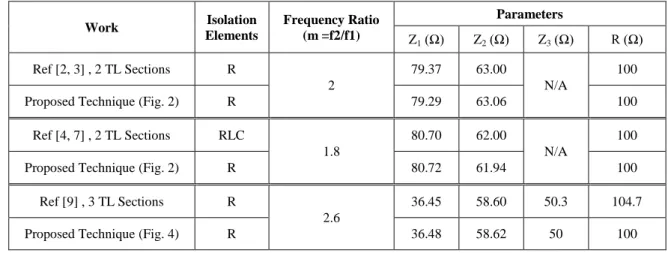
TABLE I:COMPARISON OF THE CIRCUIT PARAMETER VALUES OBTAINED THROUGH ANALYSIS OF SIMILAR TWO AND THREE TL
SECTIONS EQUAL SPLIT WPD PRESENTED IN DIFFERENT REFERENCES WITH THE PROPOSED TECHNIQUE
Work Isolation Elements
Frequency Ratio (m =f2/f1)
Parameters
Z1(Ω) Z2(Ω) Z3(Ω) R (Ω)
Ref [2, 3] , 2 TL Sections R
2
79.37 63.00
N/A
100
Proposed Technique (Fig. 2) R 79.29 63.06 100
Ref [4, 7] , 2 TL Sections RLC
1.8
80.70 62.00
N/A
100
Proposed Technique (Fig. 2) R 80.72 61.94 100
Ref [9] , 3 TL Sections R
2.6
36.45 58.60 50.3 104.7
Proposed Technique (Fig. 4) R 36.48 58.62 50 100
III. EXPERIMENTAL DEMONSTRATION OF THE PROPOSED TECHNIQUE
The proposed design guidelines in sections IIA & B for two and three TL sections equal split WPD
respectively are shown to be conveniently utilized for design of both types of dual-band equal split
WPD with m= 2.4, operating at f1 = 1GHz and f2 = 2.4GHz (note that m=3, is a special case where the
WPD designed through proposed technique can be simply replaced by a conventional λ/4 transformer
which has a property of operating at frequency f0 and its first odd harmonics 3*f0 [4]). Especially in
the design of three TL sections WPD, it is practically shown that there is no compromise on the
operational parameters (e.g. isolation between port 2 & 3 and return loss) while using the proposed
technique as compared to [9]. Based on design graphs of Fig. 2 and Fig. 4, the values of the circuit
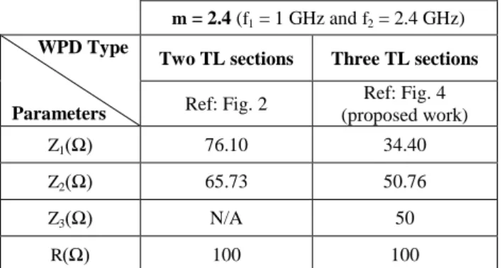
TABLE II:SUMMARY OF THE IMPEDANCE VALUES (AFTER MULTIPLYING WITH CHARACTERISTIC IMPEDANCE OF 50Ω) FOR TWO
AND THREE TL SECTIONS WPD
m = 2.4 (f1 = 1 GHz and f2 = 2.4 GHz)
WPD Type
Parameters
Two TL sections Three TL sections
Ref: Fig. 2 Ref: Fig. 4
(proposed work)
Z1(Ω) 76.10 34.40
Z2(Ω) 65.73 50.76
Z3(Ω) N/A 50
R(Ω) 100 100
The electrical length is, θ=530 when m=2.4. ADS software was used for all simulation and layout
work. Subsequently, the two circuits were fabricated on a substrate with dielectric constant of 2.2 and
thickness of 0.8mm. The fabrication of the PCBs was carried out on a Milling PCB prototype machine
with precision, repeatability tolerance and mechanical resolution of ± 20µm, ±5µm and ±0.8µm
respectively. The TL widths and lengths corresponding to the impedances mentioned in Table II were
calculated accordingly. Z0is taken to be 50Ω as mentioned earlier.
Fig. 5 shows the photographs of the fabricated dual-band equal split WPD with two and three TL
sections. As stated earlier, the physical lengths of the TL sections were kept equal [3]. The size of the
designed two TL sections WPD is 7 cm x 4.5 cm which is comparable to the two examples presented
in [4] whose sizes are 6.4 cm x 3.4 cm and 7.3 cm x 3.8 cm respectively. The exact size of three TL
section WPD in [9] is not given however the designed three TL sections WPD is 10 cm x 3.8 cm in
dimensions.
(a) (b)
Fig. 5.Fabricated dual-band equal split WPD operating at frequencies of 1GHz and 2.4GHz (frequency ratio m=2.4) (a) with two TL sections and (b) with three TL sections.
IV. MEASUREMENT RESULTS AND DISCUSSIONS
The measurements were performed on Agilent’s Phase Network Analyzer (PNA) model no. E8363B.
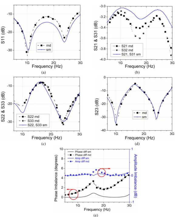
A. Two TL Sections WPD
A good agreement between the simulated and measured results can be noticed in Fig. 6 (a-e)
confirming the authenticity of the design guidelines given in Fig. 2 for two TL sections WPD. From
(a) (b)
(c) (d)
(e)
Fig. 6. Comparison of simulated and measured response of two TL sections WPD. (md = measured, sm = simulated)
Frequency response of (a) return loss at port 1 (S11) (b) insertion losses (S21 & S31) (c) return losses (S22 & S33) (d) output port isolation (S23) and (e) Phase imbalance (< S21- < S31)and Amplitude imbalance (|S21|-|S31|) at the two output ports.
and 2.4GHz respectively showing good impedance matching at port 1 with a maximum error of less
than 9% between the simulated and measured results.
Symmetry of the presented two TL section WPD can be inferred from almost overlapping measured
responses of S21 & S31 (with mutual difference of less than 2% as in Fig. 6(b)) and S22 & S33 (Fig.
6(c)) at the design frequencies. Output port isolation is yet another important parameter which is
shown in Fig. 6(d). Good isolation of S23=35dB and 30dB is observed at both operating frequencies
As expected the amplitude difference between the transmitted signal at port 2 and 3 (|S21|-|S31|) is
close to zero at the two design frequencies. Whereas the phase difference is about 1.50 and 20 at 1
GHz and 2.4 GHz respectively, being reasonably acceptable.
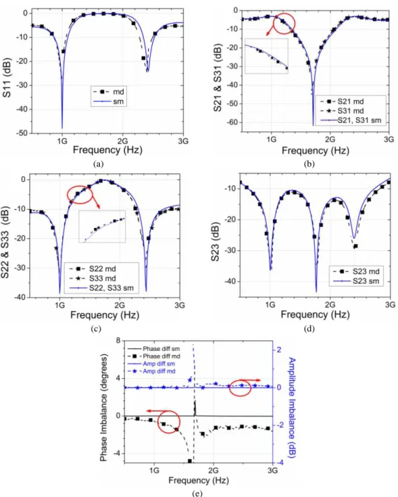
B. Three TL Sections WPD
Validity of the simplified design guidelines of Fig. 4 is established through conformance of the
simulated and measured S-parameters response presented in Fig. 7(a-e).
(a) (b)
(c) (d)
(e)
Fig. 7. Comparison of simulated and measured response of three TL section WPD. (md = measured, sm = simulated)
Frequency response of (a) return loss at port 1 (S11) (b) insertion losses (S21 & S31) (c) return losses (S22 & S33) (d) output port isolation (S23) and (e) Phase imbalance (< S21- < S31) and Amplitude imbalance (|S21|-|S31|) at the two output ports.
Good impedance match at port 1 is shown in Fig. 7(a) where the S11= 31dB at 1GHz (although the
division of signal is depicted in Fig. 7(b) with insertion loss S21 and S31 equal to 3.06 dB and 3.12
dB at the two design frequencies respectively. Return loss at port 2 & 3 (S22 and S33) is shown to be
30dB at both design frequencies in Fig. 7(c). Here also, the symmetry of the three TL sections WPD
circuit is evident from Fig. 7(b & c) due to the overlapping response of the insertion loss and return
loss at output port 2 & 3 respectively (shown in the inset graphs). Fig. 7(d) depicts the output port
isolation (S23), which comes out to be 36dB and 29dB at 1GHz and 2.4GHz respectively closely
following the simulated results. The proposed WPD has good response for a fractional BW of 20%
and 8% at 1GHz and 2.4GHz respectively. Last but not the least Fig. 7(e) shows the phase and
amplitude imbalance of the output signal at port 2 and 3 for 3TL sections WPD. The measured phase
and amplitude imbalance is -0.650, 0dB and -1.20, 0.1dB at 1GHz and2.4 GHz respectively.
From the comparison of Fig. 6 & 7, it can be drawn that in general the S-parameter response of the
dual-band WPD is better in the three TL sections design as claimed in [9]. Although two TL sections
design works well at the design frequencies, S-parameters response, especially the output port
isolation (S23) is improved in the three TL sections design.
V. CONCLUSION
Generalized design guidelines are presented for two and three TL sections equal split WPDs based on
a new simplified, mathematically much less rigorous approach which only requires even-mode circuit
analysis for evaluation of unknown impedances. For two TL sections WPD, treating the circuit as
cascaded network the unknown impedances are found out by even-mode analysis. The mathematical
approach is different than [3] through which, for equal split ratio, the values of impedances of the TLs
are formulated over a wide range of frequency ratio. The established technique is conveniently
extended to three TL sections WPD design where simplifications were introduced in the circuit
presented in [9], greatly reducing the mathematical complexity (to half) as compared to [9] without
compromising the performance of the WPD. It was established mathematically and was proven
experimentally that in such kind of WPD, the third section of the TL can always be replaced with 50Ω
impedance and the isolation resistor’s value can be 100Ω as in conventional WPD design. With these
simplifications, even mode analysis sufficed to find out the unknown parameters. Here too, the design
guidelines covered a wide range of frequency ratio. Dual-band equal spilt WPDs with two and three
TL sections operating at 1GHz and 2.4GHz were designed and fabricated based on the presented
guidelines respectively. The measured response showed very good conformance with the simulated
results with excellent performance parameters. The presented approach can serve as generic, much
simpler guidelines for design of such dual-band equal split two and three TL sections WPDs.
REFERENCES
[1] Pozar, D. M., Microwave Engineering, second edition, Wiley, New York, 1998.
[2] Chow, Y. L. and Wan, K. L., “A transformer of one-third wavelength in two sections-for a frequency and its first
harmonic,” IEEE Microw. Wireless Compon. Lett., Vol. 12, No. 1, 22–23, Jan. 2002.
[3] Monzon, C., “A small dual-frequency transformer in two sections,” IEEE Trans. Microw. Theory Tech., Vol. 51, No. 4,
[4] Wu, L., Sun, Z., Yilmaz, H., and Berroth, M., “A dual-frequency Wilkinson power divider,” IEEE Trans. Microw. Theory Tech., Vol. 54, No. 1, 278-284, Jan. 2006.
[5] Kawai, T., Nakashima, Y., Kokubo, Y., and Ohta, I., “Dual-band Wilkinson power dividers using a series RLC circuit,”
IEICE Trans. Electron., Vol. E91-C, No. 11, 1793-1797, 2008.
[6] Wu, Y., Liu, Y., and Li, S., “A new dual-frequency Wilkinson power divider,” Journal of Electromagnetic Waves and
Applications, Vol. 23, No. 4, 483-492, 2009.
[7] Fang, S., Guo, H., Liu, X. and Mao, L., “A miniaturized dual-frequency Wilkinson power divider using planar artificial
transmission lines,” Proc. of 2010 Int. Conf. on Microwave and Millimeter Wave Technology, 1588-1590, Chengdu, China, 2010.
[8] Tseng, C. H., Mou, C. H., Lin, C. C., and Chao, C. H., “Design of Microwave Dual-Band Rat-Race Couplers in Printed-Circuit Board and GIPD Technologies”, IEEE Trans. Compon. Packag. Manuf. Tech., Vol. 6, No. 2, 262 – 271, Feb. 2016.
[9] Wu, G., Yang, L., Zhou, Y., and Xu, Q., “Wilkinson power divider for dual-band applications,” IET Electron. Lett.,
Vol. 50, No. 14, 1003-1005, Jul. 2014.
[10]Li, X., Yang, Y.-J., Yang, L., Gong, S.-X., Tao, X., Gao, Y., Ma, K., and Liu, X.-L., "A novel design of dual-band unequal Wilkinson power divider," Progress In Electromagnetics Research PIER C, Vol. 12, 93-100, 2010.
[11]Gao, B., and Y. Liu, "Novel design of dual-band unequal Wilkinson power divider with wide band-ratios and simple layout," Proc. of 10th Int. Symp. on Antennas, Propagation & EM Theory, 121-123, Xian, China, 2012.
[12]Kholodnyak, D., Kapitanova, P., Vendik, I., Humbla, S., Perrone, R., Müller, J., and Hein, M.A., "Novel Wilkinson-type power dividers based on metamaterial transmission lines," Proc. of 38th European Microwave Conf., 341-344, Amsterdam, Netherlands, 2008.
[13]Kholodnyak, D., Vorobev, E., Turgaliev, V., and Khalilova, E., "Design of a dual-band Wilkinson power divider using metamaterial transmission lines", Proc. of 2015 SBMO/IEEE MTT-S Int. Microwave and Optoelectronics Conf., 1-4, Porto de Galinhas – PE, Brazil, 2015.
[14]Chongcheawchamnan, M., Patisang, S., Krairiksh, M., and Robertson, I.D., "Tri-band Wilkinson power divider using a three-section transmissionline transformer," IEEE Microw. Wireless Compon. Lett., Vol. 16, no. 8, 452-454, Aug. 2006.
![Fig. 1. WPD with two TL sections (a) structure proposed in [3] and (b) bisected (half) circuit for even mode analysis](https://thumb-eu.123doks.com/thumbv2/123dok_br/18888088.424318/3.892.149.755.452.576/fig-wpd-sections-structure-proposed-bisected-circuit-analysis.webp)

![Fig. 3. WPD comprising of three section TL structure (a) Structure in [9] (b) Structure with proposed simplifications and (c) Bisected circuit for even mode analysis](https://thumb-eu.123doks.com/thumbv2/123dok_br/18888088.424318/5.892.157.744.338.612/comprising-structure-structure-structure-proposed-simplifications-bisected-analysis.webp)