ABSTRACT: Contemporary digital systems must necessarily be based on the “System-on-Chip” (SoC) concept. Especially in relation to the aerospace industry, these systems must overcome some additional engineering challenges concerning reliability, safety and low power. An interesting style for aerospace SoC design is the GALS (Globally Asynchronous, Locally Synchronous) paradigm, which can be used for Very Large Scale Integration – Deep-Sub-Micron (VLSI_DSM) design. Currently, the major drawback in the design of a GALS system is the asynchronous interface (asynchronous wrapper – AW) when being implemented in VLSI_DSM. There is a typical AW design style based on asynchronous controllers that provides communication between modules (called ports), but the port controllers are generally subjected to essential hazard, what decreases the reliability and safety of the full system. Concerning to this main drawback, this paper proposes an AW with robust port controller that shows to be free of essential hazard, besides allowing full autonomy for the locally synchronous modules, creating fault tolerant systems as much as possible. It follows the Delay Insensitive (DI) model interacting with the environment in the Generalized Fundamental Mode (GFM) without the need to insert any delay elements. Additional delay elements, although proposed by some previous work found in literature, are not desirable in aerospace applications. The proposed interface allows working on Ib/Ob mode, showing the DI model is more robust than the QDI model and, therefore, it does not need to meet isochronic fork requirements nor timing analysis. Once an interface presenting similar properties was not found in literature, the proposed architecture proved to have great potential of implementation in practical VLSI_DSM designs, including the aerospace ones, once it overcomes the main engineering challenges of this kind of industry.
KEYWORDS: Aerospace systems, Reliability, Low power, Asynchronous controllers, GALS.
An Asynchronous Interface with Robust
Control for Globally-Asynchronous
Locally-Synchronous Systems
Duarte Lopes de Oliveira1, Eduardo Lussari1, Sandro Shoiti Sato2, Lester de Abreu Faria1
INTRODUCTION
Contemporary digital systems are usually implemented on Very Large Scale Integration (VLSI) and must necessarily be based on the “System-on-Chip” (SoC) concept. he reason for that is to satisfy the ever-growing demand for higher performance, reusability and low-power requirements (De Micheli, 2009; Muller-Glaser et al., 2004). Especially in relation to the aerospace industry, these systems must overcome some additional engineering challenges concerning reliability, safety, high complexity and the unavailability of component failure data, generating fault tolerant systems as much as possible (Sues, et al., 2005; Bertuccelli, 2008). SoC circuits are composed of functional modules, which can be the intellectual property cores (IP-cores) from many diferent vendors. hese IP-cores are pre-designed, veriied, tested and optimized for high-performance, providing both cost and development time reduction. Once SoC circuits are implemented in deep-sub-micron (DSM) technologies (VLSI_DSM) (for example, 70 nm, 500M transistors for chip and f=2,5 GHz), delays caused by wires prove to be big when compared to the gate timing, and the diference between minimal and maximum delays in the gates is signiicant (Jain et al., 2001; Martin
et al., 2006). herefore, when SoC circuits are implemented using only a global clock signal, they are subjected to speed and power penalties (clock skew, distribution networks etc.), thus making timing analysis very complex (Friedman, 2001). Besides that, the harsh environment found in aerospace applications, with high temperature variations, can make this time analysis even more diicult.
1.Instituto Tecnológico de Aeronáutica – São José dos Campos/SP – Brazil 2.ETE Ferraz de Vasconcelos – São Paulo/SP – Brazil
Author for correspondence: Lester A. Faria | Praça Marechal Eduardo Gomes, 50 – Vila das Acácias | CEP 12228-901 São José dos Campos/SP – Brazil | E-mail: [email protected]
Asynchronous project methodologies (Martin
et al., 2006; Myers, 2004) can naturally eliminate such challenges by removing the clock signal from the design. Diferent classes of asynchronous circuits may be used to implement SoCs, which can be built from completely asynchronous modules, but these kinds of circuits are not a widely accepted solution. he main reasons for that refusal are: a) lack of reliable tools for asynchronous design; b) diiculties from hazard-free designing and testing; c) limited culture on asynchronous design; and d) lack of asynchronous IPs (Hardt et al., 2000).
he aerospace industry imposes many additional challenges to the design of dedicated systems, such as the high complexity of systems; main power generation systems; missions’ proiles and environment; high demand for new technologies; high reliability and safety requirements; unavailability of component failure data; component sizes; and especially tight schedules, what leaves no room for errors. Any problem in an aerospace system leads to big losses of aircrats (or spacecrat), crews, missions and revenues. In this context, reliability and robustness are important, leading to lower maintenance cost and lower failure frequency. he objective is always to maximize system performance, while satisfying constraints that ensure a reliable operation (Sues et al., 2005; Bertuccelli, 2008).
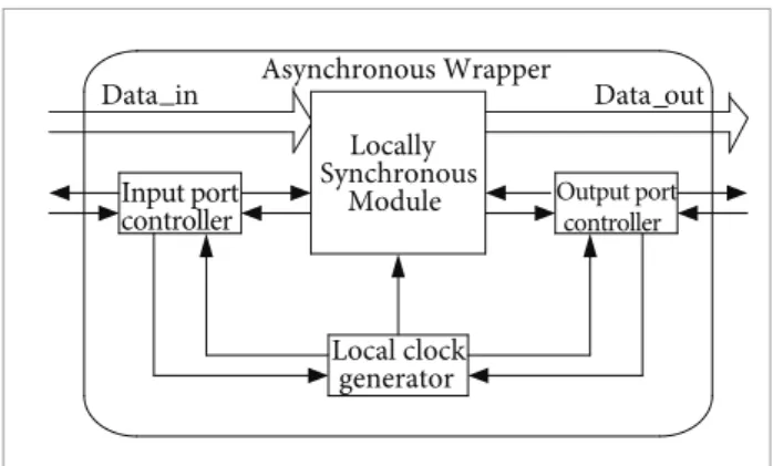
Concerning to this special situation and the features of both synchronous and asynchronous systems, intermediate solutions were proposed between “totally synchronous” and “totally asynchronous”, such as the Globally Asynchronous, Locally Synchronous methodology (GALS). he term GALS was irst used by Chapiro (1984), in his PhD thesis. A GALS system consists of many synchronous functional modules that communicate in the asynchronous form. In this paper, we refer to the GALS systems as digital systems partitioned in functional modules (that may be IPs), which carry their own individual clock signals and are unrelated between modules. An asynchronous communication scheme is provided for the communication between diferent modules with diferent clock domains. In order to handle the asynchronous communication between these modules, an interface circuit has to be added around each one of the synchronous modules, which is called an asynchronous wrapper (AW). he AW term was irst used by Bormann et al. (1997). his local interface may be built by using local clocks, FIFOs, asynchronous controllers (Input Ports, Output Ports) etc. Techan et al. (2007)
show diferent styles for asynchronous interfaces dedicated to GALS systems. Figure 1 shows a generic interface with a synchronous module as an example.
GALS systems have been successfully used in many implementations, including the Application Specific Integrated Circuit (ASIC) (Gurkaynak et al., 2006; Amini
et al., 2006; Miller et al., 2005) and Field Programmable Gate Array (FPGA) (Jia et al., 2005; Kumala et al., 2006; Yuan et al., 2005). Currently, FPGA devices have shown to be a common choice for implementing digital circuits (Muller-Glaser, 2004), growing considerably in recent years. High-performance FPGAs, with up to 50 million gates, can be easily found nowadays, therefore allowing complex digital systems, such as GALS, to be programmed on them (De Micheli, 2009) and to be implemented in CMOS technology, DSM.
Asynchronous interfaces that use communication ports are of main interest, once they allow removing the asynchronous handshake scheme from the synchronous modules, allowing the synchronous module to be developed using standard techniques of synchronous design. Although the GALS methodology has solved problems related to the global clock signal, the communication between modules is already performed in the asynchronous paradigm, therefore being subjected to all its inherent problems.
IMPLEMENTATIONS OF PORTS: DIFFERENT APPROACHS
Diferent kinds of ports have been synthesized in the logic synthesis style (Myers, 2004). As an example, the ports proposed by Amini et al. (2006) have been speciied in Signal Transition Graph (STG), which is a Petri-net-likespeiciication (Chu, 1987), being synthesized
Locally Synchronous
Module
Local clock generator
Output port controller
Input port controller
Asynchronous Wrapper
Data_in Data_out
in the Petrify tool (Cortadella et al., 1997). hese ports must meet the isochronic fork requirement (Myers, 2004), but the realization of this requirement in VLSI_DSM presents a high level of diiculty. Furthermore, the STG speciication, as well as its synthesis method, is not familiar to synchronous paradigm designers.
he ports proposed by Muttersbach et al. (2000), Muttersbach (2001), Reddy Ravi (2001) and Pontes
et al. (2007) were speciied in Extended Burst-Mode (XBM) and Burst Mode (BM). hese ports were implemented, respectively, in 3D (Yun et al., 1999) and minimalist (Fuhrer
et al., 1999) tools. hey interact with the environment in the generalized fundamental mode (GFM), requiring a timing analysis and being subjected to essential hazard, especially in the DSM technology. Concerning to this last drawback, the insertion of delay elements may be a possible solution (VLSI_DSM), but it degrades the testability and cycle-time of the system. he insertion of delay elements is not adequate when implementing GALS in FPGA as well, because these devices (FPGAs) are not designed to favor the insertion of delay elements.
AVOIDING ESSENTIAL HAZARD IN PORTS CONTROLLERS: INCREASING THE SYSTEM’S RELIABILITY
The XBM specification is quite interesting when describing port controllers, once it is not only “familiar” to synchronous paradigm designers, but also because the method that synthesizes ports described by XBM shows to be simpler when compared to the synthesis by STG (Myers, 2004). Yun et al. (1999) and Nowick (1993) proposed the insertion of delay elements on the feedback wires in order to avoid essential hazard in burst-mode controllers. Oliveira et al. (2008) proposed a sufficient condition that guarantees essential hazard-free operation on burst-mode controller without the need for extra delay elements, when mapped on VLSI_DSM or any type of LUT-based FPGA. The absence of delay elements is highly desirable when considering FPGA devices (difficulties in implementing this kind of elements) and, furthermore, in aerospace applications, in which the harsh environment must change the behavior of electronic components.
This paper proposes robust port controllers for asynchronous interfaces used in GALS style. They are completely free of essential hazard and are described
in the XBM specification. The robust controller design for asynchronous interfaces is proposed as a solution to the increasing demand for high reliablility aerospace electronic systems. The paper also shows that the method proposed by Oliveira et al. (2011) to synthesize BM controllers free of essential hazard is improved for XBM controllers. These proposed ports are implemented in the following architectures: “Huffman machine with feedback output” and “standard RS”. The use of both architectures enables a better performance of the system, besides being more reliable and providing safer operation for aerospace applications. A new AW for GALS with robust ports is also proposed. Once it is known that a major drawback in the design of asynchronous wrapper is the synthesis of these ports, the proposed AW proved to be very important and robust. These ports are easily implemented both in VLSI_DSM and LUT-based FPGA. Other advantages of this wrapper are: 1) total autonomy to the locally synchronous modules, when interacting with the proposed AW; and 2) its ports interact with the environment in the mode Ib/Ob, thus not requiring timing analysis and being more robust than the GFM mode. In this mode, a new input burst is immediately accepted when all signals of output burst change their values. All of these achieved features make the proposed architecture a good option for aerospace implementations, once it increases the reliability of the full system, overcoming some of the main challenges in this kind of industry.
DIFFERENT STYLES OF GALS DESIGN
WEAK SYNCHRONOUS INTERFACE
This style has three variants: a) heterochronous; b) mesochronous; and c) plesiochronous. In the heterochronous style (footer), the clocks of the synchronous modules run on different nominal frequencies (Techan et al., 2007). On the other hand, in the mesochronous style (from Greek, meso means average), the clocks show the same average frequency, but with different unknown phases, which are generated by the same oscillator (Techan et al., 2007). Finally, in the plesiochronous style (from Greek, plesio means “almost equal”), the clocks operate with equal nominal frequency, but being generated by different oscillators (Techan et al., 2007). These styles always require timing analysis, starting from the knowledge of the clocks and using FIFO as a base, phase adjusters and, sometimes, synchronizers. The advantage of these styles is to enable low latency and high frequency clocks. On the other hand, there is the need for a rigorous timing analysis. Figure 2 shows a mesochronous interface that uses a phase adjuster (timing recovery circuit – TRC).
PAUSIBLE CLOCK INTERFACE
his style, irstly proposed by Chapiro (1984), tackles the problem of metastability by interrupting the clock signal. When data are ready for transmission, the clock is interrupted, enabling data synchronization. he synchronous modules have pausible clock signals. Most oten, these clocks are locally generated using a ring oscillator and a mutual-exclusion circuit, or arbitrator, which properly generates the pause and restart of the clock (Yun et al., 1999). he potential advantages of this style are the robustness in the treatment of metastability and power reduction. On the other hand, the weakness of this style is the possibility of “deadlock” and “jitter” (Mullins et al., 2007). Diferent architectures have been proposed for pausible clocks, for example, the one involving FIFO (Techan et al., 2007). Figure 3 shows an architecture involving pausible clock as an example.
ASYNCHRONOUS INTERFACE
his style uses circuits known as synchronizers and handshaking signals. he synchronous modules have clocks running freely at diferent frequencies, without any prior knowledge about their timing. Data are synchronized from one clock domain to another. Some examples of data synchronizers are the well known “two registers”, or “double latches” (Mullins
et al., 2007), or some other more elaborated synchronization schemes, such as the “synchronization pipeline” (Sjogren
et al., 2000) and “FIFOs” (Dobkin et al., 2006). he proposed synchronizers do not totally eliminate failure due to metastability, once the probability of failure diferent of zero percent remains (Dobkin et al., 2006). he “two register” synchronizer presents as advantages its simplicity and robustness, but as a disadvantage there is an increasing area, power, and especially a high penalty in latency times, which leads to an increase of two clock cycles. Figure 4 shows the architecture of asynchronous interface as an example. Common Clock Reference
Sending
Module TRC ReceivingModule
Delay_wire1 Clock
Delay_wire2
Delay_data
Data Data_sync
Clock’
Figure 2. Mesochronous with TRC.
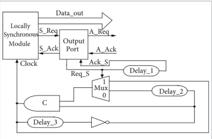
Locally Synchronous
Module Output
Port S_Req S_Ack
A_Req A_Ack
C 0
1 Clock
Req_S Ack_S Data_out
Delay_1
Delay_3
Delay_2 Mux
Figure 3. Pausible clock for FPGA described by Techan
et al. (2007).
Figure 4. Asynchronous interface based on FIFO.
Locally Synchronous
Module 1
Locally Synchronous
Module 2 FIFO
Clock1 Clock2
Rd_clk Wd_clk
Rd_en Wr_en
Full Empty
Rd_valid
COMMUNICATION CONTROLLERS (PORTS) GALS systems require asynchronous communication links, which can require two kinds of communication protocols: two or four stages handshaking. The ports can work as active (generating the “request” signal) or passive (generating the “acknowledge” signal). In GALS design there are two types of communication controllers: a) port of “demand”, b) port of “poll” (inquiry). In the port of demand, the data being transferred are immediately required after the communication. Therefore, in this type of controller the clock must be immediately stopped (paused) and reactivated (restarted) when communication is done. In the port of poll, the clock is not stopped immediately. It defines when it is “safe” to send the data. The clock is stopped (paused) only in cases when there is the need for additional time, in order to troubleshoot eventual metastability.
XBM-EHF SPECIFICATION: CONDITION
BM is a kind of specification based on a state transition graph which was first proposed by Davis et al., (1979), later formalized by Nowick (1993), and improved by Yun
et al. (1999) as XBM. It allows multiple input changes and is usually used to describe Mealy Asynchronous Finite State Machines (FSM). These machines interact with the environment in GFM. In GFM, a new input burst can only occur if the controller is stable (with no activity in the ports or in the lines). The XBM specification supports the BM specification, introducing two kinds of input signals: a) conditional signal that is sensitive to level, showing non-monotonic behavior; and b) “directed don’t care signals” that can activated concurrently with the output signals.
In this paper, the XBM specification is illustrated with the benchmark Biufifo2dma of the HP (see Fig. 5), with four inputs (cntgt1,dackn, fain,ok), two outputs (dreq,frout) and initial state 0. The description fain- dackn+/ frout+ in transition 4→3 means that the output
(frout: 0→1) will follow the input burst (fain: 1→0 AND dackn: 0→1). Signals not enclosed in angle brackets and
ending with + or — are “terminating”. Signals enclosed in angle brackets are “conditionals”, which are level sensitive with non-monotonic behavior. The input signals dackn,
fain and ok are transition sensitive signals (TSS). The level sensitive signal cntgt1 is used to describe the mutual exclusion between transitions 2→5 and 2→4. The “directed
don’t care signal” fain* in transition 2→4 means that fain
may either change its value or remain in its previous value. All state transition should have at least one signal called “compulsory”. A compulsory signal is an input signal that, in the previous state transition, is not directed to don’t care. A TSS input signal in a XBM specification is considered as a context signal in a transition A→B if it does not change its value during such transition (it is not on the label). On the other hand, it is considered as a trigger signal if it is labeled during this transition. The input burst of each state transition can be represented by an input transition cube (ITC). For example, the ITC in state transition 0→1 on Fig. 5 is cntgt1, dackn, fain, ok=2102 (the number 2 means“don’t care”). In this example, ok is a trigger signal, while dackn and fain are context signals (whose values are 1 and 0, respectively).
Deinition 1.1: Let A and B be a pair of total states in a
XBM speciication, and Ib/Ob be the input/output burst for the
A→B transition. Let Es be one “terminating” input (Es ∈ Ib).
Es is considered as an essential signal if it is a context signal on all transitions that address state A and is a trigger signal on the transition A→B.
For instance (see Fig. 5), there is not an essential signal in state transitions 0→1, 4→3 and 3→2 because they are trigger signals on transitions 5→0, 2→4 and 2→5. Signal ok is essential on transition 1→2, because it is a context signal on transition 0→1. On transitions 2→4 and 2→5,
dackn is essential signal.
Lemma 1.1 – (proof is presented by Oliveira et al. (2008))
A XBM speciication is essential hazard-free (XBM-EHF) only if for each state transition labeled by Ib/Ob, if Ob≠∅, there
must be, at least, one essential signal.
0
3
4 1
2 5
ok+ / frout+
fain+ / dreq+ frout-ok- fain- dackn+ /
<cntgt1->
fain* dackn- / dreq- <cntgt1+> fain* dackn- /
dreq-fain- dackn+ / frout+ fain+ /
dreq+
As an example, Fig. 6 shows the HP-mp-for-pkt benchmark described by a BM speciication. On all transition labels there is at least one essential signal. herefore, it is a BM-EHF speciication. Figure 7 shows the state low map of HP-mp-for-pkt. As shown by Oliveira et al. (2008), which applies the rule generalized Ungle to check for essential hazard, this states low map is subjected to essential hazard. he essential hazard depends on the code that the don’t-care assumes, when held the logic coverage free of logic hazard.
ESSENTIAL CUBE CONDITION
Lemma 1.1 is a necessary and suicient condition for an essential-hazard-free speciication, but not for hazard-free implementation. he super-state concept will guarantee the latter condition. According to Oliveira et al. (2008), the concept of super-state is presented. It is
used to obtain an implementation EHF. To simplify the implementation EHF, in this article we generalize the concept of super-state introducing the idea of essential cube.
Deinition 1.2: Consider an input burst I
b (a, b, ..n) and
an output burst Ob(x, y,..m). We call a super-state the set of single total states deined by all 0/1 combinations of a subset
SIb of the input burst signals, keeping all the remaining input signals and all the output signals constant.
Deinition 1.3: Consider a XBM-EHF speciication and
a super-state F of the state transition T,so that FÎ XBM-EH,
whereas T is labeled by Ib/Ob. We call essential cube of transition T all the total states related to the 0/1 combinations of input burst and output burst (Ib/Ob). Whereas the states not reachable in the cube T are encoded with the value of context signals, and trigger signals are don’t-care.
A super-state XBM flow map is derived from a XBM-EHF specification by applying definition 1.2 to all total states. The essential cube is composed of 2N states, in which
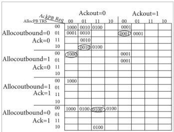
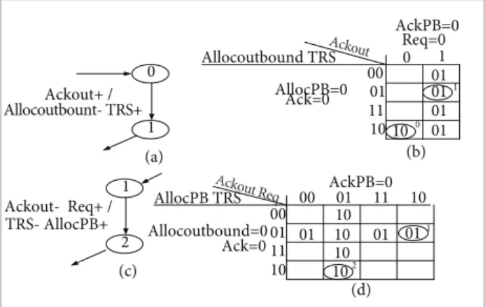
N is the total number of input signals plus the output signals that are labeled in a state transition. Figures 8a-d are part of the flow map for the BM specification described in Fig. 6. Cells in blue are used to compose super-states and essential cubes (applying the definition 1.3). For example, the 0→1 transition (see Fig. 8a,b and 9a,b) creates super-state 1 composed of two total states: AckPB Req Ackout Allockoutbound Ack AllocPB RTS=[0010001, 0000001]. State 0010001 is the final total state. Figure 9b shows the essential cube of the state transition 0→1, in which the next total states in blue are not reachable and belong to the essential cube. Due to the delays of gates and wires, the state totals which not are reachable can become reachable. For example, the 1→2 transition (see Fig. 8c,d and 9c,d) creates super-state 2, composed of four total states: AckPB Req Ackout Allockoutbound Ack AllocPB RTS= [1000010, 1100010 ,0100010,0000010]. State 0100010 is the final total state. Figures 9b,d respectively, show the essential cubes of the transitions 0→1 and 1→2. Lemma 1.2 and theorem 1.1 show the robustness of our controls.
Lemma 1.2 – Let T (B→A) be a state transition of
XBM-EHF speciication labeled by Ib/Ob and let an input signal any
Is ∈ Ib and an output signal any Os ∈ Ob. If T is described by an essential cube, then in whatever order and whatever the time of arrival of Is and Os activation the total generated states belong to the essential cube T, and they all lead to the inal total state A.
Ackout+ / Allocoutbound - TRS+ Allocoutbound + Ack
-Ackout - Req+ / TRS -AllocPB + AckPB - Req- /
AckPB+ / AllocPB - Ack +
0
1
2 3
Figure 6. BM-EHF Speciication.
Ac kPB Req
0100
1000
0100
3 0100 0100 10
11 01 00
0001 0001 1000
Allocoutbound=1
0
0001 00
10 11 01
00 01 11 10 00 01 11 10
0010
0100 0010 0010
0001 0010 0001 0001
AllocPB TRS
Allocoutbound=0
Ackout=0 Ackout=1
1
2
10 11 01 00
1000
Allocoutbound=1
10 11 01
00 1000 0100
Allocoutbound=0 Ack=0
Ack=0
Ack=1
Ack=1
Proof: As a cube essential, T consists of 2N total states,
in which N is the sum of the signals that compose the input burst (Ib) and the output burst (Ob). As the next states not reachable in the transition B→A are encoded in the way in which the signals of Ib and Ob are don’t-care, then whatever combination of activations of the signals Is and Os in T, the total states generated will belong to the cube essential T and lead to inal state A, therefore the cube essential is free of essential hazard.
heorem 1: he XBM-EHF speciication has an EHF
implementation in the “Hufman machine architectures with feedback output” or “standard RS” if ∀ state transition T (B→A) ∈ XBM-EHF, all your activation is covered by the cube essential T.
Proof: Lemma 1.2 says that if the XBM speciication is
EHF, then whatever the state transition T∈XBM has a cube essential T. As the context signals in T transition remains as a constant value in all the next states, which are reachable and not reachable in the cube essential, then regardless of the delays of gates and wires of the architectures, the activation of the next state belongs to the cube essential. As essential cube is EHF according to lemma 1.2, then the implementations on both architectures are EHF.
ASYNCHRONOUS WRAPPERS: ARCHITECTURE he main objective of the proposed architecture is to provide a weak interface interaction between the locally synchronous module (LSM) and the asynchronous interface. Figure 10 shows the two diferent variables, “data available” and “data accept”, as the only ones used for communication between LSM and the interface. When data available=‘1’, data is ready to be transmitted, while when data accept=‘1’ the
data was received. Our architecture is based on the architecture proposal described by Reddy Ravi (2001).
Figure 11 shows the architecture of the proposed output communication control, which implements the weak interaction between the interface and the LSM, while Figs. 12 and 13 show the proposed input and output asynchronous wrapper, respectively, with the insertion of a gated clock generator. Finally, Fig. 14 shows the full proposed AW that receives and transmits data.
Figure 8. Part of BM speciication: a) transition 0→1; b) low map; c) transition 1→2;d) low map.
0 1 01 01 01 01 10 10 11 01 00 Allocoutbound TRS 0 1 AllocPB=0Ack=0 AckPB=0 Req=0 (b) 0 1 Ackout+ / Allocoutbount- TRS+ (a) 00 10 10 10 10 01 01 01 10
11 01
00 01 11 10
1 2 AckPB=0 Allocoutbound=0 Ack=0 (d) AllocPB TRS 1 2 Ackout- Req+ / TRS- AllocPB+
(c)
Ackout Req
Ackout Locally Synchronous Module Locally Synchronous Module LCLK Data Available Output Interface RT AT Asynchronous Wrapper DATA LCLK Data Accept RR AR Asynchronous Wrapper DATA Input Interface (a) (b)
Figure 10. Locally synchronous module with weak interface: a) output; b) input.
Figure 11. Communication control of output.
LCLK Data Available Q Q SET CLR D D Q Q Output PORT (AFSM) RT AT R_CLK A_CLK En_D Latch Reset Communication control
Figure 9. Part of BM low map with ESS and EC: a) 0→1;
b) 1→2. Ackout 0 1 01 01 01 01 10 10 11 01 00 Allocoutbound TRS 0 1 AllocPB=0 Ack=0 AckPB=0 Req=0 00xx 00xx 00xx (a1) Essential super state Ackout 0 1 01 01 01 01 10 10 11 01 00 Allocoutbound TRS 0 1 AllocPB=0 Ack=0 AckPB=0 Req=0 00xx 00xx 00xx (a2) Essential Cube Ack out Req 00 10 10 10 10
01 01 01
10 11 01 00 10 11 01 1 2 AckPB=0 Allocoutbound=0 Ack=0 (b2) 00xx AllocPB TRS 00xx 00xx 00xx 00xx 00xx 00xx 00xx 00xx Ackout Req 00 10 10 10 10
01 01 01
GATED-CLOCK GENERATOR
In this paper, a gated-clock generator (GCG) composed basically by two synchronizers and a gated-clock is also proposed. Figure 15 shows the timing diagram of the proposed GCG with the activation and deactivation of signal GCLK. While Fig. 16 shows the architecture of GCG, Fig. 17 shows the topology of the gated-clock and Fig. 18 shows the topology of its synchronizer. he stopping (pause) of the GCLK signal occurs when RCLK switches 0→1 and ater two clock cycles the signal “Stop” switches 0→1, thus determining the stopping (interruption) of signal GCLK.
DESIGN: PORTS (AFSM)
The input/output ports used in the proposed AW were previously proposed by Muttersbach et al. (2000) and Muttersbach (2001). They are described in the XBM specification (as shown in Figs. 19 and 20). The XBM specification of the input/output ports meets the essential signal concept, therefore XBM_EHF.
Locally Synchronous
Module
GCLK Data Available
DATA TRANSMITTER
Q Q SET
CLR D
D Q
Q
Output PORT (AFSM)
RT
AT
Gated-Clock Generator
R_CLK A_CLK En_D
Latch
Reset
OUTPUT INTERFACE
CLK
Figure 12. Proposed output asynchronous wrapper.
Q QSET
CLR D
Locally Synchronous
Module
GCLK
Data Accept DATA RECEIVER
D Q Q AR
RR
R_CLK A_CLK
En_D
Latch
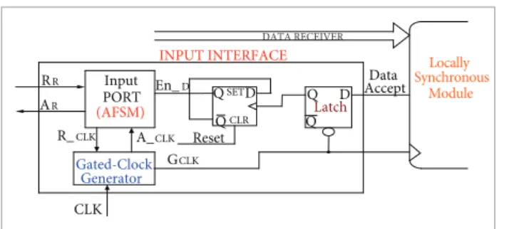
Reset INPUT INTERFACE Input
PORT (AFSM)
Gated-Clock Generator
CLK
Figure 13. Proposed input asynchronous wrapper.
Figure 14. Proposed asynchronous wrapper: with I/O.
Locally Synchronous
Module
DATA DATA
Gated-Clock Generator
GCLK Input
Control
Data Accepts
Output Control
Data available Asynchronous Wrapper
R1_CLK
A1_CLK RR
AR
RT
AT R2_CLK
A2_CLK Latches
CLK
Stop
A_CLK CLK
R_CLK
GCLK
Figure 15. Timing diagram: gated-clock generator.
Synchronizer-1 Synchronizer-2
Gated-Clock
GCLK
CLK
Stop-1 Stop-2
R1_CLK A1_CLK R2_CLK A2_CLK
Figure 16. Architecture of the proposed gated-clock generator.
Q Q D
Latch
Stop1
GCLK
CLK
Stop2
Figure 17. Topology of the gated-clock
Q Q SET
CLR D
Q Q SET
CLR D R_CLK
Stop A_CLK
CLK
PROCEDURE: SYNTHESIS OF PORTS
he ports designing method starts from the XBM description and is synthesized in four steps:
• Use the algorithm of Yun et al. (1999) and derive the minimum set of XBM low charts;
• Encode XBM low tables using the adjacency diagram (Unger, 1969);
• For each coded XBM low table, insert the essential super-states, as seen in the previous section;
• Perform the logic minimization, logic-hazard-free, for each “non-input” signal in the “standard RS” and “machine Hufman with output fed back” architectures (Oliveira et al., 2008).
Figure 21 shows the state flow map of the output port, with the introduction of a state signal ‘Z’ to solve conflicts, while Fig. 22 shows all the minterms (black and blue) used
0 1 2 3 4 5 6 7
En_D+ RR+ / R_CLK+
A_CLK+ / AR+
RR- / R_CLK- AR -A_CLK- RR* /
En_D- RR+ / R_CLK+
A_CLK+ / AR+ RR- / R_CLK- AR
-A_CLK- RR* /
Figure 19. XBM Speciication: input port described by Muttersbach et al. (2000) and Muttersbach (2001).
2 3 4 5 6 7 8 1
A_CLK+ / R
T-AT- / R_CLK
-A_CLK -En_D- / RT+ AT+ / R_CLK +
A_CLK+ / R T-A T- / R_CLK -A_CLK- En_D+ /
RT+
A T+ / R _CLK+ 0
En_D+ / RT+
Figure 20. BM Speciication: output port described by
Muttersbach et al. (2000) and Muttersbach (2001).
A_ CLKAT 101 111 111 110 110 00 10 11 01 00 10 11 01 00 10 11 01 000 010 000 010 011 011 001 001 110 000 000 R_CLK RT Z=0 En_D=0 En_D=1 0 8 1 2 3 00 10 11 01 00 10 11 01 00 10 11 01 101 010 100 100 100 100 R_CLK RT Z=1 En_D=0 En_D=1 5 6 7 4 A_ CLKAT
Figure 21. State low map: output port subject to essential hazard.
A_CLK AT
101 111 111 110 110 00 10 11 01
00 000 01 11 10 00 01 11 10
010 000 010 011 011 001 001 110 000 000 R_CLK RT Z=0 En_D=0 En_D=1 0 8 1 2 3 00 10 11 01
00 101 01 11 10 00 01 11 10
010 100 100 100 100 R_CLK RT Z=1 En_D=0 En_D=1 5 6 7 4 A_CLK AT
00x 0x1 01x 10x 1x1 1x1 0x0 0x0 10x 10x 1x0 1x0 00x 00x
Figure 22. State low map: output port essential hazard-free.
A_CLK AT R_CLK RT R_CLK RT x x x x x 00 10 11 01
00 0 01 11 10 00 01 11 10
0 0 0 0 0 0 0 1 0 0 Z=0 En_D=0 En_D=1 0 8 1 2 3 00 10 11 01
00 x 01 11 10 00 01 11 10
0 x 1 x x Z=1 En_D=0 En_D=1 5 6 7 4 A_CLKAT 0 0 0 x x x 0 0 x x x x 0 0
F SET = En_D A_CLK AT R_CLK
Figure 23. Karnaugh map: coverage hazard-free of signal
Z (FSET).
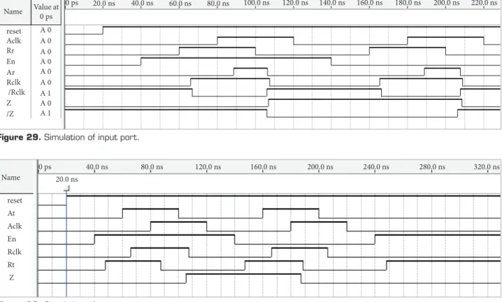
DISCUSSION & SIMULATION
Oliveira et al. (2011) present a list of advantages of the GALS system, which leads to the conclusion that GALS design can play a relevant role in the future of digital design in all kind of applications, including aerospace ones. However, a major drawback to this use is the asynchronous interface.
Focusing on this kind of application, the proposed hazard-free asynchronous interface proved to have a great potential, being highly desirable for the aerospace industry, once it overcomes the main challenges of this industry, thus increasing the reliability of the full system. In the treatment of essential hazard, our ports support any type of mapping either for VLSI_DSM or PLDs devices. It follows the Delay Insensitive model (DI) (Myers, 2004), restricted to interact with the environment in GFM, but without the insertion of any delay elements. his interface allows working in Ib/Ob mode, showing that the DI model is more robust than the QDI model, therefore not needing to meet isochronic fork requirements. An interface presenting similar properties was not found in literature. Figures 29 and 30 show simulations of I/O ports of the proposed AW, which show that the proposed architecture satisies the XBM speciication, are hazard-free and robust. A_CLK AT
R_CLK RT R_CLK RT 0 0 0 0 0 00 10 11 01
00 x 01 11 10 00 01 11 10
x 1 x x 0 x x 0 x x Z=0 En_D=0 En_D=1 0 8 1 2 3 00 10 11 01
00 0 01 11 10 00 01 11 10
1 0 0 0 0 Z=1 En_D=0 En_D=1 5 6 7 4 A _CLK AT
x x x 0 0 0 x x 0 0 0 0 x x
F RESET = En_D A_CLK AT R_CLK
Figure 24. Karnaugh map:coverage hazard-free of signal Z
(FRESET).
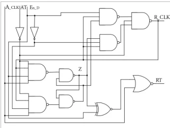
Figure 28. Logic circuit: input port hazard-free.
RR A_CLK En_D
Z
AR
R_CLK A_CLK AT
R_CLK RT R_CLK RT 0 1 1 1 1 00 10 11 01
00 0 01 11 10 00 01 11 10
1 0 1 1 1 0 0 1 0 0 Z=0 En_D=0 En_D=1 0 8 1 2 3 00 10 11 01
00 0 01 11 10 00 01 11 10
1 0 0 0 0 Z=1 En_D=0 En_D=1 5 6 7 4 A_CLK AT
0 x 1 0 x x x x 0 0 x x 0 0
R_CLK = AT + En_D Z R_CLK + En_D Z R_CLK
Figure 25. Karnaugh map: coverage hazard-free of signal
R_CLK.
A_CLK AT
1 1 1 0 0 00 10 11 01 00 10 11 01 00 10 11 01 0 0 0 0 1 1 1 1 0 0 0
R _CLK RT
Z= 0 En_D=0 En_D=1 0 8 1 2 3 00 10 11 01 00 10 11 01 00 10 11 01 1 0 0 0 0 0
R _CLK RT
Z= 1 En_D=0 En_D=1 5 6 7 4 A_CLK AT
x 1 x x 1 1 0 0 x x 0 0 x x
RT = A _CLK (En _D Å Z )
Figure 26. Karnaugh map: coverage hazard-free of signal RT.
AT
A_CLK En_D
R_CLK
RT Z
CONCLUSION
GALS systems implemented in VLSI_DSM are an interesting design style for SoCs, however, typical problems concerning the asynchronous interface, especially for AW design, proves to be major drawbacks. In relation to aerospace applications, in which reliability and safety are major constraints, these drawbacks are prohibitive. Concerning this situation, a new architecture to AW was proposed in order to overcome the previously discussed problems, showing to be a good option for those designers who need to implement GALS in VLSI_DSM, including for aerospace applications, once it improves the reliability of the system, thus eliminating essential hazards. he achieved results showed that the proposed architecture is completely free
Name Value at0 ps
reset Aclk Rr En Ar Rclk /Rclk Z /Z
A 0 A 0 A 0 A 0 A 0 A 0 A 1 A 0 A 1
0 ps 20.0 ns 40.0 ns 60.0 ns 80.0 ns 100.0 ns 120.0 ns 140.0 ns 160.0 ns 180.0 ns 200.0 ns 220.0 ns
Figure 29. Simulation of input port.
Name
reset At Aclk En Rclk Rt Z
0 ps 20.0 ns
40.0 ns 80.0 ns 120.0 ns 160.0 ns 200.0 ns 240.0 ns 280.0 ns 320.0 ns
Figure 30. Simulation of output port.
of essential hazard and allows full autonomy for the locally synchronous modules. It follows the DI model, interacts with the environment in GFM without the need to insert any delay elements, as suggested by the previous papers found in literature, and allows working in Ib/Ob mode, proving to be more robust than the QDI model and, therefore, not needing to meet isochronic fork requirements nor requiring timing analysis. Since an interface presenting similar properties was not found in literature, the proposed architecture showed to have a great potential of implementation in all VLSI_DSM systems, including the aerospace ones, in which the harsh environment imposes additional challenges to the designers. Future work leads to a robust asynchronous interface for the implementation of GALS, involving FIFO and an application aimed for sotware-deined radio.
REFERENCES
Amini, E., Najibi, M. and Pedram, H., 2006, “Globally asynchronous
locally synchronous wrapper circuit based on clock gating”, Emerging
VLSI Technologies and Architectures, IEEE Computer Society Annual
Symposium, Vol.00, pp. 2-3.
Bertuccelli, L.F,, 2008, “Robust Decision-Making with Model Uncertainty in Aerospace Systems”, Ph.D. thesis, MIT, September, 2008.
for Heterogeneous Systems,” Proc. Int. Conf. Computer Design (ICCD), pp. 307-314.
Chapiro, D.M., 1984, “Globally-Asynchronous Locally-Synchronous Systems”, PhD thesis, Stanford University, October, 1984.
Chu, T.A., 1987, “Synthesis of Self-Timed VLSI Circuits from Graph-Theory Speciications”, Ph.D. thesis, Dept. of EECS, MIT, June, 1987.
Cortadella, J. et al., 1997, “Petrify: A tool for manipulating concurrent
speciications and synthesis of asynchronous controllers”, IEICE Trans. Inf. Syst., Vol.E80-D, No. 3, pp. 315-325.
Davis, A.L. et al., 1979, “A data-driven machine architecture suitable
for VLSI implementation”, In C.L. Seitz, editor, Proc. of the Caltech Conf. on Very Large Scale Integration, pp. 179-194.
De Micheli, G. 2009, “An Outlook on Design Technologies for Future Integrated Systems”, CAD of Integrated Circuits and Systems, Vol. 28, No.6, pp. 777-789.
Dobkin, R., Ginosar, R. and Sotiriou, C.P., 2006, “High Rate Data Synchronization in GALS SoCs”, TVLSI, Vol. 14, No. 10, pp. 1063-1074.
Friedman, E.G., 2001, “Clock distribution networks in synchronous digital integrated circuits”, Proc. IEEE, Vol. 89, No. 5, pp. 665-692.
Fuhrer, R.M. et al., 1999, “Minimalist: An environment for the
Synthesis, veriication and testability of burst-mode machines”, Technical Report, Columbia University, TR-CUCS-020-99.
Ginosar, R., 2003, “Fourteen ways to fool your synchronizer”, Proc. of ninth Int. Symp. On Async. Circuits and Systems, Vancouver, British Colombia, Canada, pp. 89-96.
Gurkaynak, F.K. et al., 2006, “GALS at ETH Zurich: Success or
Failure?”, Proc. 12th IEEE Int. Symposium on Asynchronous Circuits
and Systems, pp. 150-159.
Hardt, W. et. al., 2000, “Architecture Level Optimization for
Asynchronous IPs”, Proc. 13th Annual IEEE Int. Conf. ASIC/SOC,
pp.158-162.
Jain, A. et al., 2001, “A 1.2 GHz alpha microprocessor with 44.8
GB/s chip pin bandwidth”, IEEE Int. Solid-State Circuits Conf. Tech. Dig., pp. 240–241.
Jia, X., Vemuri, R., 2005, “Using GALS architecture to reduce the impact of long wire delay on FPGA performance”, Proc. of the Asia and South Paciic Design automation Conf., pp. 1260-1263.
Krstic, M. et al., 2007, “Globally Asynchronous, Locally Synchronous
Circuits: Overview and Outlook”, IEEE Design & Test of Computers, Vol. 24, pp. 430-441.
Kumala, A. et al., 2006, “Reliable GALS Implementation of MPEG-4
Encoder with Mixed Clock FIFO on Standard FPGA”, Int. Conf. on Field Programmable Logic and Application, pp. 1-6.
Martin, A.J. and Nystrom, M., “Asynchronous Techniques for
System-on-Chip Design”,Proc. of the IEEE, Vol.94, No. 6, pp. 1089-1120.
Miller, S.P. et al., 2005, “A Methodology for the Design and Veriication
of Globally Asynchronous/Locally Synchronous Architectures”, NASA/ CR-2005-213912, pp. 1-35.
Muller-Glaser, K.D. et. al., 2004, “Multiparadigm Modeling in
Embedded Systems Design”, IEEE Trans. on Control Systems Technology, Vol. 12, No. 2.
Mullins, R. and Moore, S., 2007, “Demystifying Data-Driven and Pausible Clocking Schemes”, Proc. of ASYNC’07, pp. 175-185.
Muttersbach, J., Villiger, T. and Fichtner,W., 2000, “Practical Design
of Globally-asynchronous Locally-synchronous System”, Proc. IEEE 6th
Int. Symposium Advanced Research in Asynchronous Circuits and Systems, pp. 52-59.
Muttersbach, J. 2001, “Globally-Asynchronous Locally-Synchronous Architectures for VLSI Systems”, Ph.D. Thesis, ETH, Zurich, 2001.
Myers, C.J. 2000, “Asynchronous Circuit Design”, Wiley & Sons, Inc., 2004, 2nd edition.
Nowick, S.M, 1993, “Automatic Synthesis of Burst-Mode Asynchronous Controllers”, PhD thesis, Stanford University, 1993.
Oliveira, D.L. et al., 2008, “Burst-Mode Asynchronous Controllers
on FPGA”, Int. Journal of Reconigurable Computing, Vol. 2008, pp. 1-10.
Oliveira, D.L. et al., 2011, “Synthesis of Robust Conrollers for GALS_
FPGA from Multi-Burst Graph Speciication”, Proc. IEEE VII Southern Conference on Programmable Logic (SPL), pp. 123-129.
Pontes, J. et al., 2007, “SCAFFI: an Intrachip FPGA asynchronous
interface based on hard macros”, 25th Int. Conf. on Computer Design,
pp. 541-546.
Reddy Ravi, A., 2001, “Globally-Asynchronous, Locally-Synchronous Wrapper Conigurations for Ponint-to-Point and Multi-Point Data Comunication”, Masters of Science, University of Central Florida, 2001.
Sjogren, A.E. and Myers, C.J., 2000, “Interfacing Synchronous and Asynchronous Modules within a High-Speed Pipeline”, IEEE Transactions on VLSI Systems, Vol. 8, No. 5, pp. 573-583.
Sues, R.H. et al., 2005, “Reliability-Based MDO for Aerospace
Systems”, AIAA-2001-1521, pp. 1-8.
Techan, P., Greenstreet, M. and Lemieux,G., 2007, “A Survey and Taxonomy of GALS Design Styles”, IEEE Design & Test of Computers, Vol. 24, pp. 418-428.
Unger, S.H. 1969, “Asynchronous Sequential Switching Circuits”, John Wiley & Sons Inc.
Yuan, L. et al., 2008, “Research on the Problems of Satellite Borne
FPGA Based Finite State Machine”, 2nd Int. Symposium on Systems
and Control in Aerospace and Astronautics (ISSCAA), pp. 1-4.
Yun, K.Y. and Dill, D.L., 1999, “Automatic Synthesis of Extended Burst
-Mode Circuits: Part I (Speciication and Hazard-Free Implementation) and Part II (Automatic Synthesis)”, IEEE Trans. on CAD of Integrated Circuit and Systems, Vol. 18:2, pp. 101-132.