Anomalous Blueshift in Vertially Coupled InAs/GaAs
Quantum Dots Using InGaAs Strain-Reduing Layers
M. J. daSilvaand A.A. Quivy
InstitutodeFsiadaUniversidadedeS~aoPaulo,
Laboratoriode NovosMateriaisSemiondutores
CP66318,05315-970 S~aoPaulo,SP,Brazil
Reeivedon23April,2001
The vertial oupling ofInAsquantumdots and their appingwith In0:1Ga0:9As layers were
in-vestigatedinorderto shift theoptialemission ofthe struturestowardlongerwavelengths. We
observedthatbothwaysannotbeusedsimultaneouslybyjustreplaing partoftheusualGaAs
spaer layerby In
0:1 Ga
0:9
Asbeause the intermixingof Gaand Inatomsis enhaned instaked
layersandausesablueshiftoftheemissioninsteadoftheexpetedredshift.
I Introdution
The study of low-dimensional semiondutor
het-erostrutures is one of the most important topis in
Solid-State Physisas aonsequene of their
applia-tiontooptoeletronidevieslikelight-emittingdiodes
and lasers. A problem of urrent interest in this
eldisthepossibilityofextendingtheoptial-emission
range of GaAs-based devies up to 1.3m, whih is
a point of minimal attenuation of the optial bers.
InGaAs/GaAs quantum wells (QWs) annot be used
to reahthe required rangeof wavelengths beauseof
the limitations imposed by the two-dimensional (2D)
strainedgrowth. Reently,however,InAs/GaAs
quan-tum dots (QDs) grown by moleular beam epitaxy
(MBE)werepointedoutasareliablemannerto reah
this goal. When a thin InAs layer is deposited on a
GaAs(001) substrate, the initial growth proeeds
un-der2Dstrainedonditionsandtheelastienergyofthe
systemanberelaxedbyforming smalloherentInAs
islands at the surfae when the thikness of the
epi-taxiallayerslightlyexeedsaritialvalue(1.6MLs).
When these islands are overed by GaAs,they at as
quantumdots,exhibitingathree-dimensional(3D)
on-ning potential, and emit within the 1.0-1.2mrange
at room-temperature. Twoapproaheshavebeen
sug-gestedtoextendtheiremissionupto 1.3m. Therst
oneis thevertialoupling oflosely-stakedlayersof
QDs (separatedby GaAslayers) that takesadvantage
ofthenaturaltendenyoftheislandstoalignvertially
[1℄inordertoprodueaneetivepotentialwherethe
eletronilevelsareredshifted withrespettotheones
ofasinglelayerofQDs. Thisvertialorderinghasthe
the islands. The seond method uses asinglelayerof
InAs/GaAs QDs apped by a InGaAs lm that ats
asastrain-reduinglayer[2℄andpromotesaredshiftof
theeletronilevels. Bothmethodshaveamajor
draw-bak. Inorder to reah the1.3mregion, thevertial
ouplingrequiresalargenumberofQDlayersthat
on-siderably inreases the onentration of non-radiative
enters. TheappingofasingleQDlayerwithInGaAs
is eÆient to tune the emission toward longer
wave-lengths,but thewidesizedistribution oftheQDsin a
single layerbroadens the luminesenespetra (up to
90meV) and is disadvantageous to most of the
high-performaneoptialdevies.
Inthiswork,weinvestigatedthepossibilityof
om-bining both approahes to produe vertially oupled
InAs QDs separated by thin spaer layers where part
of the GaAs material was substituted by InGaAs. In
this way, weexpeted to takeadvantageofthe better
homogenizationofthestruturesprovidedbythe
stak-ing proedure andof thefaster tuning oftheemission
bytheInGaAsstrain-reduinglayersinordertoobtain
samplesemittingaround1.3mwithareduednumber
ofinterfaesandanarrowerlinewidth.
II Samples and experimental
setup
All the samples disussed here were grown in aMod.
GenIIMBEsystemonGaAs(001)epi-readysubstrates.
A 0.2m-thik GaAs buer layer was deposited at
580 o
C before the growth ofanyof thestrutures that
layersweredepositedat500 o
CtoavoidInrevaporation.
TheGa,InandAsuxesweresuppliedatarateof1.0,
0.05and2.5MLs/s,respetively,exeptwhenspeied
dierently. The samples were optially haraterized
byphotoluminesene(PL)at2Kandatroom
temper-ature, and strutural measurementsweredone by
9000
10000
11000
12000
13000
14000
15000
16000
D
C
B
A
Height(Å) Density (x10
9
cm
-2
)
2K
A 18 180
B 25 100
C 70 30
D 110 1
P
L
In
te
n
s
ity (a
rb
. u
n
its
)
Wavelength (Å)
Figure 1. 2K PL spetra of a single 2.4ML-thik InAs
QD layer grown with a In delivery rate of A) 0.1ML/s,
B) 0.08ML/s, C) 0.05ML/s and D) 0.005ML/s. The
in-set shows the height and densityof the QDs as measured
byatomiforemirosopyonsimilarsampleswithoutthe
300
A-thikGaAsaplayer.
ross-setion transmission eletron mirosopy
(XTEM).
III Results and disussion
Thesimplestwaytoredshifttheoptialemissionofthe
QDsisgrowingstrutureswithalargersize. Thatan
beahieved,within somelimits,by modifyingthe
dif-fusion length of the In adatoms that mainly depends
on the In delivery rate, the V/III ux ratio and the
substrate temperature used to deposit the InAs lm.
Figure 1showstheredshiftobtainedinthe rstsetof
samples where theInAs growth ratewasvaried. The
maindrawbakofthisapproahisthat,whenthesizeof
thestrutures beomeslarger,theirdensityis redued
and is no longer adequate for optoeletroni
applia-tions.
Aseondwaytoredshifttheoptialemissionofsuh
strutures isto redue thestrainof thesystem
result-ingfromthelattiemismathbetweenInAsandGaAs.
Figure2showsthePLspetraoftheseondsetof
sam-pleswherea2.4ML-thikInAsQDlayerwasappedby
In
0:1 Ga
0:9
Asinordertoreduethestrainoftheislands.
Eah sample had aInGaAs ap of dierent thikness
andreeivedanextralayerofGaAstoompleteatotal
ap-layerthiknessof300
A.Itislearfromgure2that
thestrainredutionahievedbytheIn
0:1 Ga
0:9
Aslayer
mostof theeetisobtainedforaIn
0:1 Ga
0:9
As
thik-nessaround25
Athatorrespondstoslightlymorethan
halfoftheheightoftheseburiedQDs[3℄.
Basedontheexperimentalresultsofbothprevious
setsofsamples,athirdsetwasgrownwhereseveralQD
layerswerestakedandappedaordingtosampleG.
Atotalspaerlayerof 50
Awas used between two
10000
10500
11000
11500
12000
12500
13000
b
a
H
G
F
E
36meV
300K
60mW
P
L
In
te
n
s
ity (a
rb
. u
n
its
)
Wavelength (Å)
Figure 2. 300K PL spetra of a single2.4ML-thik InAs
QDlayerapped by aIn0:1Ga0:9Aslayerwith athikness
aequalto E) 0
A F) 10
A G) 25
A and H)50
A. Finally, a
GaAs layer was deposited to omplete the total ap-layer
thiknessof300
A(=a+b).
onseutiveQDlayerssinethatspeiseparation
pre-viouslyprovidedagoodeletroniouplingforstaked
QDslayersgrowninthesameonditionsbutseparated
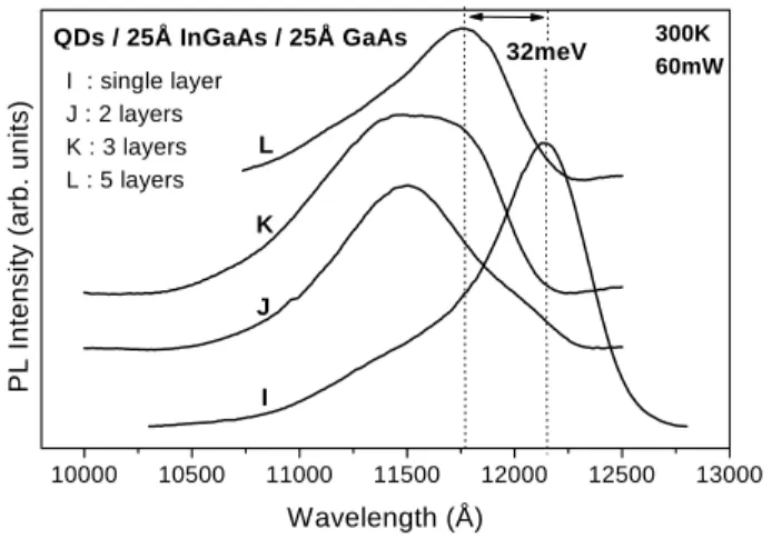
by a GaAs layer [3℄. It an be seen in gure 3 that
the three samples ontaining staked layers (J-L) are
blueshiftedwithrespettothereferenesample(I),
un-likeexpeted,but there exists asystematiredshiftof
thestakedsampleswithrespettosampleJwhenthe
numberofstakedlayersinreases.
The behavior observed in gure 3 an be
qualita-tivelyunderstoodonsideringthefollowingmodel. An
unappedInAsQDhasanequilibriumsizeand
ompo-sitionthat minimizethesurfaefreeenergyofthe
sys-temforspeistrainandgrowthonditions. Whenthe
islandisapped,anadditionalstressisimposedwhih
modies the equilibrium onditionof the newsystem.
Toreovertheminimal-energy ondition,an
intermix-ingeettakesplaeduringthegrowthoftheaplayer
andInatomsoftheislandaresubstitutedbyGaatoms
ofthegrowingaplayer. Thisphenomenon leadstoa
smallerandGa-rihislandthatyieldsablueshiftofthe
optial emission with respet to an unapped QD [4℄.
Theshrinking of apped InAsQDs anbelearly
ob-servedin ross-setion TEMimages that show islands
withabouthalf ofthevertialsize of free-standing
is-lands grownin the sameonditions (gure 4). When
several QD layersare staked, the equilibrium
onse-upper QDlayer, as onrmedin gure4b. Whenthe
InGaAs and GaAs ap layersof the referene sample
are grown, kineti and thermodynami onsiderations
duringdepositionditatethestrengthandextentofthe
intermixinginordertominimizethefreeenergyofthe
system, leading to spetrum I of gure 3. However,
whenaseond QDlayerisgrownatop(J), thestrain
10000
10500
11000
11500
12000
12500
13000
L
K
J
I
QDs / 25Å InGaAs / 25Å GaAs
32meV
300K
60mW
I : single layer
J : 2 layers
K : 3 layers
L : 5 layers
P
L
In
te
n
s
ity (a
rb
. u
n
its
)
Wavelength (Å)
Figure3. 300KPLspetraofstakedQDlayersgrown
a-ording tosampleG.ThenumberofstakedQDlayers in
eahsampleisI)1,J)2,K)3andL)5.
Figure4. (a)High-resolutionTEMimageofafree-standing
InAsQDgrowninthesameonditionsassampleC(b)Dark
eld(400)TEMimageoffourpairsofQDlayersseparated
by500
AofGaAs. TheGaAsspaerbetweeneahQDlayer
of a pairis 50, 100, 150 and 200
A (from top to bottom).
TheoverlapofthestraineldfromeahQDlayerofapair
isvisible.
onguration of the system is modied and turns to
be the driving fore to indue further intermixing in
the underneath QD layer, yielding even smaller and
more Ga-rih islands. Sine the top QD layer is also
aetedbythestraineld ofthelowerlayer(the QDs
are slightly larger)andthe intermixingis strongerfor
larger QDs, the whole system will have its emission
blueshiftedwithrespettothereferenesample.
How-vertialeletroniouplingbeomesmoreeetiveand
aredshiftoftheemissionisobserved(K-L).
IV Conlusion
Using PL measurements, we observed that staks of
InAsQDlayersalternatedwithInGaAsstrain-reduing
spaers arenot ableto shift theusual emission of the
strutures toward 1.3m as would be expeted. The
blueshiftdetetedinthePLspetraindiatesarelevant
intermixingduringtheappingandstakingproesses.
The driving fore for theexhange of In atoms of the
buriedQDsby Gaatoms ofthe aplayerseemsto be
related to the penetration of the strain eld oming
from the upperQD layersof the stak. Ifboth
meth-odshavetobeusedtogetherinordertoshifttheoptial
emissionofthesamplestowardlongerwavelengths,the
intermixinghasto beredued. Sine thephenomenon
is thermallyativated [5℄, onepossiblewayto ahieve
thatisbykinetiallylimitingtheproessusingalower
substratetemperature.
Aknowledgments
We are grateful to FAPESP for nanial support
(grants 99/08979-7, 99/01225-7, 98/14489-0), to the
\LaboratoriodeFilmesFinosdoIFUSP"fortheSPM
faility(FAPESP pro. 95/05651-0)andto the
\Lab-oratorio de Mirosopia Eletr^onia (LME/LNLS)" for
theTEMfaility.
Referenes
[1℄ G.S.Solomon,J.A.Trezza,A.F.Marshall,J.S.Harris
Jr,Appl.Phys.Lett.,76,952(1996).
[2℄ Y. Nakata, K. Mukai, M. Sugawara, K. Ohtsubo, H.
Ishikawa, N. Yokoyama, J. Crys. Growth, 208, 93
(2000).
[3℄ M. J. daSilva,A. A. Quivy,10th Brazilian Workshop
onSemiondutorPhysis,April,22-272001, Guaruja,
SP,Brazil.
[4℄ O. G. Shmidt, K. Eberl, Phys. Rev. B, 61, 13721
(2000).
[5℄ M.Ustinov,A.Yu.Egorov,A.R.Kovsh,A.E.Zhukov,
M.V.Maximov,A.F.Tsatsulnikov,N.Yu.Gordeev,S.
V.Zaitsev,Yu.M.Shernyakov,N.A.Bert,P.S.Kopev,
Zh.I.Alferov,N.N.Ledentsov,J.Bohrer,D.Bimberg,
A.O.Kosogov, P.Werner,U. Gosele,J. Crys.Growth,