nipi Delta-Doping Superlatties for
Amplitude Modulation
C. V.-B. Tribuzy, S.M. Landi, M. P. Pires, R. Butendeih
, P. L. Souza,
Laboratoriode Semiondutores,CentrodeEstudos emTeleomunia~oes,,
PontifiaUniversidadeCatoliadoRiodeJaneiro,
Rua Marqu^esdeS~aoViente225,Riode Janeiro, 22453-900,Brazil
A. C. Bittenourt, G. E.Marques,
Institutode Fsia,UniversidadeFederalde S~aoCarlos,
S~aoCarlos,13565-905 Brazil
and A. B. Henriques
Institutode Fsia,UniversidadedeS~aoPaulo,
S~aoPaulo 05315-970,Brazil
ReeivedonApril23,2001
GaAs/AlGaAsmultiplequantumwellstruturesontainingannipidelta-dopingsuperlattie,where
then-typedopingisinsertedinthequantumwellsandthep-typeinthebarriers,havebeenstudied
indetailtoevaluatetheirpotentialforuseinthefabriationofamplitudemodulators. Itisshown
that C is an adequate p-type dopant for suh strutures, however, little exibility is found in
the growth onditions, inpartiularfor theV to III uxes ratio, for obtainingsuh layers. It is
also observedthat the required balane between n and p type doping levels is not trivial to be
ahievedduetothepreseneofinterfaeholetrapswhosepopulationdependsonthequantumwell
doping onentration. In addition, the observed photoluminesene near-edge emission at room
temperature ours at essentially the same energy as that of an equivalent undoped struture.
Finally,nodeeplevelemissionsareobservedwhihoulddeterioratethedevieperformane.
I Introdution
Reent demands for multiterabit ommuniation
re-quire external amplitudemodulators operatingat low
voltages. Amplitude modulators based on the
Quan-tum Conned Stark Eet (QCSE) in III-V
semion-dutors multiple quantum well (MQW) systems are
suitable for meeting these tehnologial demands and
therefore, muh attention has been devoted to their
development 1;2
. One of the ruial requirements for
eÆientmodulationathighbitratesisthatthehange
in absorption perapplied voltage be aslarge as
possi-ble. In other words, the Stark shift should be
max-imized. The larger the quantum well is, the larger
theStarkshift 3
. However,inreasingthequantumwell
width dereasesthe osillator strength forabsorption.
Thus, aompromiseisimposed. Analternativefor
in-reasing the Stark shift has been proposed by Batty
and Allsopp 4
. Theyhavetheoretiallyshownthat the
introdution of an nipi delta-doping superlattie in a
MQW struture, where the quantum well is
n-delta-doped while the barrier is p-delta-doped, may double
theStark shift.
Ifthenipi-MQWstruturesareexpetedtobeused
inamplitudemodulators somerequirementsshouldbe
fulled. The presene of the nipi delta-doping
super-lattie should not introdue energy levels in the
for-bidden gap,otherwise, in the ON stateof thedevie,
lightould beabsorbed, dramatiallyinreasing
inser-tionlosses. Forappliations in amplitudemodulators,
wheretheMQWsform theativeregionofthedevie,
itisruial that thenetdopingorrespondsto an
un-dopedstruture,sothattheappliedeletrieldis
uni-formly distributed over the entire MQWregion. It is
thereforeessentialto balaneouttheeletronand the
hole onentrations in the delta layers. In this
arti-le,rst,resultsofathoroughinvestigationofC
delta-doping of AlGaAs grown by MOVPE using CBr
4 as
theCsourearepresented. Muh attentionisdevoted
to the hanges in doping level as afuntion of the V
to III uxes ratio, V/III. It is experimentally shown
that only within a small range of this ratio it is
pos-sible to obtain C delta-doped AlGaAs layerswith all
thepropertiesrequiredforthefabriationofamplitude
modulators. Seond,itisshownthatinGaAs/AlGaAs
nipi-MQW strutures the fundamental optial
transi-tionisbasiallynotshiftedwithrespetto thatofthe
undopedstruture andnooptialtransition belowthe
fundamentalgapatroomtemperatureisobserved.
Fi-nally, transportmeasurementsdemonstrate thatthe p
dopingeÆienyhangeswhenMQWsaregrownwith
n and p dopants in the QWs and in the barriers,
re-spetively. Thisrendersthebalaneofnand pdoping
moredeliateto beahieved.
II Experimental details
All samples were grown by metalorgani vapor phase
epitaxyonanAIX200reatorat630 o
Cand100mbar.
TMGa,TMAl,AsH
3 ,SiH
4
andCBr
4
wereusedasGa,
Al,As,SiandCsoures,respetively. FortheCdoped
layers, on a Cr-doped (100) orientedGaAs substrate,
after a500
Athikundoped GaAsbuer layera2000
AthikAlGaAslayerhomogeneouslydopedwithCwas
deposited. TheAl ontent in the alloyis 28%, as
de-termined by x-ray measurements. In the ase of the
delta-dopedsamples, Cwas introdued during growth
aording to the following sequene. After a 1000
A
thikundopedAlGaAslayerwasgrown,theTMAland
TMGawereswithedofor15seondswhiletheAsH
3
ux was swithed from a high to a low value. Then
the Ga, Al and C soures were swithed on for 2.5
seonds. After this short period these soures were
swithed o for 10 seonds while the AsH
3
ux was
raised to the original high value. At this point, the
TMAlandTMGawereturned onandanother1000
A
thikundopedAlGaAslayerwasgrown. Thearsineux
should besuh thatminimizes Cinorporationduring
growth of the undoped layer and optimizes it in the
doped layer. Thus the AsH
3
ux has to be hanged
during the growth of the delta-doped samples.
Vari-ous V/III and CBr
4
uxes were used for the growth
ofthe samples. Beforeremovingthesamplesfromthe
reator hamber they were all annealed at 600 o
C for
15 minutes in N
2
for removal of H atoms. For the
GaAs/AlGaAs MQW samples, a 300
A GaAs buer
layerwasrstgrownfollowedbyathikAlGaAslayer
whih wasdelta-doped 25
A before the growthof the
MQWlayers. TheMQWstruture onsistsof20
peri-odsof100
AthikGaAsQWs, n-delta-dopedusing Si
intheenter,and50
AthikAlGaAsbarriers,C
delta-doped in the enter. The last barrier is 500
A thik
anditsCdeltalayerwasintrodued25
Afromthelast
grownQW. Growth interruptionwasused to produe
theSidelta-dopedGaAslayers.
Theurrentarrieronentrationandmobilitywere
perature (RT) and at 77 K using an HL 5500
equip-ment. Theapaitanevs. voltage(C-V)proleswere
obtained by the eletrohemial proler PN 4300 to
determine the delta layers loalization both in GaAs
and AlGaAs. The photoluminesene (PL)
measure-ments were arried out with the 514 nm line of an
Ar +
laserforexitation. Thesignalwasdispersedbya
250mmmonohromatoranddetetedbyaGenitrogen
ooledphotodetetor. PLexperimentswereperformed
fortemperaturesbetween20and300K.
III Results and disussion
First, the diÆulties and results involving C
delta-dopedbulk AlGaAs layerswill be addressed, followed
by the results of Si delta-doped GaAs bulk layers.
Then, results on GaAs/AlGaAs MQW ontaining
ei-ther n or p delta-doped layers entered in the QW
and in thebarrier, respetively, will bepresentedand
disussed. Finally, theresultsobtained withthe
nipi-MQWsampleswillbereported andanalysed.
Figure1. Fullwidthathalfmaximum(FWHM)ofthe
a-paitaneversus voltageproles(CV)inunitsoftheBohr
radius(a
B =11.4
A)asafuntionofthearealnethole
on-entration,P2D,inunitsofa 2
B
. Thesolidlineorresponds
to thetheoretialalulations, thesquares referto the
ex-perimentalresultsofthisworkwhile theotherdatapoints
orrespondtodatafromtheliteratureasspeiedbythe
la-bels. TheinsetshowstheCVproleforonesample,where
thesolidlineisthesimulationforanimpurityonnement
equivalent to a gaussianof 5
A widthwhile the sattered
pointsorrespondtotheexperimentaldata.
Thesolid dotsin theinset of Fig. 1represent the
net hole onentration, [P℄, for one typial C
delta-dopedAlGaAssample obtainedbyCVmeasurements.
The CV full width at half maximum (FWHM) is 39
A and the integral of the CV prole gives a value of
1 x 10 12
m 2
for the areal hole onentration 5
. The
withintheHartreeapproximation,assumingthe
impu-rities follow agaussian distribution of width equalto
5
A, in the same way as it has been previously done
for Si delta-doped InP 6;7
. A single heavy hole
sub-band wastakenintoaountin thealulations,given
that theFermienergyinthestruturesonsideredwas
alwayssmallerthantheenergyseparationbetween
de-oupled heavyandlightholesubbands. Thesolidline
inFig. 1showsthetheoretialCVFWHM(inunitsof
the heavyholeBohrradius, a
B =11.4
A)as afuntion
of the twodimensional holeonentration(in units of
a 2
B
)foranatomiCloalizationof5
A,P
2D
. The
tri-anglesrepresentthesamplesgrownforthiswork,while
the other data points refer to results from the GaAs
literature 8 11
. Points above the solid line orrespond
to aonnementoveraregionwiderthan5
A.
Inorder to obtainsuh narrow onnement of the
Catomsandaontrolledhighdopinglevel,around1x
10 12
m 2
,severalC-dopedlayersweregrownusing
dif-ferentCBr
4
uxesand variousV/III.Fig. 2shows[P℄
as a funtion ofthe CBr
4
ux forthese samples. The
V/III values used are shown in the inset. The solid
symbolsorrespondtodeltalayerswhiletheopenones
orrespondto bulk-doping. Thepointson theY axis,
aretheresidualdopinglevelsahievedforthedierent
V/IIIvalues,meaningCBr
4
uxequalto zero.
Figure 2. Net harge onentration as a funtion of the
CBr4 ux. The solid symbols orrespond to delta-doped
layersandtheopenonestobulk-dopedlayers.TheVtoIII
uxesratiousedforthegrowthofthedierentsamplesare
indiatedinthegure.
One of the highlights of Fig. 2 are the extremely
high doping levels ahievedfor V/III valuesbelow 10
due to themany sites V available forC atoms.
How-ever,astheCBr
4
ux inreases,littleornohangesin
the dopinglevelis observed,meaningthat onehas no
realontroloverthedoping. With suhlowV/III,not
only C from the CBr
4
is inorporated but also from
the TMGa and TMAl. This is the intrinsi doping
regime. Ontheotherextreme,forhighV/III,onlylow
V/III=100,theCresidualdopingisthelowest.
There-fore,this ratiowashosenforthehigh AsH
3
ux used
togrowtheundopedpartsoftheAlGaAslayers.
Comparingthedelta-dopedsampleswiththe
bulk-dopedonesforV/IIIequalto15inFig. 2,oneobserves
the same behaviorof [P℄ with the CBr
4
. For the
re-quireddopinglevelsforthenipi amplitudemodulators
andotherdevies 4;6;12
,[1x10 18
m 3
,5x10 19
m 3
℄,a
verynarrowrangeofV/IIIanbeused. Forthegrowth
rateandT
g
usedinthisinvestigationthisintervalis15
to30,asdepitedinFig.2. Inotherwords,oneshould
keep in mind that despite its advantages, the C
dop-ingofAlGaAsleaveslittleexibilityintermsofgrowth
onditionsforsomedevie appliations.
Bulk GaAs layers delta-doped with Si were grown
tooptimizetheimpurityspatialdistribution. C-V
pro-les were measured and typialFWHM of 65
A were
observed for adoping level of 2.0 x 10 12
m 2
. This
valueis20%belowthetheoretialresolutionpredited
in referenes5 and7, implying in animpurity atomi
loalization ofless than 10
A, omparable to the best
previouslyreportedresults 5;8
.
GaAs/AlGaAsMQWsampleswerethengrown
on-tainingeithern-typedopingintheQWorp-type
dop-inginthebarrierinordertoalibratetheeletronand
holeonentrations. The measuredfree eletron
on-entration per doping plane, N, as a funtion of the
silaneux for100
AthikGaAs QWsshowedalinear
behaviorforaSiH
4
uxbetween0.1and3.5sm. The
mobilityofthesamplesatRTisreduedasthedoping
levelinreases, asexpeted. Essentiallynohangesin
mobility ourwhen the measurementtemperature is
loweredto77K,beausethemobilityislimitedby
ion-izedimpurities. It should be notedthat the n-doping
planeintroduesaV-shapedpotentialwellforeletrons
intheGaAs QW,so thefreeeletronsareloalizedin
the same region as the ionized Si atoms. The same
typesofmeasurementswereperformedin MQWs
on-taining only p-type delta-doping in the enter of the
barriers. Thetwoexternal barriershavehalf the
dop-ing level of the internal ones. The free hole
onen-trationperdopingplane,P,asafuntion oftheCBr
4
uxfortherangebetween2and20sm,alsoshowsa
linearbehavior. TheRTmobilityoftheCdoped
sam-pleshoweveris independent of the CBr
4
ux. In this
ase,thep-typedopingplanesareinthebarrierswhere
theyintrodueaninverted V shaped potential,
never-theless part of the hole density moves into the QWs,
stayingfarfromtheionizedimpurities. Thispointwill
bere-addressedand further disussed. WhennoQWs
arepresent,as in AlGaAsbulk materialhavinga
sin-gle C-doping plane, the mobility is lowerbeause the
holesremainloseto the impurity plane. In addition,
ifthe Hall measurement temperature is loweredto 77
K,ontrarytotheSidelta-dopedMQWs,themobility
Having obtained the optimized growth onditions
for the MQWs ontainingeither types of doping, the
nipi-MQW samples were grown using the alibration
previuosly made with the purpose of obtaining
essen-tiallyintrinsimaterialwherePandN shouldbeequal.
However, the Hallmeasurements showed that thenet
freearrier onentration was heavily n-type.
Assum-ingthat theatomiinorporationisunhanged,either
theeletrialativityof thep-dopingisreduedinthe
presene of Si atoms in the well or that of n-doping
is improved in the presene of C atoms in the
bar-riers. In tryingto understand this eet, nipi-MQW
sampleswithdierentsilaneuxesweregrownandthe
netfree arrieronentration measuredbyHall eet.
Subtratingthesevaluesfromthosepreditedusingthe
previouslyobtainedalibrationurves,oneobtainsthe
onentration of \lost"free holes whih is graphed in
Fig. 3 as a funtion of the silane ux. One learly
seesthattheonentrationof\lost"freeholesinreases
withtheSiH
4
ux. Moreover,therateofinreaseisthe
same forthe two dierent CBr
4
uxes, if a linear
de-pendeneisassumed,asdepitedbythetwosolidlines
in Fig. 3. In addition, extrapolating for zero silane
ux,onendsthatthedensityofholeslostforthe
un-doped QWs inreaseswiththe CBr
4
ux. Inthease
ofzeroSiH
4
ux,thedierene betweentheCatomi
onentration, measured by SIMS, and the free hole
onentration, measured by Hall, is in full agreement
withthedensityof\lost"holes,showninFig. 3.
Figure3. \Lost" freeholes asafuntionof theSiH4 ux.
Thesevaluesareobtainedfromthesubtrationofthe
mea-surednetfreearrieronentrationfortheMQWstrutures
ontainingannipi Æ-dopingsuperlattie(nipi-MQW)from
thatpreditedbythealibration.
Theinreasein\lost"holeswiththesilaneuxan
beunderstoodasfollows. ThesolidlinesinFig. 4show
ashemeofthepotentialforthenipi-MQWstruture,
whilethedashedandsolidlinesorrespondtothe
dier-entholeprobabilitydensities, F(z)xF(z),aslabeled.
With the presene of a plane of ionized Si atoms the
QWis,infat,dividedintotwohalfQWs. IntheQW
to the fundamental energy level will be peaked loser
totheinterfaes,whilein theaseofanundopedQW,
it will have its maximum in the enter. In addition,
the largertheSi atomi onentration, thedeeper the
V-shaped potential in the QW, and onsequently, the
losertotheinterfaetheholeprobabilitydensitypeak
is. Thus,in thepreseneofholetrapsin theinterfae,
theintrodutionofann-typedopingplanein theQW
willertainlylowertheeÆienyofthep-dopinginthe
barriers. Moreover,thiseÆienyisdiretlydependent
onthen-typeimpurityonentration. Furthersupport
forthesubstantialpreseneof holesloseto the
inter-faesisenounteredinthePLspetra.
Figure4. Shemeofthe potentialfor aQWndelta-doped
intheenterwithpdelta-dopedbarriers. Alsoinludedare
theholeprobabilitydensitiesforthedierentenergylevels.
The solid lines orrespond to the hole probability density
insidethe GaAsQW whilethe dashedlinesorrespond to
thehole probabilitydensities intheinvertedV-shaped
po-tentialintheAlGaAsbarriers. ThesubsriptsBandQW
refertothebarriersandthequantumwell, respetively.
The RT PL spetra of the nipi-MQW samples
showed no emission below thefundamental gap. The
near-edgeoptialtransitionwasafewmeV abovethat
obtained for a sample with exatly the same MQW
struture but undoped, whih was used as referene.
These results indiate that the introdution of the
delta-doping superlattie should not harm theoptial
propertiesoftheMQWstruture forusein amplitude
modulators.
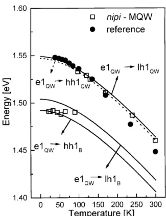
PLmeasurementsasafuntionoftemperature
how-ever, revealed dierenes in the optial properties
be-tween the doped and the referene samples. Fig. 5
showshow thePL peak energy hangedwith
temper-ature for both samples. The lines are theoretial
al-ulationstobedesribedbelow. Thereferenesample,
representedbysolidirles,behavesasshouldthe
opti-al transitionorrespondingtothersteletron-heavy
holetransitionintheQW,(e1
QW -hh1
QW
),asdepited
bythedashedlineinFig.5. Forthedopedsample,the
PLspetraasafuntionoftemperatureshowthatthere
andanotheroneathigherenergywhihisonly
observ-ableathighertemperatures. Attemperaturesabove90
K, this seond emissiondominatesthe spetra. In
or-der to better understand these results, alulationsof
thetemperaturedependenteletronistruture,within
thefullk.pHamiltonianmodelwereperformed,where
atriangularpotentialmodel(Fig. 4)wasusedto
simu-latetheloalizationofthearriersineahdopedlayer,
at their nominal densities. At low temperatures
(be-low 50 K), the experimental PL results are best
de-sribedbythetransitionbetweentherstQWeletron
andtherstbarrierheavy-holelevels(e1
QW -hh1
B );the
orrespondingholeprobabilitydensitiesofthedierent
energy levels involved are depited in Fig. 4. Suh
transition isspatially indiret. Attemperaturesabove
90 K, theexperimental resultsfollowthetemperature
behavior of the transition between the rst QW
ele-tron and rst barrier light hole levels (e1
QW -lh1
QW )
whih isdiret andonly afewmeV below the(e1
QW
-hh1
QW
)transition of the equivalent undoped sample,
as illustrated in Fig. 5. Thus, around 90 K the PL
emissionsuersatransitionfromindirettodiret.
Ex-perimental support for this hange in nature is found
in the resultsof PL asa funtion of exitation power
(P). The PL peak energy of the emissionat low
tem-peraturesisblue-shiftedwithinreasingP,whihisthe
standard behavior for spatially indiret transitions 13
,
while that oftheemission athigh temperaturesis
un-aetedbyP,indiatingadirettransition. SineatRT
the(e1
QW -lh1
QW
)transitiondominates,oneonludes
that the lh1
QW
level, in the half QW, is indeed
pop-ulated, demonstrating that holes are transferred from
thebarrierintotheQWs. Asaonsequene,partofthe
transferred holes,beinglosetotheinterfaeasshown
by the probabilitydensities in Fig. 4, are mostlikely
trappedbyinterfaestates.
IV Summary
GaAs/AlGaAs MQW strutures ontaining an nipi
delta-doped superlattie were investigated in order to
evaluatetheirpotentialforuseinhighperformane
am-plitude modulators based on the QCSE. First, it has
beenshownthatitispossibletoobtainsuitableC
delta-dopedAlGaAslayerseventhoughlittleexibilityisleft
in hoosing the growth onditions for a ontrolled C
doping of AlGaAslayers. Seond, ithasbeen
demon-strated that to ahieve the required balane between
thenandptypedopinglevelsoneshould onsiderthe
existene of hole traps at the interfaes whose
ou-panydependsontheQWn-dopinglevel. Finally,PL
measurements have shown that at RT only the
near-edge emission is observed, and it is only a few meV
belowthe fundamental transitionof anequivalent
un-dopedQW,notimpairing,inpriniple,theuseofsuh
Figure 5. PL peak energy as a funtion of temperature.
Solid irlesrepresent the measurements for the referene
samplewhosebehaviorfollowtheeletron-heavyhole
tran-sitions (e1
QW Q
hh1
QW
), represented by the dotted line.
Open squares are obtained from the measurements for a
MQW struture ontaining an nipi Æ-doping superlattie
(nipi-MQW).Athightemperatures(above90K)the
exper-imentalpointsarebestdesribedbythe(e1QW Q
lh1QW)
transition,whihinvolveseletronandholelevelsinsidethe
GaAs QW (diret transition). At low temperatures, the
experimentalpoints arebestdesribedby the (e1
QW Q
hh1B) transition fromthe rst eletronlevel inthe GaAs
QWtotherstheavyhole levelintheAlGaAsbarrier
(in-direttransition). At intermediarytemperatures (50-90K)
the experimental points are desribed by the (e1
QW Q
lh1B) indiret transition whih involves the QW eletron
andthebarrierlight-holelevels. Theprobabilitydensities
forthe holes, whihpartiipate intheemissions desribed
above,areshematiallyshowninFig. 4.
Aknowledgements
This work has been partially naned by CNPq,
CAPES,FAPERJ,ERICSSONandFAPESP.
Referenes
[1℄ M. K.Chin and W. S.C. Chang, IEEE J. Quantum
Eletron.29,2476 (1993).
[2℄ T.Ido, H.Sano,D. J.Moss e H.Inoue, J.Lightwave
Tehnol.14,2324(1996).
[4℄ W. Batty andD. W. E. Allsopp,Eletron.Lett., 29,
2066(1993).
[5℄ E.F.ShubertinSemiondutores andSemimetals 40,
hapter 1,edited by A. C. Gossard, AademiPress,
NewYork(1994).
[6℄ B. Yavih,P.L. Souza, M.P.Pires,A.B.Henriques,
andL.C.D.Gonalves,Semion.Si.andTehnol.12,
481(1997).
[7℄ P.L.SouzainInPandRelatedCompounds: Materials,
AppliationsandDevies, editedbyM. O.Manasreh,
hapter6,(2000).
[8℄ B. R. Davidson, L. Hart J. , R. C. Newman, T. B.
JoyeT.J.BulloughandC.C.Button,J.ofMat.Si.:
MaterialsinEletronis7,355(1996).
[9℄ T. Makimoto and N. Kobayashi,Jpn. J. Appl. Phys.
32,L1300(1993).
[10℄ N. Kobayashi, T. Makimoto and Y. Horikishi, Appl.
Phys.Lett.50,1435 (1987).
[11℄ M. B. Johnston, M. Gal, G. Li and C. Jagadish, J.
Appl.Phys.82,5748 (1997).
[12℄ F. Brunner, T. Bergunde, E. Rihter, P. Kurpas, S.
Gramlih, I. Rehenberg, S. Kraus, M. Ahouhe,
J. Wur and M. Weyers, Proeedings of the
EW-MOVPEVIII,Prague-1999.
[13℄ Y.Gong,J.Mo,H.Yu.L.WangandG.Xia,J.Crys.
Gr.209,43, (2000).
[14℄ G.E.Hoer,H.J.Hoer,N.Holonyak,Jr.andK.C.
Hsieh,J.Appl.Phys.72,5318(1992).
[15℄ P. Abraham, M. A. Garia Perez, T. Benyattou, G.
Guillot, M. Saolotti and X.Letartre, Semiondutor