Universidade do Minho
Escola de Ciências
João Miguel Peixoto Oliveira
outubro de 2017
Modelização de Espectros de Raios-X em Filmes
Finos
João Miguel Peixoto Oliveira
Modelização de Espectros de Raios-X em F
ilmes F
inos
Universidade do Minho
Escola de Ciências
João Miguel Peixoto Oliveira
outubro de 2017
Modelização de Espectros de Raios-X em Filmes
Finos
Trabalho realizado sob orientação do
Professor Doutor Bernardo Gonçalves Almeida
Dissertação de Mestrado
Mestrado em Física
Ramo de Física Aplicada
D E C L A R AT I O N
Nome: João Miguel Peixoto OliveiraEndereço electrónico: [email protected]
Telefone: (H) (+351) 253 321 371 · (M) (+351) 918 206 264 Número do Cartão de cidadão: 13 974 167
Título dissertação: Modelização de Espectros de Raios-X em Filmes Finos
Orientador: Professor Doutor Bernardo Gonçalves Almeida Ano de conclusão: 2017
Designação do Mestrado: Mestrado em Física - Ramo de Física Ap-licada
É AUTORIZADA A REPRODUÇÃO INTEGRAL DESTA TESE / TRABALHO APENAS PARA EFEITOS DE INVESTIGAÇÃO, ME-DIANTE DECLARAÇÃO ESCRITA DO INTERESSADO, QUE A TAL SE COMPROMETE.
Universidade do Minho, Outubro 2017
A B S T R A C T
Thin film multilayers are layered structures composed of several differ-ent materials and are commonly prepared for specifically envisaged ap-plications. X-ray diffraction is a nondestructive technique particularly suited for studying their structural properties. However, extracting structural parameters from X-ray diffraction, such as spacing between individual atomic planes, interlayer roughness or strain, requires mod-elling and fitting the X-ray diffraction spectra.
Here, we present a general kinematical model for wide angle X-ray diffraction of thin films that includes both the average atomic structure of the layers and structural disorder, for fitting the measured X-ray dif-fraction spectra. This model allows the extraction of composition (layer thicknesses), intralayer disorder and interfacial strain at the atomic scale that is assumed to be cumulative throughout the multilayer. In addition to the kinematical model, we also used an optical model for small angle X-ray reflectometry that allows us to obtain the composi-tion (layer thicknesses and electronic density) and interfacial roughness. Unlike simpler fits of X-ray diffractograms that use functions like Gaus-sian, Lorentzian, or pseudo-Voigt, this model allows a more complete and accurate determination of the structure parameters.
By fitting the measured profiles, it is possible to quantitatively de-termine both lattice constants and disorder parameters of a wide vari-ety of multilayers. The model was applied to the characterisation of La0.67Sr0.33MnO3\SrTiO3\Bi0.9La0.1FeO3 trilayer films as a function of the different relative layer compositions in these nanostructures.
R E S U M O
Os filmes finos multicamada são estruturas compostas por camadas de vários materiais diferentes e são normalmente preparadas para ap-licações específicas, pretendidas. A difração de raio-X é uma técnica não destrutiva particularmente adequada para estudar as suas propriedades estruturais. No entanto, extrair parâmetros estruturais da difração de raio-X, como o espaçamento entre planos atómicos individuais, rugosid-ade entrecamadas ou tensão, requer a modelização e ajuste de espectros de difração de raio-X.
Neste trabalho, apresentamos um modelo cinemático para ajustar os espectros de difração de raio-X medidos em altos ângulos, que inclui tanto a estrutura atómica média das camadas bem como a desordem estrutural. Este modelo permite extrair a composição (espessura das ca-madas), desordem intra camadas e interfacial, à escala atómica, que é assumida como sendo cumulativa ao longo da multicamada. Para além do modelo cinemático também usamos um modelo ótico aplicado a re-flectometria de raios-X (em baixos ângulos) que nos permite obter a composição (espessura e densidade eletrónica das camadas) e rugosid-ade interfacial. Ao contrário de ajustes mais simples de diffractogramas de raio-X que usam funções como Gaussiana, Lorentziana ou pseudo-Voigt, este modelo permite uma determinação mais completa e precisa dos parâmetros estruturais.
Ajustando os perfis medidos é possível determinar quantitativamente tanto as constantes de rede como os parâmetros de desordem para uma vasta gama de multicamadas. O modelo foi aplicado na caracterização de filmes com tricamadas de La0.67Sr0.33MnO3\SrTiO3\Bi0.9La0.1FeO3 em função das diferentes composições relativas das camadas nestas nanoestruturas.
C O N T E N T S
1 introduction 1 1.1 X-ray Diffraction 1 1.1.1 𝜃–2𝜃 Method 3 1.1.2 Radiation 4 1.1.3 Spacing Formulae 6 1.1.4 Models 6 1.2 Materials 71.2.1 Multiferroic Magnetoelectric Materials 7 1.2.2 Perovskite 10
1.2.3 Lanthanum Strontium Manganite 12 1.2.4 Strontium Titanate 13
1.2.5 Bismuth Lanthanum Ferrite 14 2 experiment 17
2.1 Pulsed Laser Deposition 17 2.1.1 Target Ablation 18
2.1.2 Vapour Plume Transport 19 2.1.3 Thin Film Growth 19
2.1.4 Advantages and Disadvantages 20 2.1.5 Lattice Mismatch 20
2.1.6 Deposition Setup 21 2.2 X-ray Measurement Setup 22 3 small-angle x-ray model 25
3.1 Refraction Index 26
3.2 Total External Reflection 27
3.3 X-Ray Reflectivity in Multilayers 28 3.4 Roughness 31
3.5 Fitting 31
4 wide-angle x-ray model 39 4.1 Ideal Model 41
4.2 Atomic Spacing Fluctuation 44
4.3 Lattice-Mismatched Incoherent Interface 54 4.4 Layers Thickness Fluctuation 56
4.5 Final Fitting Equation 62 4.6 Fitting 64
5 conclusion 75
5.1 Suggestion of Future Works 75 bibliography 77
L I S T O F F I G U R E S
Figure 1 Bragg diffraction of X-ray by a crystal lattice. 2 Figure 2 Schematic of an XRD measurement apparatus. 3 Figure 3 Scattering vector in an elastic XRD. 4
Figure 4 Relationship between multiferroic and magne-toelectric materials. 8
Figure 5 Hysteresis loops typical in ferroelectric, ferro-magnetic and magnetoelectric materials. 9 Figure 6 Multilayered structure of the studied thin films. 10 Figure 7 Perovskite’s cubic unit cell. 10
Figure 8 Common distorted perovskite structures. 11 Figure 9 Relation between orthorhombic and
pseudocu-bic lattices. 12
Figure 10 La0.67Sr0.33MnO3 unit cell. 13 Figure 11 SrTiO3 unit cell. 13
Figure 12 Bi0.9La0.1FeO3 unit cell. 14
Figure 13 Schematic of a pulsed laser deposition system. 17 Figure 14 Main steps of pulsed laser ablation. 18
Figure 15 Effects of lattice mismatch on the stress states of thin films. 21
Figure 16 Schematics of the plane of incidence in a strat-ified medium. 25
Figure 17 SAXS reflectivity spectra of a single-layered sample. 28 Figure 18 Wave vectors of the incident and reflected waves. 29 Figure 19 Fitted SAXS spectra of the BSL samples. 35
Figure 20 Comparison of the critical angle between the samples. 36
Figure 21 Types of multilayer structures the kinematic mod-els tries to model. 39
Figure 22 Representation of a multilayer structure. 40 Figure 23 The atomic planes are shifted due to disorder. 44 Figure 24 Error function erf(𝑥). 49
Figure 25 Effect of the variation of the WAXS model para-meters in the spectra. 65
Figure 26 Effect of variation of the interface spacing stand-ard deviation in the WAXS spectra. 66 Figure 27 WAXS diffractogram of a SrTiO3substrate. 69
Figure 28 Fitted WAXS spectra of the BSL samples. 71
L I S T O F TA B L E S
Table 1 Perovskite structure given the Goldschmidt’s tol-erance factor. 11
Table 2 Summary of the structural information of the used materials. 15
Table 3 Summary of the deposition parameters used to produce the studied BSL samples. 23 Table 4 Atomic form factor values of the atoms and
ma-terials used. 32
Table 5 Lattice parameters and atomic densities of the used materials. 33
Table 6 Summary of the obtained fit results for SAXS of the BSL samples. 37
Table 7 Structural parameter values of the BSL samples obtained by WAXS. 72
Table 8 Expected and obtained thicknesses for the lay-ers of the characterized BSL samples. 72
A C R O N Y M S
LSMO La0.67Sr0.33MnO3STO SrTiO3
BLFO Bi0.9La0.1FeO3
BSL La0.67Sr0.33MnO3\SrTiO3\Bi0.9La0.1FeO3 XRD X-ray diffraction
SAXS small-angle X-ray scattering WAXS wide-angle X-ray scattering PLD pulsed laser deposition PVD physical vapour deposition
1
I N T R O D U C T I O N
Heterostructures can give origin to physical phenomena that would be difficult or even impossible to achieve any other way. Many of these phenomena depend on the structural properties of the multilayers. As such, it is essential to have an accurate structural characterisation of the multilayers. Several techniques allow this type of characterisation, among them the X-ray diffraction (XRD) is well suited for this job. This technique not only provides an accurate structural characterisation of the individual layers at the atomic scale but it is also non-destructive, affordable and readily available.
The technique is important, but we also need a reliable model that describes the data to obtain the structural information. A simple ap-proach is to fit the XRD spectra with Gaussian, Lorentzian, or pseudo-Voigt functions to obtain the lattice parameters, grain size and strain information. However, to get a more detailed characterisation, we need a model that describes the structure. An optical model like the transfer-matrix method that resorts to Fresnel equations allow such character-isation. It takes into account phenomena like the total reflection and surface disorder. This method works particularly well in small-angle X-ray scattering (SAXS) to detect electronic density changes.
On the other hand, wide-angle X-ray scattering (WAXS) is sensible to the atomic spacing and requires a different model. Fullerton et al. [1] and Meng et al. [2] present a kinematic model to describe WAXS of superlattice structures. Their models assume an integer number of atomic planes and are limited to periodic bilayers. However, we want to study non-periodic multilayers. Thus, we developed a kinematic model to accommodate an arbitrary number of non-periodic layers with a real number of planes. We subsequently developed a suitable fitting software to perform the analyses of WAXS diffractograms with that model.
Here, we will describe and apply both models to analyse the structure of multilayer samples. These samples are composed of La0.67Sr0.33MnO3\ SrTiO3\Bi0.9La0.1FeO3. They combine multiferroic and multilayer prop-erties to produce a spin-filtering effect.
1.1 X-RAY DIFFRACTION
XRD is a nondestructive technique that employs radiation with a wavelength in the order of the interatomic distance and allows the structural char-acterisation of materials[3]. More specifically it permits the obtention
2 introduction
of structural information such as the type and parameters of a crystal lattice, preferred crystallographic orientations, the crystallinity of the material, and information about the crystallites like grain size, strain states, roughness, and several others.
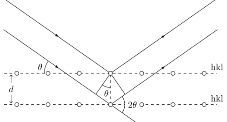
The X-ray radiation interferes with the lattice and is scattered. The interference can be constructive yielding maxima of intensity when the difference between travelled paths is an integer multiple (𝑛) of the in-cident wavelength 𝜆. For specular reflection of a monochromatic radi-ation (see fig. 1), the condition for constructive interference is given by Bragg’s Law[3]:
2𝑑 sin 𝜃 = 𝑛𝜆 (1)
, where 𝑑 is the distance between diffraction planes in a crystal lattice and 𝜃 is the angle of incidence. With specular reflection, the incid-ent and reflected angles are the same, which means the radiation is scattered by an angle of 2𝜃, known as scattering angle, see fig. 1.
hkl hkl 𝑑 2𝜃 𝜃 𝜃
Figure 1: Bragg diffraction of X-ray by a crystal lattice. Two identical X-ray beams are scattered by atoms from a crystal lattice. The scattered beams have a travelled distance difference between them of 2𝑑 sin 𝜃. Constructive interference occurs when this difference is equal to an integer multiple of the radiation wavelength.
It’s common to separate the XRD is two regions, small (2𝜃 typically below 10°) and wide angle (2𝜃 above 10°)[1], named small-angle X-ray scattering (SAXS) and wide-angle X-ray scattering (WAXS), respect-ively. The shape of the spectra in those regions is different and requires distinct analyses. The information provided by each region is also dif-ferent.
SAXS is sensitive to electronic density changes, interfaces and chem-ical modulation. Optchem-ical models provide reasonable descriptions for SAXS. These models can take into account the interfaces and the total reflection phenomenon. With them, we can determine the total thick-ness, associated with the Kiessig fringes[4], the period of superlattices, associated with the Bragg peaks and the interfacial and interdiffusion roughnesses.
1.1 x-ray diffraction 3
On the other hand, WAXS is sensitive to structural changes, namely changes in the distance between atomic planes, interlayer order, and chemical modulation. Unlike in SAXS, a kinematic model provides a reasonable description for WAXS.
Several techniques allow the structural characterisation of multilayer thin films, each with its advantages and disadvantages. Some benefits of XRD is that it is nondestructive[3]. Air does not absorb much the X-ray, so, a vacuum is not required. Low energy XRD is readily available, can be performed quickly and is relatively inexpensive. Diffraction can be done with the wave-vector in practically any orientation, allowing getting information on different nanostructure directions.
However, XRD also has its disadvantages. It requires a large enough sample and some structural order; therefore, small structures that are present only in trace amounts will often go undetected. In general, the heavier the atom, the stronger the interaction with the X-ray, as such, light elements can be difficult to detect.
1.1.1 𝜃–2𝜃 METHOD
The X-ray apparatus can use different measurement configurations, the most common is the 𝜃–2𝜃. In this configuration, the source of X-ray mains fixed, while the sample and detector are rotated by 𝜃 and 2𝜃, re-spectively. Moreover, the distance between the sample and source, and between the sample and detector remain constant during the measure-ment[3]. The basic X-ray optics for this type of setup are illustrated schematically fig. 2. Detector X-ra y Source 2𝜃 𝜃 Sample
Figure 2: Simplified schematic of an XRD measurement apparatus in a 𝜃–2𝜃 configuration. In this configuration, the sample and detector are rotated by 𝜃 and 2𝜃, respectively.
For an elastic scattering, the incident and scattered waves have the same wavelength, and consequently, the wave vectors have the same magnitude. In the case of specular reflection, both wave vectors make
4 introduction
the same angle 𝜃 with the surface. The scattering vector, in that case, follows Laue’s condition:[5, 6]
⃗
𝑞 = ⃗𝑘′− ⃗𝑘 (2)
, where ⃗𝑘 and ⃗𝑘′ are the incident and scattered wave vectors,
respect-ively. In this case, the scattering vector is always perpendicular to the surface[5], see fig. 3. Since the scattering vector is perpendicular to the surface, we scan the structure along the growth direction of the thin film[7]. ⃗𝑘 ⃗𝑘′ Sample Sample ⃗ 𝑞 − ⃗𝑘 𝜃 𝜃
Figure 3: Geometry of the scattering vector construction in an elastic X-ray
diffraction. The incident wave vector ⃗𝑘, reflected wave vector ⃗𝑘′and
the scattering vector ⃗𝑞= ⃗𝑘′− ⃗𝑘, that satisfies the Laue condition.
1.1.2 RADIATION
To perform XRD we need a source of X-ray radiation, the most common in small laboratories are X-ray tubes with a copper anode. These tubes emit non-monochromatic characteristic radiation with both a continu-ous spectrum through Bremsstrahlung and discrete emission peaks[3]. The most significant emission lines for copper tubes are the following, in the Siegbahn notation[3, 8–12]1:
CuK𝛼1 1.540 59Å
CuK𝛼2 1.544 42Å
CuK𝛽1,3 1.392 23Å
It is desirable to have a monochromatic radiation, because it would only produce a single diffraction per family of crystal planes, simpli-fying the analysis. Therefore, it is necessary to select one peak from the polychromatic radiation emitted by the tube; naturally the most
1 Other X-ray emissions for different elements can be found in the NIST X-Ray
Trans-ition Energies Database[13] or the Spectr-W3Database on Spectroscopic Properties
1.1 x-ray diffraction 5
intense is chosen. There are two ways to achieve this, with a monochro-mator or an appropriated filter placed before the detector[3]. With the use of one of them, it is possible to select the CuK𝛼 radiation, mitigat-ing the remainmitigat-ing emissions[11].
The CuK𝛼 radiation is composed by two peaks, the CuK𝛼2 having
half the intensity of CuK𝛼1. For simplicity, we will consider the
incid-ent radiation is monochromatic, with a wavelength that is the weighted average (CuK ̄𝛼) of the doublet, with the following wavelength and en-ergy[8, 11]:
CuK ̄𝛼 1.541 84Å 8.041 keV
The CuK𝛼 X-ray has a typical penetration depth of a few tens of micrometres in solid materials[15], which makes it a natural choice for the structural characterisation of thin films. However, if the thin film thickness is well below the depth penetrated by the X-ray, the signal from the thin films will be obscured by the signal from the substrate. The penetration depth is given by the absorption 𝜇 times the sine of the incident angle[15].
𝜏 = 𝜇 sin(𝜃) (3)
Note that the depth depends on the sine because the angle is defined between the surface and the incident beam, as shown in fig. 1. Since the depth is proportional to sin(𝜃), it is possible to control the measured depth to a certain extent. The less the substrate is penetrated, the better signal-to-noise ratio of the spectra, meaning that the spectra as less intensity from the substrate obscuring the thin film peaks. The peaks of the spectra present multiple orders at different angles, as such, we can select the lowest possible order that fully penetrates the film to obtain the best signal-to-noise ratio.
The absorption length is defined by Beer-Lambert law as when the beam flux drops to 1/𝑒 of its incident flux, and is given by:[15, 16]
𝜇 = 𝜆 4𝜋𝛽 = 1 2𝜆𝑟𝑒∑ 𝑎 𝜌𝑎𝑓𝑖 𝑎 (4) , where 𝑟𝑒 is the Lorentz classical electron radius (2.818 fm in SI units[16]),
𝜌𝑗,𝑎 the atomic density, 𝑓𝑖
𝑎 the imaginary atomic scattering factor for
each atom of 𝑎 in the layer 𝑗, and 𝛽 is the imaginary part of the ma-terial refraction index. The refraction index will be explored in more detail in section 3.1. Typically, the absorption length has values around 0.1 to 1 mm for 𝛽 of 10−7 to 10−8[16]. The penetration depth is also inversely proportional to the X-ray wavelength, the material’s density and absorption.
6 introduction
1.1.3 SPACING FORMULAE
The interplanar spacing 𝑑 depends on the lattice type. The relation between the unit cell parameters and the spacing for the cubic system is given by:[17]
1 𝑑2 =
ℎ2+ 𝑘2+ 𝑙2
𝑎2 (5)
, and for the hexagonal is 1 𝑑2 = 4 3 ℎ2+ ℎ𝑘 + 𝑘2 𝑎2 + 𝑙2 𝑐2 (6)
Note, that as referred in section 1.2.3, the perovskite derived struc-tures usually are described with a pseudocubic system because they have small deformations when compared with the perfectly cubic per-ovskite structure.
After determining the spacing of diffraction peaks, we can identify the crystallographic phases by comparing it with known values in the Powder Diffraction Files (PDF) from The International Centre for Dif-fraction Data (ICDD) powder difDif-fraction database.
1.1.4 MODELS
Each time the incident radiation crosses atomic planes, part of it is transmitted, and another is reflected. The reflected radiation can en-counter other planes, and the same effect will happen once again. The reflected radiation during its propagation can interfere with the remain-ing radiation. The dynamical theory of diffraction describes the effects of these multiple reflections and the interference they give rise[4, 18– 20].
Dynamic diffraction is important in perfect crystals but not so much in crystals with imperfections, since the imperfections do not permit a perfect periodicity in the whole crystal[3]. The radiation can be re-flected so many times that its mean travelled distance becomes higher than the coherence length. In that case, occurs an extinction of the observed beam at the crystal’s exit. In which case, the interference phe-nomena contribution should not be significant. In those situations, we can use a kinematic approximation. Although an approximation, it has the advantage of being simpler and better suited for the interpretation of the diffraction patterns used for structural determination.
In kinematic models, the scattered intensity maximum is propor-tional to the square of the number of atomic planes 𝑁 in the crys-tal. Thus, the scattered intensity may become unlimitedly large (𝐼→∞ when 𝑁→∞). By conservation of energy, this can not happen, else,
1.2 materials 7
the scattered beam intensity would be greater than the incident. The beam is absorbed as it penetrates the sample, progressively decreasing the effective incident intensity on the more interior planes, and con-sequently, decreasing the intensity scattered by them. However, the kinematic models assume the scattered photons result only from the collision with collision centres, in the middle of each layer. Thus, the kinematic model assumes the incident beam intensity is the same, in-dependently of the depth of the atomic planes to the sample’s surface. This is a limitation of the kinematic models, which makes them only applicable when the interaction of the X-ray beam with the sample is reduced, the number of atomic planes of the structure is small, or the grain size is small, so, that multiple internal reflections can be ignored. Typically, this occurs for nanoscopic materials in measurements done at wide angles, typically scattering angles 2𝜃>10°.
On the other hand, if the X-ray coherence length is relatively large in relation to the thickness of the sample, then the kinematic theory no longer is applicable. In those cases, it is necessary to resort to the dynamic theory to calculate the scattered intensity. This situation is verified, e.g., in epitaxial films or for X-ray measurements carried out at small angles. Based on the dynamic scattering formulation developed by Darwin[4, 19, 21–23] is possible to construct an optical formalism that permits the development of recursive formulae that are relatively simple to implement in fits of experimental spectra. They are valid provided that the electronic density of the nanostructures can be con-sidered continuous. These theories, allow the modelling of, namely, the refraction phenomena, total reflection and absorption, which are im-portant in the measurement regions of small angles.
1.2 MATERIALS
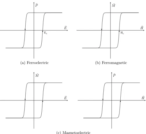
1.2.1 MULTIFERROIC MAGNETOELECTRIC MATERIALS Magnetic moment and electric dipole are usually mutually exclusive in crystals[24]. However, multiferroic materials breaks this principle of exclusion. These materials exhibit several ferroic orders simultaneously in the same phase, namely ferromagnetic, ferroelectric or ferroelastic orders[24–31]. As such, multiferroic materials, depending on the ferroic orders they possess, can have properties like magnetoelasticity, magne-toelectricity and piezoelectricity. In fig. 4 we can see the schematisation of the relation between multiferroics as well as the ferroic orders and their properties. The overlap between ferromagnetic and ferroelectric corresponds to multiferroic magnetoelectric materials.
Ferroelectric materials have a spontaneous electric polarisation that is stable and can be reversed by an external electric field and follows a
8 introduction
Magnetically
Polarizable PolarizableElectricaly
Multiferroic Ferromagntic Ferroelectric Magnetoelectric (a) Piezo electricit y d Magnetoelasticity Magneto electricit y 𝛼 S S XXMM XE XE E 𝜎 H P 𝜀 M (b)
Figure 4: Relationship between multiferroic and magnetoelectric materials. (a) Venn diagram with the relation between multiferroics and magne-toelectrics, illustrating the requirements to achieve both[32–35]. It should be noted that in this diagram we only consider the type of multiferroics that are simultaneously ferromagnetic and ferroelectric. (b) Schematisation of the possible cross-couplings in multiferroics.
Mechanical stress ⃗𝜎, electric field ⃗𝐸and magnetic field ⃗𝐻, and
elec-tric polarisation ⃗𝑃, magnetisation ⃗𝑀and strain ⃗𝜀. There remaining
letters represent the different coupling coefficients.[26, 28, 31–33, 35].
hysteresis loop[34], see fig. 5a. Ferromagnetic materials have a spontan-eous magnetisation that is stable and can be reversed by an external magnetic field and follows a hysteresis loop[34], see fig. 5b.
Magnetoelectric materials possess a coupling of between their electric and magnetic degrees of freedom. This coupling enables the induction of a magnetisation ⃗𝑀 through the application of an external electric field ⃗𝐸, but also the inverse, the appearance of electric polarisation ⃗𝑃 by applying a magnetic field ⃗𝐻[24, 28, 29, 31, 34, 36, 37]. This effect is observed in some, but not all, multiferroic materials that present simul-taneously ferroelectricity and a magnetic order, like ferromagnetism, as schematized by the Venn diagram in fig. 4. These materials follow ⃗𝐸- ⃗𝑀 or ⃗𝐻- ⃗𝑃hysteresis loops that look somewhat similar to the ferroelectric or ferromagnetic hysteresis loops[38], as seen in fig. 5c. Nevertheless, these properties are neither necessary nor sufficient for magnetoelectri-city[39]. Magnetoelectricity is an independent phenomenon from both ferroelectricity and ferromagneticity, but it is typical for this type of materials, emerging either directly or via strain[31, 34], and can only be large in ferroelectric or ferromagnetic materials[36]. The origin of the magnetoelectric coupling can be intrinsic to the material itself, or it can be the result of the combination of the properties of different materials[28].
Magnetoelectric multiferroics with their coupling between tric and ferromagnetic properties allow a magnetic control of ferroelec-tric domains or an elecferroelec-tric control of magnetic domains, which leads to new possibilities in the design of data storage devices[24, 31, 40–
1.2 materials 9 Ec ⃗ 𝐸 ⃗ 𝑃 (a) Ferroelectric Hc ⃗ 𝐻 ⃗ 𝑀 (b) Ferromagnetic ⃗ 𝐸 ⃗ 𝑀 ⃗ 𝐻 ⃗ 𝑃 (c) Magnetoelectric
Figure 5: Hysteresis loops typical in ferroelectric, ferromagnetic and
magneto-electric materials. (a) Hysteresis loop of ⃗𝑃 vs. ⃗𝐸typical of a
ferro-electric. (b) Hysteresis loop of ⃗𝑀vs. ⃗𝐻typical of a ferroemagnetic.
(c) Hysteresis loops that occur in ferroelectric materials with mag-nectoelectric properties.[24, 40]
42]. Some multiferroics can be ferroelectric and ferromagnetic, which provides an opportunity to encode information in four logic states, us-ing both electric polarisation and magnetisation[31, 43]. Bi0.9La0.1FeO3 is one of such materials[44].
The transport of information through electron spins, instead of charge, represents an important step to integrate both memory and logic in a single storage device[24, 41, 45, 46]. Spin-filters presents a way to create a spin-polarised electron current. A spin-filter is a device that filters electrons with spin unpolarised that tunnel between two ferromagnetic metallic layers through an insulator barrier. To achieve a spin-filtering effect the insulator acts as a barrier that is higher for a spin direction than the other giving different probabilities to tunnel depending on the electron’s spin[47, 48]. Currently, also exists an interest in imaging spin-filter techniques[49]. Multiferroics exhibit electric and magnetic orders simultaneously, making them promising spin-filter materials[43, 49].
10 introduction
1.2.2 PEROVSKITE
Although considerable research has been carried out to find multiferroic materials, only a few single phase materials present both multiferroic and magnetoelectric properties at room temperature[50–52]. Bismuth lanthanum ferrite (Bi0.9La0.1FeO3), commonly referred as BLFO, is one of the most promising magnetoelectric multiferroics at room temperat-ure.
In this work we studied trilayered thin film samples composed of a layer of BLFO followed by strontium titanate SrTiO3 (STO) and lanthanum strontium manganite La0.67Sr0.33MnO3 (LSMO) on top of
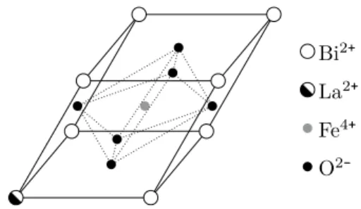
a STO substrate, has presented on fig. 6.
BLFO STO STO LSMO STO STO
Figure 6: Multilayered structure of the studied thin films.
The STO and LSMO were chosen not only for their properties but also because they share with the Bi0.9La0.1FeO3(BLFO) the same type of lattice structure and have similar lattice parameters. All the used materials have a perovskite crystalline structure, with chemical formula ABO3, where A is a divalent or trivalent metal and B is a trivalent or tetravalent metal. This crystalline structure is formed by a cubic lattice of cations A with both a body-centred cation B and face-centred oxygen ions. The unitary cell of the structure is depicted in fig. 7, as well as, the BO3 octahedron.
A2+
O
2-B4+
Figure 7: Perovskite’s cubic unit cell.
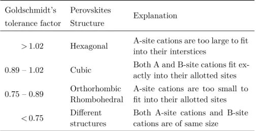
The stability and distortion of the perovskite crystalline structure depend on the ratio of the ionic radii. The Goldschmidt’s tolerance factor 𝑡[27, 53–56] is a dimensionless number used to describe this, and is given by:
𝑡 = √𝑟𝐴+ 𝑟𝑂
1.2 materials 11
, where 𝑟𝐴, 𝑟𝐵, and 𝑟𝑂 are respectively the radii of the A, B, and
the oxygen ions. A Goldschmidt’s tolerance factor of 1 means that the perovskite structure is cubic[54, 57]. The cubic perovskite structure is stable for Goldschmidt’s tolerance factors between 0.89 and 1.02[53, 58– 60]. When the factor is different, the cell becomes distorted and occurs rotations of the BO3 octahedron, given rise to non-cubic structures. In
table 1, we can see the correspondence between the Goldschmidt’s tol-erance factor and the type of perovskite crystalline structure. A factor between 0.75 and 1.00 is a necessary condition to form a perovskite, but it is not sufficient[61].
Table 1: Perovskite structure given the Goldschmidt’s tolerance factor[53, 58– 60].
Goldschmidt’s Perovskites Explanation tolerance factor Structure
> 1.02 Hexagonal A-site cations are too large to fitinto their interstices 0.89 – 1.02 Cubic Both A and B-site cations fit ex-actly into their allotted sites 0.75 – 0.89 OrthorhombicRhombohedral A-site cations are too small tofit into their allotted sites
< 0.75 Differentstructures Both A-site cations and B-sitecations are of same size The STO has a Goldschmidt’s tolerance factor of 1.00[53, 57, 60, 62], giving a cubic perovskite structure. Both the LSMO and BLFO on the other hand present a rhombohedral distortion[7, 44, 63, 64].
(a)
A2+
O
2-B4+
(b)
Figure 8: Common distorted perovskite structures. (a) Orthorhombic. (b)
Rhombohedral. ⃗𝑃is the electric polarization.
Due to changes in the B–O bonds, the octahedron is distorted leading to structural distortions. The displacement of B in the octahedron and rotations of the octahedron, due to variations in the B–O–B angle are also a common cause[65]. In proper multiferroics, the ferroelectricity emerges due to the classical stabilisation of off-centred ions that lead to
12 introduction
a macroscopic electric dipole[66]. Most of these compounds crystallise into a perovskite structure[51, 67]. Depending on the combination of the A and B cations, the perovskite can be an insulator, conductor or superconductor. It can present ferroelectric, ferromagnetic or even nonlinear optical behaviours[27].
A distorted perovskite, usually, does not change much from its cu-bic form, and as such, it is common to describe it using a pseudocucu-bic system instead of a orthorhombic one. The orthorhombic lattice para-meter 𝑎 is related to the pseudocubic parapara-meter 𝑎0 by the relation:
𝑎 =√2𝑎0 (8)
The relation between both lattices is visible in fig. 9.
𝑎0 𝑎 (a) 𝑎0 𝑎 (b)
Figure 9: Relation between orthorhombic and pseudocubic lattices. Or-thorhombic lattice viewed along the crystal’s c-axis direction, par-allel to the diagonals of the perovskite cube, i.e., [001] for the hexagonal system or [111] for the pesudocubic one.
The La0.67Sr0.33MnO3\SrTiO3\Bi0.9La0.1FeO3(BSL) samples are made
from perovskites. In this section, we present a brief description of the materials that compose the samples, by deposition order. We will review their structural and electromagnetic characteristics that are essential for the proposed applications and the XRD analysis we will perform. 1.2.3 LANTHANUM STRONTIUM MANGANITE
Lanthanum strontium manganite (LSMO), has the chemical formula La1-xSrxMnO3. Its crystalline structure depends on the doping level x. For x<0.2, the structure is orthorhombic, between 0.2<x<0.5 is rhom-bohedral and for x>0.5 becomes tetragonal, at room temperature, and monoclinic, at low temperatures (see fig. 10). The samples we studied have a doping level of 0.33, so it has a cubic perovskite structure with a rhombohedral distortion. The colossal magnetoresistive manganites perovskites have small distortions from the cubic structure, therefore, they are usually described according to a pseudocubic notation[7, 63]. At room temperature, the La0.67Sr0.33MnO3 crystal structure has the
1.2 materials 13
following parameters: a=5.5023 Å and c=13.3569 Å in the R ̄3c space group[68, 69], see table 2.
La2+
Mn4+
O
2-Sr2+
Figure 10: La0.67Sr0.33MnO3 unit cell.
La0.67Sr0.33MnO3 has a Curie temperature TC around 370 K[69]. Be-low this temperature, it acts as a conductor to electrons of one spin orientation, but as an insulator or semiconductor for electrons with spins of opposite directions[27, 70]. Also, below TC, the spins of its electrons are aligned ferromagnetically thanks to the double-exchange interaction caused by doping the LaMnO3 with Sr on the La-site[33].
In the doping range 0.2<x<0.4, the ground state of the LSMO is fer-romagnetic and is one of the perovskite manganites that shows the co-lossal magnetoresistance effect[63, 71]. The coco-lossal magnetoresistance in this material is a result of the competition between two magnetic interactions, the double exchange and the superexchange[33]. However, the properties of manganite thin film can be different from the bulk ma-terials mainly due to strain[7, 63]. At TCoccurs a phase transition from ferromagnetic to paramagnetic[69, 70]. Thus, at room temperature, it is ferromagnetic.
1.2.4 STRONTIUM TITANATE
Strontium titanate (STO), has the chemical formula SrTiO3. The STO has a cubic perovskite structure (see fig. 11), with a Goldschmidt’s tol-erance factor of 1.00[53, 57, 60, 62]. At room temperature, the SrTiO3 crystal structure has the following parameters: a = 3.905 Å in the Pm3m space group[60, 72], see table 2.
Sr2+
Ti4+
O
14 introduction
STO is a good insulator with an indirect band gap of 3.2 eV, at a temperature of 0 K. At room temperature, the STO has a large dielec-tric permittivity (300)[60].
It is a substrate well suited to grow oriented LSMO films, due to the similarity of its lattice parameters with the pseudocubic ones from LSMO (see table 2) that allow the growth of the films with a small mismatch strain.
1.2.5 BISMUTH LANTHANUM FERRITE
Bismuth lanthanum ferrite (BLFO), is a magnetoelectric multiferroic with the chemical formula Bi1-xLaxFeO3. The non-doped BiFeO3 at room temperature displays simultaneously large ferroelectric polarisa-tion and weak ferromagnetism, but only in thin film form[51, 52]. Dop-ing the crystal with La atoms to replace Bi atoms induces a “crys-tal pressure”[73]. A small La doping of x=0.1 stabilises the perovskite phase of the BiFeO3[74]. For this doping level, the BLFO has a
pseudoc-ubic perovskite structure with a rhombohedral phase, see fig. 12. At room temperature, the Bi0.9La0.1FeO3 crystal structure has the lattice parameters present in table 2.
Bi2+
Fe4+
O
2-La2+
Figure 12: Bi0.9La0.1FeO3 unit cell.
The “crystal pressure” induced by the La doping can transform the crystal’s structure from a rhombohedric phase into orthorhombic, see fig. 8[73]. Nevertheless, for a doping of x=0.1, the pressure is not high enough, and the structure remains rhombohedric. The BiFeO3 suffers from leakage currents, but the La doping also allows a reduction of the current density in six orders of magnitude. The BLFO remains ferro-magnetic at room temperature for x<0.3, losing it at higher temperat-ures[44].
Now that we discussed the structural and electromagnetic properties of the used materials, we present in table 2 a resume of their structural information that is relevant for the XRD analysis. In this table, we dis-play the hexagonal lattice parameters, 𝑎 and 𝑐, for the rhombohedric materials and their approximated pseudocubic, 𝑎0. From the
pseudoc-ubic lattice constants, we used Bragg’s Law from eq. (1) to estimate the scattering angles 2𝜃 for the (100) planes, taking into account the conditions used for the XRD measurements.
Table 2: Summary of the structural information of the used materials. The
lattice parameters 𝑎 and 𝑐 are in the hexagonal system, and the 𝑎0
in the pseudocubic system. Using Bragg’s Law and the pseudocubic lattice parameters we estimated the scattering angles 2𝜃 for the (100) planes.
Material Lattice 𝑎(Å) 𝑐(Å) 𝑎0(Å) 2𝜃100(degree) LSMO[68, 69] Rhombo. 5.502 13.357 3.891 22.856 STO[60, 72] Cubic — — 3.905 22.772 BLFO[44] Rhombo. 5.578 13.806 3.944 22.544
2
E X P E R I M E N T
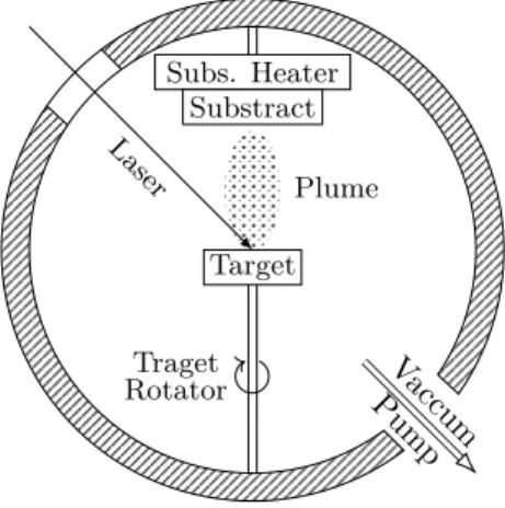
In this work, we studied multilayered thin films. These samples consist of three layers of perovskites with a few nanometers each consecutively deposited on top of a substrate. Exists a diverse multitude of techniques that allow the production of such samples. A subset of those techniques are the physical vapour deposition (PVD), that consists of the physical release of material from a target and its transport to a substrate. The studied samples were produced with a technique called pulsed laser deposition (PLD) that belongs to this group.
2.1 PULSED LASER DEPOSITION
PLD is a conceptually simple technique that uses a high power pulsed laser to eject material from a target. Figure 13 depicts a schematic diagram of its basic setup.
Laser Target Plume Subs. Heater Substract Traget
Rotator PumpVaccum
Figure 13: Schematic of a pulsed laser deposition system. A pulsed laser im-pinges on a target, removing material that deposits on a substrate, forming a thin film on its surface.
The deposition is effectuated inside a vacuum chamber that, if re-quired, can be filled with a background gas. Inside are several targets that are individually illuminated by a pulsed laser. The absorbed elec-tromagnetic energy is converted into electronic excitation that converts into thermal energy, leading to melting and vaporisation of the target. The ejected material forms a plasma plume, made by energetic neutral and ionic species, including polyatomic species[33]. The plume expands
18 experiment
perpendicular to the target surface, depositing on a substrate, form-ing a thin film. The process is then repeated until the layer has the required thickness, afterwards, each the target is changed to create the next layer, repeating the procedure till the samples have all the desired layers.
Now, we show a more in-depth review of the PVD process, which comprises three major steps that are be repeated several times during a deposition, they are[75, 76]:
1. Vaporisation of the target material 2. Transport of the formed vapour plume
3. Growth of a thin film on the substrate surface 2.1.1 TARGET ABLATION
The first step in the procedure is the extraction of the material that will be deposited. For that, a target is irradiated by a pulsed laser, leading to its melting and vaporisation. Figure 14 depicts the essentials of laser ablation[77].
(a) (b) Time (c) (d)
Figure 14: Main steps of pulsed laser ablation. (a) Initial absorption of the ra-diation (long arrows) and target melting (shaded area, short arrows indicate the motion of solid-liquid interface). (b) Heat flow spreads through the target, leading to its vaporisation and formation of a plume. (c) Vaporisation continuous and the radiation interacts with the plume, prompting the formation of a plasma. (d) Target cooling and solidification.[77]
During the whole process, a pulsed laser beam irradiates a target formed of the desired deposition material, or by a material that will later interact with a background gas to form the desired material. The laser pulse heats the surface, leading to the melting and vaporisation of the target. The ablation occurs due to subsurface heating induced either by the pulse or by the recoil pressure exerted by the material ablated in the initial part of the pulse[76]. As the vaporisation sets in, the latent heat acts as a cooling mechanism that leads the target’s subsurface to reach a higher temperature than the surface. Eventually, the continu-ous subsurface heating provokes an explosion of solid material on the surface, creating a highly forward-directed plasma plume[76, 78]. The
2.1 pulsed laser deposition 19
pulse eventually ends and, with it, the target heating, prompting the solidification of the material and recession of the melt front.
2.1.2 VAPOUR PLUME TRANSPORT
Heating the target prompts the formation of a plume formed by ejec-ted ions from all of the target elements, that roughly retains its stoi-chiometry[33]. The plume of ejecta is promptly irradiated by the laser pulse, absorbing radiation in the region where the density of charged particles is higher, that is, within a short distance from the bulk tar-get[79]. This absorption leads to the excitation and ionisation of species in the plume. Furthermore, it simultaneously reduces the intensity of the radiation reaching the target[77]. The plume initially propagates one-dimensionally [76, 77, 80, 81], however, beyond a distance com-parable to the dimensions of the laser spot becomes three-dimensional through adiabatic expansion due to the collision of the ejecta with the background gas and with itself, inside the plume[76]. The presence of a background gas slows and eventually stops the plume propagation after a few microseconds[82, 83].
2.1.3 THIN FILM GROWTH
In the final stage, the plume particles arrive and diffuse on the sub-strate, resulting in the creation of chemical bonds and growth of a thin film on its surface[84]. The morphology of the resulting film depends on several factors, namely, the kinetic energy of the arriving particles, the substrate temperature, the sticking probability, and the deposition rate[85]. Films deposited on substrates at room temperature are usually amorphous. However, their crystallinity can be improved if the sub-strate is at a higher temperature[77]. High subsub-strate temperatures and low deposition rates facilitate epitaxy, allowing for the diffusion of the adatoms on the substrate until they find equilibrium lattice sites[85]. As such, thin films deposited at low temperatures or high deposition rates tend to become amorphous. Another important aspect of the quality of the resulting thin film is the lattice mismatch between the substrate and the thin film. The properties and quality of the resulting film de-pend on several deposition factors, such as the choice of substrate and its temperature, the laser wavelength, pulse duration and intensity, and presence or not of background gas[7, 77].
20 experiment
2.1.4 ADVANTAGES AND DISADVANTAGES
Practically any material can be deposited by PVD[77]. Abundant re-ports have been made on the deposition of diverse materials, including multiferroics[77, 79, 83, 86–93]. It is a cost-effective preparation process that permits, for example, rapid prototyping for a wide range of mater-ials[33]. Furthermore, the deposition can create high-quality epitaxial films due to the high kinetic energy of the plume particles[94]. The con-gruent transfer of the bulk target material onto the film permits the preservation of its stoichiometry[33, 77, 87].
In addition to the high-quality samples produced by the technique, its implementation also presents advantages in relation to other depos-ition techniques. PVD does not require ultra-high vacuum[87] and the power source is outside of the chamber. Furthermore, the deposition of multilayers becomes straightforward with the use of multiple targets. The thickness of the layers can be controlled by tuning the material flux, the number of laser pulses or the deposition time. The thickness of the deposited layer is then given by:
𝑡ℎ𝑖𝑐𝑘𝑛𝑒𝑠𝑠 = 𝑓 × 𝑡𝑑𝑒𝑝 (9)
, where 𝑓 is the laser’s pulse frequency and 𝑡𝑑𝑒𝑝 is the deposition time.
Nevertheless, it also has disadvantages in relation to other PVD tech-niques, primarily two are of note. The first relates to the fact that due to the high directionality of the plume, the deposition of large ho-mogeneous films is hindered. The other is the possibility of exhibiting particles (droplets), due to explosive boiling of the target surface, with diameters in the order of the micrometre, which can meaningly affect the film properties[33]. Both of these makes the technique undesirable for industrial applications[28, 33]. However, their presence can be min-imized by using lower wavelengths and lower fluences to reduce the possibility of explosive boiling.
2.1.5 LATTICE MISMATCH
The interface between adjacent layers with different structures can present lattice mismatch. This mismatch induces stress in lattices of those layers, which influences their physical properties, e.g., transport and magnetic[33, 55, 95, 96]. The lattice mismatch between a layer 𝑖 and it neighbouring layer 𝑗 is defined as[27, 33]:
𝛿 = 2(𝑎𝑖− 𝑎𝑗) 𝑎𝑖+ 𝑎𝑗 ≈
𝑎𝑖− 𝑎𝑗
𝑎𝑗 (10)
, where 𝑎𝑖and 𝑎𝑗are layers in-plane lattice parameters. Positive 𝛿 values
indicate tensile (compressive) stress, whereas negative values produce compressive (tensile) stress in-plane (out-of-plane)[27], as schematized
2.1 pulsed laser deposition 21
in fig. 15. Epitaxial growth typically requires 𝛿<0.1[33]. This should not be a problem in the samples we will analyse as their materials have very close lattice constants and should produce 𝛿 well below 0.1. Although the lattice is deformed, the volume of its unit cell is maintained, as such, the tensile stress increases the lattice parameter perpendicular to the surface and decreases the in-plane lattice parameter, compressive stress has the opposite effect.
Tensile 𝛿 < 0
Compressive 𝛿 > 0
Figure 15: Effects of lattice mismatch on the stress states of thin films.
2.1.6 DEPOSITION SETUP
The PLD depositions were carried out in the pulsed laser deposition facilities of Centro de Física of Universidade do Minho (Gualtar).
Substrates of STO were placed inside a high vacuum chamber, on a resistive heater plate. The heater temperature Tsub was measured with
a thermocouple placed behind the plate and controlled by a Eurotherm 2116 PID Temperature Controller.
The substrate holder allows movement in a direction perpendicular to the target. With this, it is possible to adjust the distance between the target and the substrate dtar-sub. A target is placed in the centre of the vacuum chamber. During the deposition, the target rotates to allow a more uniform ablation. This, not only allows a higher utilisa-tion of the target materials but it also helps preserve the stoichiometry of the growing film[33]. A multitarget holder enables the deposition of multiple layers in the same deposition run by holding up to 4 inter-changeable targets.
Two pumps were used to achieve a high vacuum. An Alcatel Pascal 2010 I rotary pump allows a primary vacuum of 2 × 10⁻³mbar. After
that, an Alcatel ADP80 turbomolecular pump brings the pressure Pbase down to the desired 3 × 10⁻⁵mbar.
The chamber was filled with oxygen. This active gas will permit the formation of the oxides. With the introduction of oxygen, the pressure climbs to 0.8 mbar. A needle valve controlled the oxygen flux. While in a rough vacuum, the oxygen pressure was measured with an AML PGC1 Pirani gauge and with a KS 943 cold cathode Penning gauge during high vacuum.
The ablation of the target was carried out with a Lambda Physik® LPXpro™ 210 pulsed excimer KrF laser with a wavelength of 248 nm and a pulse duration of 25 ns. Each pulse carried an energy Elaser of
22 experiment
either 250 mJ or 450 mJ, depending on the sample. For each material, a pulse frequency 𝑓 was set. The laser beam irradiates the target at an angle of 45° with its surface.
The described procedure has carried out to produce five multilayered thin film samples with the structure illustrated in fig. 6. A summary of the deposition parameters for the different samples is displayed in the table 3, on the next page. The table 3 also has the expected thickness of each layer. The expected thicknesses were obtained empirically. We assumed a linear deposition rate and calibrated the deposition rates for samples previously produced with the thickness measured. The depos-ition rates for the used materials and deposdepos-ition setup are the following: LSMO 1/9 nm min−1Hz−1
STO 1/2 nm min−1Hz−1
BLFO 1/3 nm min−1Hz−1
2.2 X-RAY MEASUREMENT SETUP
The XRD measurements were carried out at Universidade do Minho (Gualtar). A 𝜃–2𝜃 geometry configuration has used for the XRD meas-urements. A copper tube was used, as the source of X-ray. With a monochromator we selected the CuK𝛼 emissions, giving an incident ra-diation approximately monochromatic with a wavelength of 1.540 59 Å. A scintillation detector was used to give a count of the diffracted radi-ation.
2.2 x -r ay m ea su r em en t se t u p 23
Table 3: Summary of the deposition parameters used to produce the studied BSL samples.
Sample Layer Elaser Beamsplitter Pbase Gas Pdep Tsub dtar-sub f tdep thickness
(mJ) (10−5mbar) (mbar) (∘C) (cm) (Hz) (min) (nm)
LSMO 450 50% 3.00 O2 0.8 700 5 3 30 10 BSL 5 STO 450 50% 3.00 O2 0.8 720 5 5 2.191 5 BLFO 450 50% 3.00 O2 0.8 700 5 3 5 5 LSMO 450/2501 50%/99%1 3.00 O 2 0.8 700 5.5 6 30/301 20 BSL 8 STO 450/2501 50%/99%1 3.00 O 2 0.8 720 5.5 5 1/21 5 BLFO 250 50%/99%1 3.00 O 2 0.8 700 5.5 6 40 80 LSMO 250 99% 3.00 O2 0.8 700 5.5 6 30 20 BSL 9 STO 250 99% 3.00 O2 0.8 720 5.5 5 3 7.5 BLFO 250 99% 3.00 O2 0.8 700 5.5 6 10 20 LSMO 250 99% 3.00 O2 0.8 700 5.5 6 30 20 BSL 10 STO 250 99% 3.00 O2 0.8 720 5.5 5 6 15 BLFO 250 99% 3.00 O2 0.8 700 5.5 6 20 40 LSMO 250 99% 3.00 O2 0.8 700 5.5 6 30 20 BSL 11 STO 250 99% 3.00 O2 0.8 720 5.5 5 9 22.5 BLFO 250 99% 3.00 O2 0.8 700 5.5 6 20 40
3
S M A L L - A N G L E X - R AY M O D E L
The small-angle X-ray scattering (SAXS) is a useful XRD technique to study the structure of thin films and multilayered samples. It is particularly helpful to determine structural information, namely the thickness of individual layers, the spacing between diffraction planes and the roughness, of interfaces and surfaces[16, 21, 97].
This type of XRD measurement deals with small angles, typically with scattering angles 2𝜃 below 10°[1]. Kinematic models are not well suited to describe such small angles, for instance, they do not predict total reflection, etc. Optical models are more appropriate for this task. These models assume the samples are composed of media with con-tinuous electronic densities and calculate the reflection and refraction at each interface. These media are described by refractive indices, and the knowledge of these is enough to predict what happens at the inter-faces[1, 16].
In this chapter, we present a general optical formalism to calculate the reflectivity of rough surfaces and interfaces of multilayers in func-tion of the radiafunc-tion’s incident angle 𝜃, which is valid for SAXS. The formulation will be based on the multilayer structure schematized in fig. 16. Air Layer 1 Layer 2 ⋯ Layer N Substrate Substrate 0 𝑧 𝑍𝑁 𝑍𝑁−1 𝑍2 𝑍1 𝑍0
Figure 16: Schematics of the plane of incidence in a stratified medium that will be described by the SAXS model. The system is composed of 𝑁+2 layers. Air is labelled layer 0, and layers of the stratified medium have labels 1≤𝑗≤𝑁. We will measure the travelled distance 𝑧 from the substrate interface.
This multilayered system is composed of 𝑁+2 layers with indices 𝑗, each layer is treated as a continuous medium with refraction index 𝑛𝑗.
If the penetration depth is smaller than the thickness of the sample, we will deal with 𝑁+1 interfaces that separate pairs of adjacent layers
26 small-angle x-ray model
with distinct refractive indices. The depth 𝑍𝑗 marks the interface the
layers 𝑗 and 𝑗 + 1. The layer with index 0 corresponds to the incident propagation medium, usually air, and the layer 𝑁+1 is the substrate. We presume the penetration depth is smaller than the thickness of the sample including the substrate, and as such, we will not consider the reflection that could occur in the interface Substrate/Air.
3.1 REFRACTION INDEX
Photoabsorption and coherent scattering are the two primary interac-tions with matter in low energy XRD. These processes are accurately de-scribed by the complex atomic scattering factor, 𝑓=𝑓𝑟+𝑖𝑓𝑖. The atomic
scattering factor is a measure of the scattering amplitude of a wave by an atom. This factor needs to be multiplied by the scattering amp-litude of a single free electron to yield the total ampamp-litude coherently scattered of an atom[98].
For photon energies above 50 eV, we can accurately describe the in-teraction with the X-ray if we consider the crystal as a collection of independent atoms. We will deal with CuK ̄𝛼 radiation with 8.041 keV, so, well within this regime. Thus, the total scattered amplitude is the sum of the amplitudes scattered by the individual atoms[98].
The interaction of X-ray with matter can be described by optical constants like the complex refraction index. This index is important for a quantitative understanding of the interaction between the X-ray and the materials. Each layer of the multilayer system is characterised by a complex refraction index 𝑛𝑗, in general, the refraction index of
matter for X-ray radiation is given by:[6, 16, 97, 98]
𝑛𝑗= 1 − 𝛿𝑗− 𝑖𝛽𝑗 (11)
, where the real and imaginary components, 𝛿 and 𝛽, describe the dis-persive and absorptive aspects of the wave-matter interaction. These two parameters depend on the type of radiation. The classical model of an elastically bound electron yields these parameters for the X-ray radiation,[6, 16, 97, 98]
𝑛𝑗= 1 − 𝜆
2𝑟 𝑒
2𝜋 ∑𝑎 𝜌𝑗,𝑎𝑓𝑗,𝑎 (12)
, where 𝑟𝑒 is the Lorentz classical electron radius with 2.818 fm[16],
𝜆 the incident radiation wavelength, 𝜌𝑗,𝑎 the atomic density (either in unit cells or atoms per volume unit) and 𝑓𝑗,𝑎 the complex atomic
scattering factor for each atom of type 𝑎 in the layer 𝑗. Photoabsorption determines the atomic form factor as a function of energy, a list of these
3.2 total external reflection 27
values can be found in tables, like the ones given by Henke et al. [98]. The 𝛼 and 𝛽 coefficients are defined as:[98]
𝛼 = 𝜆 2𝑟 𝑒 2𝜋 ∑𝑎 𝜌𝑗,𝑎𝑓𝑟𝑗,𝑎 (13) 𝛽 =𝜆 2𝑟 𝑒 2𝜋 ∑𝑎 𝜌𝑗,𝑎𝑓𝑖𝑗,𝑎 (14)
, where the difference is that the 𝛼 depends on the real part of the atomic form factor and 𝛽 depends on the imaginary part. The real component can also be defined as:[16]
𝛿𝑗= 𝜆
2𝑟 𝑒
2𝜋 𝜌𝑒,𝑗 (15)
, where 𝜌𝑒,𝑗 is the electronic density of layer 𝑗. Which means, that for
a fixed wavelength, the refraction index’s real part is proportional to the materials electronic density.
3.2 TOTAL EXTERNAL REFLECTION
Since the refraction index in the X-ray is slightly less than 1, the in-cident radiation impinged on a flat surface can suffer total external reflection[16]. Total external reflection is observed when the incident radiation is below a certain angle, that we will call critical angle 𝜃𝑐.
The critical angle determined by the Snell–Descartes’ Law for radi-ation that comes from a medium with refraction index close to 1, like air, is given by1:[16, 99]
cos 𝜃𝑐= 𝑛𝑗= 1 − 𝛿𝑗 (16) For the typical X-ray wavelengths, 𝛿 is small enough that we can safely use the small angle approximation for the cosine (cos 𝜃≈1−𝜃2/2),
with it, the critical angle can be approximated to:[16, 21, 99]
𝜃𝑐 ≈ √2𝛿𝑗 (17)
We rewrite it using eqs. (12) and (15), showing it proportionality to the materials electronic density,
𝜃𝑐 ≈ 𝜆√ 𝑟𝑒∑ 𝑎 𝜌𝑗,𝑎𝑓𝑗,𝑎 𝜋 = 𝜆√ 𝑟𝑒𝜌𝑒,𝑗 𝜋 (18)
As can be seen in fig. 17, because the X-ray is totally reflected, we observe a plateau of maximum reflectivity for angles below 𝜃𝑐. Total
external reflection in X-ray, is observed at incident angles with typical values 2𝜃<1.0°.
1 Note that eq. (16) is presented with cosine because the angle is defined between the surface and the incident beam, as defined in fig. 1.
28 small-angle x-ray model 0 0.2 0.4 0.6 0.8 1 𝜃𝑐 2𝜃(degrees) log Reflectivit y
Figure 17: SAXS reflectivity spectra of a single thin film layered sample of
GdMnO3/MgO. The dashed line marks the critical angle 𝜃𝑐, and
the vertical arrows indicate the Kiessig fringes.
The X-ray beam is fully reflected from the surface below the critical angle. However, an evanescent wave penetrates a short distance of the thin film. X-ray techniques like the grazing-incidence small-angle X-ray scattering (GISAXS) can exploit this evanescent wave to probe the thin film surface.
3.3 X-RAY REFLECTIVITY IN MULTILAYERS
The SAXS spectra are characterised by a rapid decrease of the re-flectivity for angles above the critical angle. This decreasing rere-flectivity can be modulated by an oscillatory behaviour that produces fringes called Kiessig fringes. Figure 17 gives an example of a SAXS spectrum that displays this type of behaviour. These modulations occur in mul-tilayered systems with layers that have a finite thickness in the order of magnitude of the incident radiation wavelength. In those cases, the ra-diation will undergo multiple internal reflections that interfere between themselves, given rise to the observed fringes[16, 21]. The angular spa-cing between Kiessig fringes is inversely proportional to the total film thickness[16]. Due to the relation between these fringes and the layers thicknesses, the roughness in the interfaces surfaces will destroy the co-herence and reduce, or even eliminate the fringes. So, well-defined and visible fringes are an indication of a film with sharp interfaces[100].
The radiation is reflected and transmitted on each interface between layers of different refraction indices, and consequently different elec-tronic densities. To describe the reflectivity and transmissivity in a
3.3 x-ray reflectivity in multilayers 29
multilayer system we need to take into account the multiple internal reflections that happen. Abeles’ matrix method provides a way to de-scribe propagation of radiation through different stratified media. In this approach, the refraction matrix 𝑅𝑗describes the refraction between
two media, and is defined as:[16, 101] 𝑅𝑗= [𝑝𝑗 𝑚𝑗
𝑚𝑗 𝑝𝑗] (19)
, with coefficients 𝑝𝑗 and 𝑚𝑗 that characterise the relation between the
magnitude of the electric fields in the media 𝑗 and 𝑗+1, they are defined as:[16]
𝑝𝑗= 𝑘𝑗,𝑧+ 𝑘𝑗+1,𝑧
2𝑘𝑗,𝑧 (20)
𝑚𝑗= 𝑘𝑗,𝑧− 𝑘𝑗+1,𝑧
2𝑘𝑗,𝑧 (21)
The wave vector 𝑘𝑗 is defined as shown in fig. 18.
𝑥 𝑧 ⃗𝑘𝑗 𝜃𝑗 ⃗𝑘 𝑗,𝑥 ⃗𝑘𝑗,𝑧 ⃗𝑘′ 𝑗 𝜃′ 𝑗
Figure 18: Wave vectors of the incident ⃗𝑘𝑗and diffracted ⃗𝑘′𝑗waves in a layer
𝑗. They are polarised along the y-axis and travel in the 𝑥𝑂𝑧 plane
of incidence.
The components of the wave vector of the incident wave are:
𝑘𝑗,𝑥 = 𝑘𝑗cos 𝜃𝑗 (22)
𝑘𝑗,𝑧 = −𝑘𝑗sin 𝜃𝑗= −√𝑘2
𝑗− 𝑘2𝑗,𝑥 = −√𝑘2𝑗− 𝑘2𝑗cos2𝜃𝑗 (23)
Using the dependence between the wavenumber and the refraction index, we can rewrite the normal component.
𝑘𝑗,𝑧 = −2𝜋
𝜆 𝑛𝑗√1 − cos2𝜃𝑗 (24) SAXS deals with small angles, as such, we can use the small angle approximation for the cosine.
𝑘𝑗,𝑧 ≈ −2𝜋 𝜆 𝑛𝑗√𝜃 2 𝑗− 𝜃4 𝑗 4 (25)
30 small-angle x-ray model
The angles are small enough that the 𝜃2
𝑗 will dominate the term 𝜃4𝑗/4.
𝑘𝑗,𝑧≈ −2𝜋
𝜆 𝜃𝑗𝑛𝑗 (26)
, replacing the refraction index, defined in eq. (12), 𝑘𝑗,𝑧= −2𝜋 𝜆 𝜃𝑗[1 − 𝜆2𝑟 𝑒 2𝜋 ∑𝑎 𝜌𝑗,𝑎𝑓𝑗,𝑎] (27) = [𝜆𝑟𝑒∑ 𝑎 𝜌𝑗,𝑎𝑓𝑗,𝑎−2𝜋 𝜆 ]𝜃𝑗 (28)
The electric field amplitude oscillates periodically along the radiation travel, possessing a dependence with the travelled time. The translation matrix 𝑇𝑗 describes this dependence, and is defined as:
𝑇𝑗= [𝑒
−𝑖𝑘𝑗𝑡𝑗 0
0 𝑒+𝑖𝑘𝑗𝑡
] (29)
, where 𝑡𝑗 is the thickness of the layer 𝑗, and is defined as:
𝑡𝑗= 𝑍𝑗− 𝑍𝑗−1 (30)
, where 𝑍𝑗 is the position of the interface between the layers 𝑗 and 𝑗+1,
as displayed in fig. 16.
The product of all the refraction and translation matrices of the entire system is the transfer matrix 𝑀,
𝑀 = [
𝑁−1
∏
𝑗=0
𝑅𝑗𝑇𝑗]𝑅𝑁 (31)
The reflection coefficient 𝑟 is the ratio between the reflected and incident electric fields on an interface. Although the X-rays penetration depends on the type of material, it is typically in the order of the micrometer[3, 15, 16], see section 1.1.2, well below the thickness of the typical substrates. Therefore, we assume there is no reflection back from the substrate. In that case, the reflection coefficient is:[16]
𝑟 = 𝑀12
𝑀22 (32)
In a SAXS experiment we measure the Fresnel reflectivity,
𝑅 = |𝑟|2 (33)
, which is a real number, unlike the complex reflection coefficient. The reflectivity loses the phase information given by the reflection coeffi-cient.
3.4 roughness 31
3.4 ROUGHNESS
Generally, interfaces are not perfect, they have a certain roughness and thickness. The roughness of the top layer is of particular importance to describe how fast the exponential decay above the critical angle occurs. To take into account the reduction in reflectivity caused by the interface roughness, the reflection coefficients from eq. (32) can be multiplied by the Debye-Waller-type factor 𝑆𝑗, defined as:[16]
𝑆𝑗= 𝑟 𝑟𝑜𝑢𝑔ℎ 𝑗 𝑟𝑓𝑙𝑎𝑡𝑗 = 𝑒 −𝑞2 𝑗𝜎2𝑗+1/2 (34) , where 𝜎2
𝑗 is the mean square height on the interface roughness, and
𝑞𝑗it the scattering vector on layer 𝑗. The scattering vector in a layer is given by:
𝑞𝑗= 4𝜋𝑛𝑗
𝜆 𝑠𝑖𝑛(𝜃) (35)
, with refraction index 𝑛𝑗of that layer. We should note that the SAXS
spectra are sensitive to the dimension of the overall roughness, inde-pendent of its nature[1].
For a multilayer with imperfect interfaces or surfaces, the experiment-ally measured reflectivity can be fitted by the eq. (33), with the reflec-tion coefficient for that structure determined by eq. (32) and adjusted by eq. (35) to take into account interface roughness. To perform the fitting, we can resort to an optimisation algorithm like the Levenberg-Marquardt algorithm[102, 103].
In summary, for a SAXS reflectivity spectrum, the presented model obtained with the Abeles’ matrix method allows the determination of the density and thickness of each layer and the mean height of the in-terfaces. The critical angle is related to the density of the constituent materials. The reflectivity is modulated, producing fringes. The amp-litude of these fringes depends on the roughness of the layers, interface quality and density variations. Furthermore, the separation between fringes is inversely related to the layer thickness[15].
3.5 FITTING
In this section, we will use the former model to analyse the SAXS spectra of our BSL samples. For that, we resorted to the aid of the solver SimulReflec 1.75[104] that implements the described model.
To determine the normal component of the wave vector, we need to know the density and atomic form factor of the materials that consti-tute the sample. We will start by determining the atomic form factors.
32 small-angle x-ray model
The atomic form factor depends on the incident energy and scatter-ing angle. However, it is independent of the scatterscatter-ing angle if the wavelengths are long compared to the atomic dimension (which they are not) or for small scattering angles[98]. Thus, we will consider the atomic form factor are constant in our analysis of the SAXS spectra. The XRD measurements were carried out with a copper tube source that emits radiation with a wavelength of 1.5406 Å, that we will con-sider as monochromatic for the fits. This wavelength has a correspond-ing energy of 8047.8 eV, obtained by the Planck-Einstein relation,
𝐸 = ℎ𝑐
𝜆 (36)
, for a value of ℎ𝑐 of 1.2398 × 10⁵eVÅ−1[105]. Henke et al. [98] provides
tables of atomic form factors for a vast selection of atoms and energies obtained through photoabsorption. However, this list does not contain the values for the energy we are dealing. Therefore, we did a linear interpolation using the two closest energies provided to obtain the de-sired values for our incident energy. The obtained values are presented in table 4. We calculated the form factors for the materials involved: LSMO, STO and BLFO. To do this, we calculated the values for the average unit cells of these materials, and the determined values are dis-played in the same table 4.
Table 4: Complex atomic form factor values of the atoms and materials used in the BSL samples. Atom 𝑓𝑟 𝑓𝑖 La 55.6747 9.7817 Sr 37.6425 1.8479 Mn 24.4563 2.8363 O 8.0524 0.0338 Ti 22.2421 1.8711 Bi 79.3175 9.3118 Fe 24.8476 3.2131 LSMO 98.3376 10.1012 STO 84.0418 3.8204 BLFO 125.9580 12.6733
As seen in section 1.2.2, STO presents an almost perfect cubic per-ovskite lattice. On the other hand, the LSMO and BLFO have rhom-bohedric perovskite lattices. These rhomrhom-bohedric perovskites usually have a small deviation from the perfect cubic perovskite, and as such, are treated as pseudocubic[7, 63]. Taking into account this, we used the pseudocubic approximation for those two materials. Thus, we determ-ined the unit cell volume as if it were cubic with the lattice parameters


![Figure 4: Relationship between multiferroic and magnetoelectric materials. (a) Venn diagram with the relation between multiferroics and magne-toelectrics, illustrating the requirements to achieve both[32–35]](https://thumb-eu.123doks.com/thumbv2/123dok_br/17297666.790739/19.892.263.740.111.343/relationship-multiferroic-magnetoelectric-materials-multiferroics-toelectrics-illustrating-requirements.webp)
![Figure 9: Relation between orthorhombic and pseudocubic lattices. Or- Or-thorhombic lattice viewed along the crystal’s c-axis direction, par-allel to the diagonals of the perovskite cube, i.e., [001] for the hexagonal system or [111] for the pesudocubic o](https://thumb-eu.123doks.com/thumbv2/123dok_br/17297666.790739/23.892.307.686.386.587/relation-orthorhombic-pseudocubic-thorhombic-direction-diagonals-perovskite-pesudocubic.webp)