Abstract—The main purpose of this paper is introducing a new method based on the transmission line approach for designing FSS-backed reflecarray antennas. For this reason a dual band reflectarray antenna is designed. This antenna contains a conventional single layer RA and a FSS backed double layer RA with 54% and 50% efficiency operating at X band and K band, respectively. A double layer FSS is used between RAs to isolate them. K band cell element is designed and analyzed using transmission line method and consideration of equivalent circuit for elements of each layer. Then the results obtained using this technique is compared to those found by CST and ADS. The comparison shows a good agreement. Jerusalem cross dipole with variable size is employed as radiation element in both bands. The most important properties of our suggested array are low cross polarization and high efficiency.
Index Terms— Reflectarray Antenna (RA), Frequency Selective Surface
(FSS), Transmission Line Method, Dual Band Antenna.
I. INTRODUCTION
Today, reflectarray antennas (RAs) are utilized in many applications because of their numerous
advantages. These antennas consist of reflective elements etched on a flat surface and a prime feeding
antenna illuminates these elements. Each reflective element introduces a pre-adjusted phase shift to
produce a constant phase front.
The most drawback of RAs is their narrow bandwidth. To overcome this disadvantage several
multiband and broadband antennas have been used to increase the band width [1-9]. Multi band
antennas can be implemented in single layer or multilayer configuration [1-9]. The former is used
when frequency are close and the latter used for wide frequency applications. An efficient technique
to design multilayer, multiband configuration is using FSS between reflective layers as band isolator,
which has been suggested in [1]. Also, in [2] a dual band X/Ku RA is implemented by this method.
In this study an analytical method is investigated to design FSS-backed RAs for the first time. So, a
lot of optimization methods in MATLAB can be utilized to optimize FSS parameters for better
performance. In this proposed method equivalent LC circuit is considered for each layer and with the
use of transmission line theory the impedance of whole structure is calculated. Also, transmission and
reflection coefficients are obtained. Using this analytical method a FSS-backed dual band, dual
ANALYTICAL METHOD FOR DESIGNING
FSS-BACKED REFLECTARRAY
ANTENNA USING TRANSMISSION LINE
APPROACH
Iman Derafshi, Nader Komjani and Ensiyeh Ghasemi-Mizuji
mentioned in [10]. This cascade configuration is composed of two arrays: a single layer conventional
X band array and a double layer FSS-backed K band array.
The proposed antenna shows a remarkable performance at both X and K bands (10.4-11.4 GHz and
20- 22.1 GHz) with efficiency of around 50% and 54%, respectively. The FSS placed between two
arrays acts as ground plane in K band and has transmission property at X band. Also, this applied FSS
layer creates isolation and reduces mutual coupling between the two proposed frequency bands.
Because of utilizing polarization insensitive unit cell, the designed antenna has similar operation for
both polarization and has a very low cross polarization.
II. DEVELOPMENT OF THE PROPOSED ANTENNA
As mentioned previously FSS-backed configuration is a suitable choice when operation bands are
apart. In this technique the upper band FSS-backed RA is located on top of the lower band
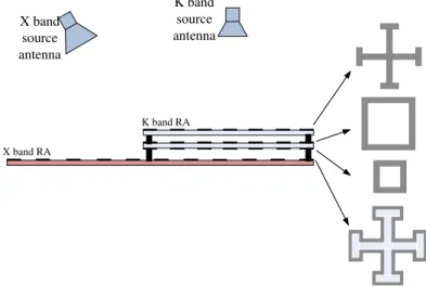
metal-backed RA. The schematic diagram of this configuration is shown in figure 1. Also, The prototype of
the antenna and cell element of each layer are specified in figure 1.
X band RA
K band RA
X band source antenna
K band source antenna
Fig. 1. Schematic of the proposed antenna.
The parameters of FSS-backed antenna are adjusted in order to reflects incident waves at k band
(20-22 GHz). and transmits them at X band (10.4-11.4 GHz). Using double layer FSS element gives
more degrees of freedom for optimizing parameters to have broadband FSS with mentioned
properties. Furthermore, using FSS physical and electrical isolation is achieved, additionally as it can
be understand from [11] as larger space between layers results in lower mutual coupling so the mutual
coupling between the RAs is decreased by placing FSS between them. In this article a double layer
FSS is utilized as band isolator which gives more degrees of freedom for optimization. For studying
dual band operation, at first step each antenna is simulated using CST software, separately. In the next
step all the structure (contain both X and K band antennas) is simulated to confirm suitable
III. OBTAINING K BAND RA PARAMETERS WITH USE OF TRANSMISSION LINE METHOD
A frequency selective surface consists of an array of periodic structures that used to control
incident wave in different ways such as filtering, isolating and changing phase and amplitude. As it
noted previously, the insertion of FSS between RAs reduces the mutual coupling between layers and
improve their isolation. If the layers have enough physical distance and the dielectric constant of the
substrate is small enough, mutual coupling can be ignored and RA layers have little effect on each
other and they can be designed and analyzed separately. In this section new method is suggested to
design and analyze FSS-backed unit cell.
K band unit cell is depicted in figure 2.a. In this unit cell, the Jerusalem cross dipole is used as
phasing element and the phase shift is compensated by variation of ld (Fig.2.b). This reflective layer is
located on top of the FSS layer with 2mm spacer (Fig.2.c and d). Rohacell foam (er=1.05, tan
d=0.0003) can be used as spacer to keep antenna layers together [14]. An array of square rings is
etched on both sides of lower substrate to operate as FSS. All of the substrates are 32-mil RO-4003.
The equivalent circuit of this unit cell is presented in figure 2.f. In figure 2.f η0 and ηd are the free
space and the substrate impedances, respectively.
η0 ηd η0 ηd η0
lsub1 lspacer lsub2
z1 z2 zd
ztotal
Fig.2. a)The K band unit cell. b) Reflective element. c) first FSS layer element. d) Second FSS layer element. f) Equivalent
circuit.
The impedance of lower FSS layer, z1, the impedance of upper FSS layer, z2, and the reflective
element impedance, zd, are described by following equations [12-13].
0
(
) cos( )
4
(
) ( , , , )
2
i eff
D
s
C
H D s
(1)0
(
) cos( )
4
(
) ( , , , )
2
1 2
i eff
D s
L
H D s
i
or
(2)
2*ldk/3
ldk
wd
D
lspacer g/2
D-s1
w
1D-s2
w2
a)
b)
c)
d)
1
ln(sin(
) )
( , , , )
2
s
H
G D s
D
(3)2
1 2
6
2 3
.5
(
(
) 4
)
(
) 2
B B A
A
A A
G
B
B A
A
A A
(4)sin( )
2 s D
(5)2 2
1 (1 )
B
(6)2
2 1
4
B
(7)2 3
3 1
4 8
B
(8)2
0 ln csc( )(1 2sin )
2 2 1
TE s d r D w L c D
(9)0
ln csc(
)
2
2
TM dD
w
L
c
D
(10)0
[ln csc(
)
]
2
r dd
w
C
F
D
(11)2 2
2 2
1 ( )
1
1 ( ) (1
)
d
u
F
d
u
(12) 2cos (
)
2
g
u
D
(13) 0 2 1 2 r k
(14)The required parameters are shown in figure 2. After computing ztotal, S parameters can be found
by equations 15, 16 and 17.
2
11 | |
S (15)
2
21 1 | |
S (16)
0
0
| total |
total z z
(17)Where ztotal is the total impedance of the unit cell structure (Fig.2.f). Employing MATLAB for
designing FSS-backed unit cell takes more degrees of freedom for choosing optimization algorithm.
After obtaining parameters, they are investigated using CST to find the optimum values of the unit
cell parameters. The total values of K band cell element parameters are as: lspacer=2 mm, D=9 mm,
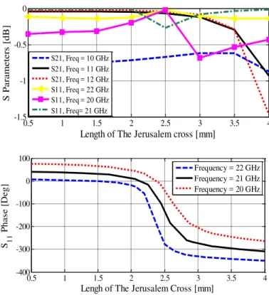
The S parameters obtained with explained method is compared with the S parameters from CST
and ADS in figure 3. The ADS S parameters are achieved by the technique mentioned in [12]. These
curves are drawn for the parameters mentioned above and ldk=2.5mm and θs=0 (normal incidence).
From these figures it is obvious that the curves achieved by different simulators match with each other
very well. To explore performance with variation of phasing element size, S11 and S21 amplitudes for
different values of ld are demonstrated in figure 4. Results show good transmission and suitable
reflection for various sizes of phasing elements at 10-12 GHz and at 20-23 GHz, respectively. As it is
clear from figure 4 the designed FSS- backed unit cell shows suitable performance in a wide
frequency range at both bands. The reflection phase and amplitude at K band and transmission
amplitude at X band are brought in figure 5 with use of CST parameter sweep. Phase variation of
about 360, reflection amplitude better than 0.3 dB at 21 GHz and appropriate transmission amplitude
(better than 0.7 dB) at 11 GHz are attained by this unit cell.
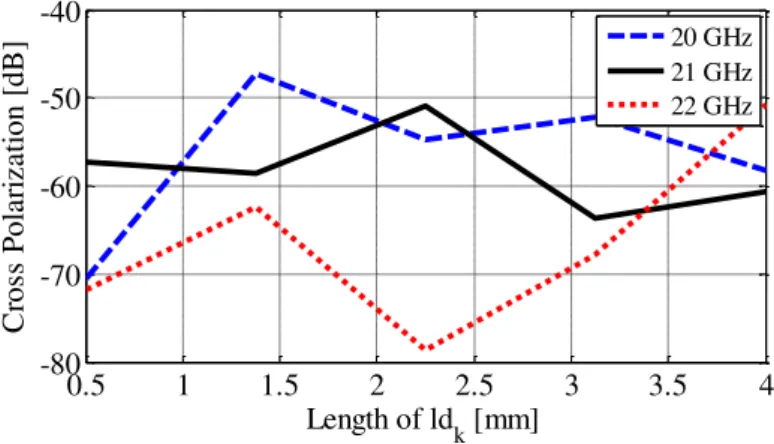
The effect of incident wave angle is an important issue which should be considered to have broad
band performance. The phase and amplitude of S11 are plotted in figure 6.a and b. As it is clear from
figures, this unit cell is less sensitive to the incident angle. Furthermore, the discussed unit cell has a
very low cross polarization. In figure 7 cross polarization versus length of ld is drawn for different
frequencies.
0 0.5 1 1.5 2 2.5 3
x 1010
-80 -60 -40 -20 0
Frequency [Hz]
S
P
ar
am
et
er
s
[dB
]
Matlab S21 ADS S21 CST S21 Matab s11 ADS S11 CST S11
Fig. 3. S21 and S11 amplitude versus frequency.
0 5 10 15 20 25 30
-60 -50 -40 -30 -20 -10 0
Frequency [GHz]
S
P
a
ra
m
e
te
rs
[
dB
]
S11, ld k= 4 mm
S11, 1d k= 2.5 mm
S11, 1d k= 1 mm
S21, 1d k= 1 mm
S21, 1dk = 2.5 mm
S21, 1d k= 4 mm
Fig. 4. S11 and S21 amplitude for different length of ldk.
X band
0.5 1 1.5 2 2.5 3 3.5 4 -1.5
-1 -0.5 0
Length of The Jerusalem cross [mm]
S P a ra m e te rs [ dB ]
S21, Freq = 10 GHz S21, Freq = 11 GHz S21, Freq = 12 GHz S11, Freq = 22 GHz S11, Freq = 20 GHz S11, Freq= 21 GHz
0.5 1 1.5 2 2.5 3 3.5 4
-400 -300 -200 -100 0 100
Lengh of The Jerusalem Cross [mm]
S 1 1 P ha se [ D e g]
Frequency = 22 GHz Frequency = 21 GHz Frequency = 20 GHz
Fig. 5. a) S21 amplitude at X band and S11 amplitude at K band b) phase of S11 at K band versus length of ldk.
0.5 1 1.5 2 2.5 3 3.5 4
-400 -300 -200 -100 0 100
Length of ld
k [mm]
P ha se of S 11 [D e g] Tetha=0, Phi=0 Tetha=20, Phi=0 Tetha =30, Phi=0 Tetha =0, Phi=45 Tetha =0, Phi=90
0.5 1 1.5 2 2.5 3 3.5 4
-1.4 -1.2 -1 -0.8 -0.6 -0.4 -0.2 0
Length of ld
k [mm]
S P ar am et er s [dB ]
S21, Freq=11 GHz, Phi=0, Theta=0 S21, Freq=11 GHz, Phi=30, Theta=20 S21, Freq=11 GHz, Phi=45, Theta=30 S11, Freq=21 GHz, Phi=45, Theta=30 S11, Freq=21 GHz, Phi=0, Theta=0 S11, Freq=21 GHz, Phi=45, Theta=20
0.5 1 1.5 2 2.5 3 3.5 4 -80
-70 -60 -50 -40
Length of ld
k [mm]
C
ros
s
P
ol
ar
iz
at
ion
[dB
] 20 GHz
21 GHz 22 GHz
Fig. 7. cross polarization versus length of ldk for different frequencies.
The Figures 8 and 9 present current surface distribution of the suggested element under
illumination of the y-polarized incident plane wave at 21 GHz and 11 GHz, respectively. These
figures are drawn for different phases of propagative wave at both 21 GHz and 11 GHz. As it is seen,
the current in the y direction is stimulated and current in the x direction is near zero at 21 GHz so this
structure has low cross polarization. The incident current flow at 11 GHz is near zero which means
the incident wave is mostly transmitted at this frequency as it is expected.
Fig. 8. Current distribution at 21 GHz for ldk = 3 mm. a) Phase of incident wave is 0. b) Phase of incident wave is 180.
Fig. 9. Current distribution at 11 GHz for ldk = 3 mm. a) Phase of incident wave is 0. b) Phase of incident wave is 90.
IV. K BAND ARRAY
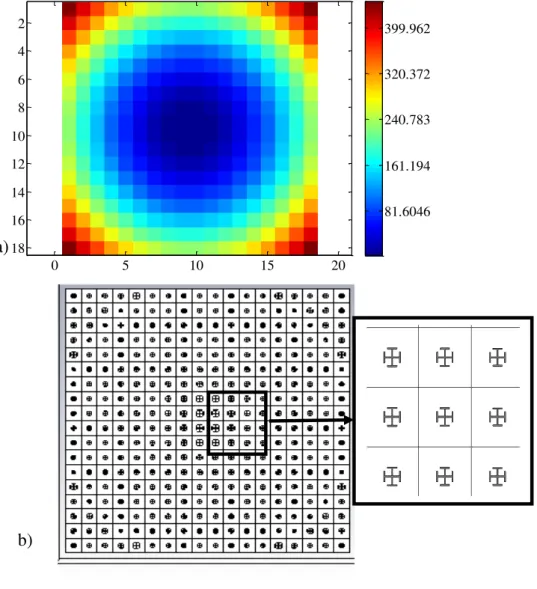
Using the unit cell element obtained in section II, 16.2 cm × 16.2 cm array is simulated. At first
step the required phase distribution on the array surface is computed with MATLAB and drawn in
figure 10-a. The simulated array using CST is shown in figure 10-b. The array is illuminated by a
linearly polarized horn antenna.
a)
a)
b)
The synthesized gain using MATLAB, the gain from CST and cross polarization is sketched in
figure 11. According to these results, the antenna has the maximum gain of 29 dB (50% efficiency)
and -40 dB cross polarization. The antenna gain versus frequency is plotted in figure 12 which proves
10% bandwidth for 1 dB gain variation. In section V these results are compared with previous works.
0 5 10 15 20
2
4
6
8
10
12
14
16
18
81.6046 161.194 240.783 320.372 399.962
Fig. 10. a) Phase distribution. b) The simulated array.
-100 -50 0 50 100
-40 -30 -20 -10 0
Azimuth [Deg]
N
or
m
a
li
z
e
d
P
a
tt
e
rn
[dB
] Synthesized Pattern
CST Co-pol Cst Cross-pol
Fig. 11. K band pattern.
a)
20 20.5 21 21.5 22 22.5 26
27 28 29
Frequency [GHz]
G
ai
n
[dB
]
Fig. 12. Gain versus frequency.
V. X BAND ARRAY
A conventional metal back unit cell is used at X band. Phasing element is the Jerusalem cross
dipole depicted in figure 13. The adjusted parameters for this unit cell are shown in figure 13 and they
are as: lu= 13 mm, ls=2 mm, w=1 mm. More than 700 degree phase variation is achieved with this
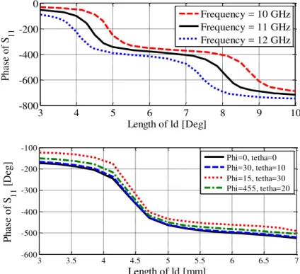
modified element. Phase variation versus length of ld are shown in figure 14 for normal incidence at
different frequencies and figure 14-b shows phase variation for different incident angles. The results
prove X band unit cell has little sensitivity to the incident angle.
Symmetric shape of the suggested unit cell leads to have low cross polarization. This
characteristic is investigated in figure 15. Also, Surface current is drawn for the unit cell at 11 GHz
under illumination of a y-polarized incident wave (figure15). As it is seen, surface current is induced
in y direction. The results of these figures prove little cross polarization at different frequencies.
Fig. 13. X band reflective element.
l
ul
sw
ld
ld/3
w/3
w
3 4 5 6 7 8 9 10 -800
-600 -400 -200 0
Length of ld [Deg]
P
ha
se
of
S 1
1
Frequency = 10 GHz Frequency = 11 GHz Frequency = 12 GHz
3 3.5 4 4.5 5 5.5 6 6.5 7
-600 -500 -400 -300 -200 -100
Length of ld [mm]
P
ha
se
of
S 1
1
[
D
eg]
Phi=0, tetha=0 Phi=30, tetha=10 Phi=15, tetha=30 Phi=455, tetha=20
Fig.14. S11 phase variation versus length of ld a) for different frequencies b) for different incidence angle.
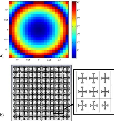
To study this modified unit cell performance, a 28.6 cm × 28.6 cm array is designed and 32mil
RO4003 is considered as substrate. Figure 17-a shows phase distribution on the surface of this array
and figure 17-b is the array simulated using CST.
3 4 5 6 7
-100 -80 -60 -40
Length of ld [mm]
C
ros
s
P
ol
ar
iz
at
ion
[dB
] 10 GHz
11 GHz 12 GHz
Fig. 15. Cross polarization versus length of ld.
Fig. 16. Current flow at 11 GHz. a) Phase of incident wave is 0. b) Phase of incident wave is 180.
-0.1 -0.05 0 0.05 0.1 -0.1
-0.05
0
0.05
0.1 50
100 150 200 250 300 350
Fig. 17. a) Phase distribution on the X band surface. b) The simulated array using CST.
To achieve dual band performance, K band array is placed on top of the X band. A 2 cm spacer
separates X and K RAs. The simulated co and cross polarization at 10.75 GHz are brought in figure
18. The efficiency of X band antenna is 60% and after placing K band it is reduced to 54%. A 0.5 dB
insertion loss is demonstrated from the figure. Figure 19 shows the simulated gain versus frequency
which verifies 1 dB gain bandwidth of 9% for X band in presence of K band.
-100 -50 0 50 100
-40 -30 -20 -10 0
Azimuth [Deg]
N
or
m
al
iz
ed
P
at
te
rn
[dB
] co pol with k band co pol without k band
cross pol without k band cross pol with k band
Fig. 18. Normalized pattern and cross polarization of X band array.
a)
10.25 10.5 10.75 11 11.25 11.5 25
26 27 28 29
Frequency [GHz]
G
ai
n
[dB
]
Fig.19. The simulated gain versus frequency.
The performance of our designed antenna is compared with previous dual band works in table 1.
Comparing pervious works with our proposed antenna, it is concluded this antenna has better
efficiency in both bands. Also, this works has better bandwidth in comparison with [1]. So it is
concluded the proposed antenna introduced in this communication has better efficiency and its 1 dB
bandwidth is acceptable. Also due to symmetric shape of the unit cell, it has a very low cross
polarization.
TABLE I. COMPARISON OF THIS WORK WITH PERVIOUS WORKS.
Reference [2] [9] [1] [6] This Work
Frequency (GHz) 8.5
18
10
13.58
8.4
32
10.2
22
11
21
Efficiency 40%
36%
51%
51.4%
52% (with Ka band)
60% (without Ka
band)
42%
47%
25%
54% (with K band)
60% (without K
band)
50%
1-dB BW
(%)
11%
12%
5.5%
2.9%
0.5%
1.5%
16%
9.1%
9%
10%
SLL(dB) <-16
<-15
<-22
<-20
<-16
<-20
<-15
<-20
-15
-18
Cross-Pol
(dB)
No Data -27
-27
-30
-20
-23
-25
-40
-40
VI. CONCLUSION
A new analytical method to design FSS-backed RAs is suggested in this communication. With the
use of this technique, a dual band antenna is designed and simulated. This suggested antenna operates
at X and K band with 54% and 50% efficiency, respectively. Also 1dB gain bandwidth of X band and
K band are 9% and 10%, respectively. Due to symmetric shape of the offered unit cell, the attained
cross polarization is low (about -40 dB). The results are compared with previous works which prove
good operation for designed antenna.
[1] M. R. Chaharmir, J. Shaker, and H. Legay, “Dual-band Ka/X reflectarray with broadband loop elements,” IET Microw. Antenna Propag.,vol. 4, lss. 2, pp. 225-231, 2010.
[2] Iman Derafshi, Nader Komjani, Ensieh Ghasemi-Mizuji and Mohammad Mohammadirad,” Dual-band X/Ku
Reflectarray Antenna Using a Novel FSS-Backed Unit-Cell with Quasi-Spiral Phase Delay Line” JMOE, Vol. 15, No.
3,pp 225-236 ,2016.
[3] C. Han, J. Huang, and K. Chang, “A high efficiency offset-fed X/Ka-dual-band reflectarray using thin membranes,”
IEEE Trans. Antenna Propag.,vol. 53, no. 9, pp. 2792-2798, Sep. 2005.
[4] M. R. Chaharmir, J. Shaker, N. Gagnon, and D. Lee, “Design of broad-band, single layer dual-band large reflectarray
using multi open loop el-ements,”IEEE Trans. Antennas Propag.,vol.58, no. 9, pp. 2875–2883,Sep. 2010.
[5] I. Derafshi, N. Komjani and M. Mohammadirad, “A Single Layer Broadband Reflectarray Antenna by Using Quasi
-spiral Phase Delay Line,” IEEE AWPL,vol. 14, pp. 84-87, 2014.
[6] R. Shamsaee Malfajani and Zahra Atlasbaf, “Design and Implementation of a Dual-Band Single Layer Reflectarray in
X and K Bands IEEE Trans. Antenna Propag., VOL. 62, pp4425-4430, 2014.
[7] M. Rafaei-Booket, Z. Atlasbaf, and M. Shahabad, “Broadband Reflectarray Antenna on a Periodically Perforated
Substrate” IEEE Trans. Antenna Propag., vol.64, pp 3711 - 3717, 2016.
[8] Rafael Florencio, José A. Encinar, Rafael R. Boix, Vicente Losada and Giovanni Toso, “Reflectarray Antennas for
Dual Polarization and Broadband Telecom Satellite Applications”, IEEE Trans. Antenna Propag., VOL. 63, NO. 4, pp
1234 – 1246, 2015
[9] Fei Xue, Hongjian Wang and Min Yi1, “Design of X/Ku Dual-Band Dual-Linear Polarization Reflectarray Using
Double Parallel Dipole Elements” Progress In Electromagnetics Research C, Vol. 66, pp11–20, 2016.
[10]J. Huang and J. A. Encinar, Reflectarray Antennas. New York: IEEE Press, Wiley-Interscience, 2008.
[11]L. Li, Q. Yuan, K. Sawaya, T. Maruyama and T. Furuno, “Frequency Selective Reflectarray Using Crossed-Dipole
Elements With Square Loops for Wireless Communication Applications” IEEE Trans. Antenna Propag., vol.59, pp
89-99, 2011.
[12]Mahmoud Fallah, Alireza Ghayekhloo and Ali Abdolali,” Design of Frequency Selective Band Stop Shield Using
Analytical Method”, Journal of Microwaves, Optoelectronics and Electromagnetic Applications, Vol. 14, No.
2,pp217-228, December 2015
[13]C. R. Simovski, P. De Maagt, and I. V. Melchakova, “High-impedance surfaces having stable resonance with respect to
polarization and incidence angle“,IEEE Trans. Antenna Propag., vol.53, pp 908-914, 2005.
[14]M. R. Chaharmir and J. Shaker, “Design of a Multi-Layer X/Ka-Band Frequency Selective Surface- Backed