*e-mail: [email protected]
Trabalho apresentado no XV CBECIMAT, Natal - RN, Novembro de 2002.
Sb Doping Effects and Oxygen Adsorption in SnO
2Thin Films Deposited
via
Sol-Gel
Viviany Geraldoa, Luis Vicente de Andrade Scalvib*, Evandro Augusto de Moraisa,
Celso Valentim Santillic, Sandra Helena Pulcinellic
aInstituto de Física de São Carlos, USP
C.P. 369, 13560-970 São Carlos - SP, Brazil
bDepartamento de Fisica - FC, UNESP
C.P. 473, 17033-360 Bauru - SP, Brazil
cInstituto de Química de Araraquara, UNESP
C.P. 355, 14801-970 Araraquara - SP, Brazil
Received: January 29, 2003; Revised: August 31, 2003
Transparent electrically conducting antimony-doped SnO2 thin films have been prepared by sol-gel dip-coating process from colloidal aqueous suspension. The effect of doping content on the structural, optical and electrical properties is analyzed. Results from infrared optical transmission and reflection have shown that the higher the Sb concentration the lower the transmission intensity and the higher the reflection signal. Absorption intensity increases as well. Results of X-ray reflectometry and electron microscopy have shown that the density of films fired at 400 °C after each dip is higher than that of multi-dipped films prepared with a single annealing. Both the electrical characteristics in the dark and the increase in conductivity as function of illumination through differ-ent filters, at 190 K, evidence that the transport properties of these films are dominated by the pres-ence of defects, including the trapping at grain boundary due to excess of oxygen.
Keywords:tin dioxide, nanostructures, sol-gel, optical properties
1. Introduction
Tin dioxide is an n-type, wide bandgap semiconductor (about 3.5 eV) and in the form of thin films, it is a transpar-ent conducting material, characterized by high optical
trans-mission (80-90%)1. Optical, electrical and structural
prop-erties make tin dioxide very attractive for many kind of ap-plications in opto-electronic devices2, gas sensors3-5 and solar
collectors6,7. Moreover, doping tin dioxide with electronic
donors as F- or Sb5+ yields a high conductivity without
sig-nificant changes in its optical transmittance8. Conducting
SnO2:Sb films exhibit increasing absorption coefficient in
the infrared, where absorption spectra can be reasonably
well described by Drude’s free electron gas theory9,10.
Trans-mission coefficient decreases with increasing thickness and
doping levels2, while reflection in the infrared region
in-creases with increasing Sb concentration10,11.
SnO2 films properties are strongly influenced by
prepa-ration technique. The sol-gel process presents many advan-tages compared to other techniques, such as excellent ho-mogeneity, thickness control and possibility of coating large and complex surfaces, using both inorganic and organic pre-cursors, whereas alkoxids precursors are expensive and ex-tremely sensitive to moisture, producing inhomogeneous layers when prepared under room atmosphere. The colloi-dal suspensions prepared via inorganic sol-gel route devel-oped in our laboratory have been a preferred way to making
SnO2 films by dip coating, because these disadvantages are
fea-ture is generally attributed to a combination of effects asso-ciated to the nanoscopic characteristic of sol gel materials, like reduced crystallite size, high porosity in combination with doping segregation and gas adsorption of gaseous spe-cies at the surface of the crystallites.
In this work, we present an analysis of the effect of Sb
doping to polycrystalline SnO2 thin films deposited via
sol-gel route with several concentrations of Sb (1.5, 2, 3 and 4%) on their electrical and optical properties. In order to improve the film density and examine the effect of nanostructural feature on their optical and electrical prop-erties, two distinct post-deposition annealing procedures were used, whose difference is basically a firing step at 400 °C between each dip.
2. Experimental
Colloidal suspensions of Sb-doped SnO2 nanoparticles have
been prepared from Sn4+ aqueous solution (0.25 mol/l),
ob-tained by dissolution of SnCl45H2O and SbF3 (Merck).
Hy-drolysis was promoted by addition of ammonium
hydrox-ide (NH4OH) under magnetic stirring until pH reaches 11.
The precipitate obtained by this way, was submitted to di-alysis in order to eliminate as much as possible chloride, fluoride and ammonium ions. This procedure leads to stable
SnO2:Sb colloidal suspensions for several doping
concen-trations. These suspensions, were used for film deposition on silicate glass substrates by dip-coating technique, with a withdrawing rate of 10 cm/min. Multi-dipped films were deposited basically following two procedures, concerning firing between dips. They are described below:
Procedure I (PI) - After each dip, which takes place at room temperature, films are kept in air for 20 min and then dried in a oven at 50 °C by 30 min. When the desired number of layers is obtained, films are annealed at 500 °C for 1 h under air or vacuum.
Procedure II (PII) - the only difference to procedure I is that between each dip, the deposited film is fired at 400 °C for 10 min. In other words PII allows a significant increase on intermediate annealing temperature, which is carried out after each layer deposition.
Infrared transmittance and reflection have been meas-ured by a Nicolet spectrophotometer in the range
1.8-12 µm. X-ray reflectometry measurements have been
done in a reflection chamber coupled to a conventional
pow-der diffractometer Siemens D5000, using CuKα
monochro-matic radiation. The accuracy in the incident and detection angles was 0.001° and the width of both entrance and re-ceiving slits were 0.01 mm to minimize the angular diver-gence. Simulation of experimental reflectivity curves has been done on the basis of the formalism developed by
Nèvot-Croce12 by means of the Refsimul software, developed by
Siemens, which supplies the following structural parameters:
i) apparent density, deduced from the critical angle; ii) thick-ness of the film deduced from the periodic oscillations and iii) interface roughness deduced from the amplitude of the periodic oscillations. To verify the thickness of multi-dipped films, scanning electron microscopy is carried out on sam-ples with 50 dips, grown by both procedures. This is done with a Microscope Stereoscan 440-LEO.
To perform electrical measurements, In electrodes have been evaporated on the samples through a shadow mask in a Edwards evaporator system. Electrodes are annealed to 150 °C by 20 min in air. Low temperature electrical meas-urements were done in an Air Product Cryostat which con-trols temperature in the range of 25 to 300 K within 0.1 K of precision.
The average crystallite size has been determined from
X-ray diffraction peaks, using Scherrer method13, where the
particle size decreases with half width increase. The broad-ening of half width is evaluated considering the
contribu-tion of grain size and due to instrument broadening13.
3. Results and Discussion
3.1. Sb doping Influence on the infrared spectra
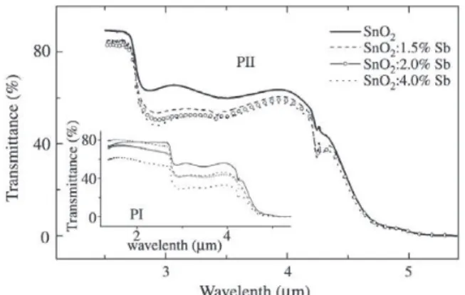
Figure 1 shows optical transmittance in the infrared of films prepared by both procedures. Main Fig. 1 shows the
transmittance in the 2.4 to 5.4 µm range for samples
ob-tained by procedure PII whereas inset of Fig. 1 shows
in-frared transmittance in the range 1.8 to 5.4 µm for PI films.
In both cases the transmittance decreases as Sb concentra-tion increases.
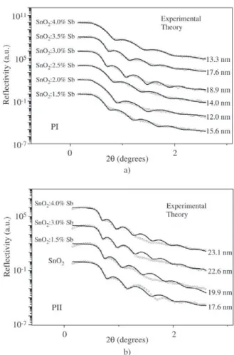
Figure 2 shows infrared reflection for PII films. Reflec-tion increases with Sb concentraReflec-tion, in good agreement with transmittance data. Regions of lower transmittance are
incident with reflection maximum, meaning that the re-flected fraction of the incident beam is probably more sig-nificant than absorption fraction in the infrared range. Small
bands observed about 3.4 and 4.2 µm may be related to
hydroxyl groups14 that were not completely eliminated by
annealing at 500 °C. Usually hydroxyl groups begin to be eliminated at 250 °C but they are not completely desorbed at 500 °C15.
Evaluation of bandgap transition from optical absorp-tion data in the ultraviolet to visible range yields an average value of 3.6 eV for indirect transition, in good agreement
with expected energy (3.5-4.0 eV)16.
In near infrared region the classical Drude theory ap-plies, whenever the carrier concentration is high enough to allow plasma resonance phenomena. Then, reflection in in-frared region increases with increasing Sb concentration.
The plasma resonance frequency ωp is given by11:
ωp2 = (4 π N e2).(ε
mεo m*)
-1 (1)
N is the free electron concentration, εm and εo represent dielectric constants of medium and free space respectively
and m* is the effective mass of conduction band. The
com-plex dielectric constant ε(ω) can be given by17:
ε(ω) = 1 - ωp2/ ω2 = 1 - λ2 / λ p
2 (2)
where λp is the plasma resonance wavelength. If ε is real
and negative (λ> λp), solutions of the wave equation decay exponentially so that no radiation can propagate through the film. Then a high reflection is expected. If e is positive
(λ< λp), solutions become oscillatory and radiation can
propagate. Estimation of free electron concentration from electrical resistivity data have yielded up to 5 × 1018 cm-3,
which would correspond to about 15 µm for λp. It means
that the whole range shown in Fig. 1 and 2 are below the
plasma resonance wavelength, and then, radiation should not be reflected. In order to describe the observed optical reflection in the infrared region of these films, concentra-tion as high as 1020 cm-3 is needed10,11. The decreasing trans-mittance with increasing Sb concentration observed on films grown by both methods suggests that films may have in-deed a high free carrier concentration in the neutral bulk region, but there is also a very high electron scattering at boundary layer. Sol-gel films used in our measurements have
small grain size (3-10 nm) 18 and their resistivity is rather
large. Then there is a large amount of crystallites concomi-tant with potential barrier at grain boundary which is
re-lated to large grain boundary depletion layer19. It leads to a
strong electron scattering at grain boundary. Besides the presence of pores must be taken into account since it de-creases the electron free path. Therefore the electron mo-bility of these sol-gel films is unusually low and it is re-sponsible for the high resistivity observed in these films (see Fig. 5).
Figure 2. Near infrared reflection spectra for SnO2:Sb thin films deposited by PII.
3.2. Influence of firing on SnO
2 :Sb film deposition Figure 3 shows the experimental X-ray reflectivity and fitted curves for samples obtained by PI and PII. Figure 3a shows results for single dipped films obtained by PI. The critical angle (θC), corresponding to total reflection, is in-variant within experimental error, indicating that samples
have the same density (≅ 3.6 ± 0.2 g/cm3). This low value
indicates about 47% of pores when compared to SnO2
sin-gle crystal. The periodicity of oscillation observed for
θ > θC indicates that films are continuous, presenting an
uniform thickness. The film thickness, deduced from the period of oscillation, is in the range 12.0 nm to 18.9 nm, when Sb concentration is varied, even though no propor-tionality between thickness and Sb concentration is
ob-served. Particularly for SnO2:1.5%Sb films (composition
used for MEV experiments - see next paragraph) the layer thickness is 15.6 nm. Figure 3b corresponds to X-ray reflectometry results and fitted curves for films obtained by PII. Films used in this case have 3 dips since 1 dip films obtained by this procedure turned out to be too thin and did not yield good simulation results. The density obtained from simulation parameters is about
4.7 ± 0.1 g/cm3, which indicates a porosity of about 33%.
These films also present continuous increase in thickness of 17.6 nm to 23.0 nm as the Sb content increases from 0.0 to 4.0%. Since these experimental curves correspond
to films prepared with 3 dips, each layer of SnO2:1.5%Sb
film has average thickness of 6.6 nm.
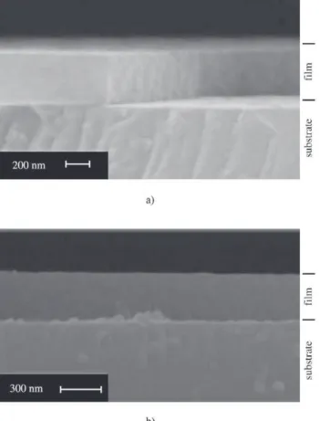
Figure 4 shows scanning electron microscopy (SEM)
results for SnO2:1.5%Sb films prepared by both procedures,
with 50 dips. As it can be seen, the film prepared by PI (Fig. 4a) is about 400 nm thick, whereas film prepared by PII is about 300 nm thick. A qualitative analysis indicates that SEM results agree with X-ray reflectometry results, which means that temperature of 400 °C for firing between dips (PII) decreases film thickness, since in both kinds of measurements PI yields thicker films than PII. The average thickness per dip calculated from these values are 8 nm and 6 nm for PI and PII, respectively. Then, a further compari-son between results of SEM and X-ray reflectometry, yields that the agreement is much better for PII than PI, which suggests that using PII the structural feature of single dipped layer is essentially preserved after multiple dip. On the other hand, the thickness of each successive layer prepared by PI decreases as the number of dip application increases. This feature may be related to a higher porosity obtained from PI (47%), which suggests the existence of much more empty space, and a softer film which could either be more easily fulfilled by precursor solution or partially peeled during the upper layer application. As a consequence, it results in a non-homogeneous structure and a worse optical transmit-tance.
3.3. Electron trapping
Resistivity as function of temperature measured in the dark, for the range of 25 to 300 K is shown in Fig. 5 for a few films grown by procedure PII. The increase in the
con-ductivity at 190 K for SnO2:4%Sb film when submitted to
tungsten light of 160 W, driven towards the region between contacts through a filter, is given in the inset of Fig. 5, whose cut-off wavelength is the x-axis. It is clearly seen that Sb doping increases n-type conductivity even though the resis-tivity is still rather high. It is interesting to mention that when
SnO2 films are annealed under vacuum its resistivity
de-creases. A similar film to that of Fig. 5 with 4%Sb, when annealed at 500 °C, under vacuum, presents resistivity of
9.3 × 10⁻³ ohm.m at room temperature. However this is not
a permanent effect. Exposure to atmospheric air recovers the high resistivity. An Arrhenius plot of curves of Fig. 5 (not shown) yields activation energy of 144, 42 and 38 meV for the deepest level (ionized at higher temperature range)
of undoped SnO2, SnO2:3.5%Sb and SnO2:4.0%Sb
low donor of antimony doping and the deeper one agrees
with oxygen vacancy20. It is also interesting to mention that
doubly ionized vacancies have also been taken as
responsi-ble for electron trapping in SnO2 as published elsewhere21.
In this case the values obtained could be related to first ion-ized state of oxygen vacancy (30 meV) and the deeper
at-tributed to the second ionized level of oxygen vacancy20.
Since our undoped sample does not present a shallower level about 30 meV, our conclusion is that 144 meV indeed cor-responds to oxygen vacancy level and 38 to 42 meV are Sb donor ionization levels (slightly shifted with Sb concentra-tion). The high resistivity observed in these films suggests the existence of another trapping level, which is not tem-perature dependent. The main effect of electron trapping in this defect is the increase of depletion layer around grain boundary, which decreases the mobility, and thus the con-ductivity. Sb donors that contribute to the conductivity are located in the very center of crystallites and are also re-sponsible for infrared optical reflection as already dis-cussed. The inset of Fig. 5 shows ionization of different levels inside the bandgap, so that when the bandgap
transi-tion is overcame (lc < 280 nm) the conductivity is greatly
increased (more than 1000% over the dark value). It is in-teresting to mention that this increased conductivity is “fro-zen” when illumination is removed. Only when the sample is heated, conductivity returns to room temperature value. This kind of measurement assures that there are states in-side the bandgap which can be photoexcited. However it is difficult to associate them with the ionization energies ob-tained from Arrhenius plot, since deep level defects may show large Stokes shift, which is usually related to
vacancy-like defects22. The high intensity of the excitation lamp also
Figure 5. Resistivity as function of temperature for SnO2 thin films prepared by PII, with 30 dips and 3 different Sb compositions. Inset - relative increase in the conductivity as function of illumina-tion using filters with several different cut-off wavelengths, meas-ured at 190 K.
assures that either the concentration of these defects is small (the conductivity increases only a little) or they have photoemission energy very close to bandgap transition.
4. Conclusion
Infrared optical transmission of SnO2 thin films,
depos-ited by dip-coating via sol-gel, decreases with increasing Sb doping. This behavior can be explained based on Drude’s free electron gas theory. In our films, reflection in the near infrared is due to a large amount of free electrons in the crystallite bulk region. In this case, the high resistivity is related to strong grain boundary scattering.
The firing process between each dip during deposition of
SnO2 thin films turned out to be responsible for a more
com-pact arrangement of layers leading to more dense and thin-ner films concomitant with less pores. Besides this firing at 400 °C between dips promotes better agreement between X-ray reflectometry and SEM results, which means that as the number of dips increase, films submitted to intermediate annealing keep their thickness proportional to the number of deposited layers, whereas films with no firing between dips are subject to a shrinking as the deposition goes on.
Energy levels obtained from Arrhenius plot indicate the presence of vacancy-like defects. The low excitation with infrared illumination, and the increase of conductivity only close to bandgap transition suggest intra-bandgap trapping levels with large Stokes shift.
Although methods used here for sample preparation yields films with improved morphology and optical trans-mission, conductivity is still low and probably can be in-creased by elimination of excess of oxygen from grain boundary layer and other defects.
Acknowledgments
The authors wish to thank Prof. Ligia O. Ruggiero and Prof. Margarida J. Saeki for helping us with the technical setup. We also thank Brazilian financial sources for finan-cial help: CAPES, CNPq, FAPESP and PRONEX.
References
1. Dien, E.; Laurent, J.M.; Smith, A. J. European Ceramic
Soc., v. 19, p.787, 1999.
2. Terrier, C.; Chatelon , J.P.; Roger, J. AThin Solid Films v. 295, p. 95, 1997.
3. Guglielmi, M.; Menegazzo, E.; Paolizzi, M.; Gasparro,
G.; Ganz, D.; Putz, J.; Aegerter, M.A. J. Sol-Gel Sci.
Technol. v. 13, p. 679, 1998.
4. Nakata, S.; Ojima, N. Sensors and Actuators B, v. 56,
p. 79, 1999.
5. Heilig, A; Barsan, N; Weimar, U; Gopel, W. Sensors and
6. Sanon, G; Rup, R; Mansingh, E.A. Phys. Rev. B, vol. 44, p. 5672, 1991.
7. Geoffroy, C.; G. Campet, G.; Merril, F.; Portier, J.;
Salardenne, J.; Couturier, G. Active and Passive Elec.
Comp., v. 14, p. 111, 1991.
8. zum Felde, U.; Haase, M.; Weller, H. J. Phys. Chem. B,
v. 104, p. 9388, 2000.
9. Rockenberger, J.; zum Felde, U.; Tischer, M.; Troger, L.;
Haase, M. ; Weller, H. J. Chem Phys., v. 112, p. 4296,
2000.
10. Nutz, T.; Haase, M. J. Phys. Chem. B, v. 104, p. 8430,
2000.
11. Santhi, E.; Dutta, V.; Banerjee, A.; Chopra, K.L. J. Appl.
Phys. v. 51, p.6243, 1980.
12. Nèvot, L.; Croce, P.; Rev. Phys. Appl., v. 15, p. 761,
1980.
13. Cullity, B.D. Elements of X-ray Diffraction,
Addson-Wesley Pub. Comp., Massachussetts, 1978.
14. Lin, Y.J.; Wu, C.S. Surface Coatings Technology, v.88,
p. 239, 1996.
15. Yamazoe, N.; Fuchigami, J.; Kishikawa, M.; Seiyama, T. Surf. Sci., v. 86, p. 335, 1979.
16. Kololuoma, T.; Rantala, J.T. Electron. Lett., v. 36,
p. 172, 2000.
17. Ashcroft, N.W.; Mermin , N.D. Solid State Physics, CBS
Publishing, Philadelphia, p. 18, 1976.
18. Scalvi, L.V.A.; Messias, F.R.; Souza, A.E.; Siu Li, M.;
Santilli, C.V.; Pulcinelli, S. H. J. Sol-Gel Sci. Technol.,
v. 13, p. 793, 1998.
19. Messias, F.R.; Vega, B.A.V.; Scalvi, L.V.A.; Siu Li, M.;
Santilli, C.V.; Pulcinelli, S.H. J. Non-Crystalline Solids,
v. 247, p. 171, 1999.
20. Zarzebski, Z.M.; Marton, J.P. J. Eletrochem. Soc,. v.
123, p. 299C, 1976.
21. Samson, S.; Fonstad, C.G. J. Appl. Phys., v. 44, p. 4618,
1973.
22. Lang, D.V.; Logan, R.A.; Jaros, M. Phys. Rev. B, v. 19,