Growth of YBCO Superonduting thin Films on
CaF
2
Buered Silion
S.S. Bhagwat,A.R. Bhangale,J.M. Patil,and V.S.Shirodkar
SolidStateEletronisLaboratory, Departmentof Physis,
TheInstitute ofSiene,15 Madam,CamaRoad, Mumbai -400 032,India
Reeived25Otober,1999. Revisedversionreeivedon15May,2000
CaF
2
lmsweregrown on<100 >silion usingthe neutral luster beamdeposition tehnique.
These lms werehighly rystallineand -axis oriented. Superonduting YBCOthin lmswere
grownontheCaF
2
bueredsilionusingthelaserablationtehnique. TheselmsshowedT(onset)
at 90K and T(zero) at 86K. X-ray diration analysis showed that the YBCO lms were also
orientedalongthe-axis.
I Introdution
Sine the disovery of superondutivity in YBCO
muheorthasbeenput todeposit itasthin lmson
silionsubstrates,owingtoitspotentialappliationsin
miroeletronis. However, during the annealing
pro-ess athigh temperaturessilionfromthesubstrateis
found to diuse into the YBCO lms, severely
aet-ingthesuperondutivity, transitiontemperature(T
)
and urrent density ( J
) [1-3℄. Toprevent this
dele-terious diusion of Si into thesuperonduting lm a
suitablebuerlayerisfoundneessarytointerpose
be-tweenSiandYBCO.Caliumuoridehasshowngood
thermalexpansionorrespondingtosilionandYBCO
lms. The lattie mismath between CaF
2
and Si is
0.6% at room temperature, while for [011℄/[001℄
rela-tionshipbetweenYBCOandCaF
2
,amismathof0.8%
alongYBCOa-axisand1.1%alongtheb-axisexists[4℄.
Hene in the presentstudy CaF
2
bueredSi hasbeen
used forfabriating YBCO thin lms. Theaimof the
presentstudy is to investigate theminimum thikness
of CaF
2
required to stopthe migration of Si into the
superonduting lm. The riterionused for this
pur-poseistheT
valueandthesharpnessofthetranstion
whihisdisplayedbysmalltransition widthT
. The
hoieofYBCO washowever,madeonthebasisthat,
itis oneofthemoststablehigh T
superondutor.
II Experimental
Caliumuoridepowder(99.99%purity,Aldrih
Chem-ials, USA) was used to develop the buer layer on
Si using the neutral luster beam deposition
teh-nique. Thepowderwashargedinaspeiallydesigned
peratureThedetailsoftheruibledesignandother
as-pets ofneutrallusterbeamdepositiontehniqueare
desribedelsewhere[5℄. Thesilion<100>substrates
were leaned using the standard leaning proedure.
Priorto thedeposition,the silionwafersweredipped
indilute HNO3forafewseonds andthenthoroughly
rinsedin distilled water. These waferswere dried and
loadedin theworkhamberfordeposition. TheCaF
2
deposition wasarriedin theworkhamberevauated
to 10 6
mbarpressure using anEdwards Co. (U.K.)
turbo-moleularpumpbakedbyarotarypump.
Dur-ingthedeposition thethiknessoftheCaF
2
lmswas
monitored using a Maxtek lm deposition ontroller
model FDC 440and wasross- heked using Dektak
thiknessprolometer.
A KrF (248 nm) eximer pulsed laser (Lambda
Physik model 301i) having a pulse width of 25ns and
1 to 10 Hz repetition rate with maximum energy of
1200mJwasusedfortheablationofYBCOonbuered
silionfrom itssintered pellet. Sinetheintensity
pro-leof30mm20mmlaserbeamhasagaussion
distri-butionalongtheshortaxis,only5mmofentralregion
of thebeam was allowed to passthrough anaperture
with 5mm height and 10mm width. The beam was
foussed onto the target to get 3mm 0.8mm spot
size with the help of a quartz lens of 200mm foal
length. Prior to the YBCO thin lm growth the
de-position hamber was evauated to the base pressure
of510 6
mbarusingaTurbomoleularpump (V
ar-ian 2000) baked by a mehanial rotary pump. AR
grade oxygen was introdued in the hamber, during
thedeposition,theowofwhihwasontrolledusinga
rotameter. Agatevalvewasusedtothrottletheturbo
tainedat760 Æ
CThethiknessoftheYBCOlmswas
measuredusingtheDektakthiknessprolometer. The
superonduting lms were haraterized using
om-puterizedresistivitymeasurementset-up(omprisingof
Keithley urrent souremodel220, Keithley
multime-termodel199,Lakeshoretemperatureontrollermodel
DRC 91C),JoelX-ray diratometermodel 8030and
Joelsanningeletronmirosopemodel840. The
an-gular resolutionof theX-ray diratometeris loseto
0.05 Æ
.
III Results and disussion
Fig. 1 shows the X-ray diration pattern of 165nm
thikCaF
2
buerlayeron<100>silionannealedfor
1houratoptimumtemperatureof650 Æ
C[5℄. Itisseen
that only <001 >peaksappear whih indiates that
the buer layers has C-axis orientation. In addition,
averysmall magnitudeof FWHM,0.082,
orrespond-ing to < 004 > peak suggests the lm to be highly
rystalline in nature. Fig. 2 shows the x-ray
dira-tionpattern of theYBCO lms deposited onbuered
silion. These YBCO lms had athiknessof the
or-der of 450nm. A large number of < 001 >
orienta-tions along with a few other random orientations are
observed. Forexampletheintensity peakat 21
orre-spondsto(003)orientation,whilethepeaks at30and
39 are of (004) and (005) orientation respetively. A
fewunknown peaks whih aremarkedwith asteriskin
thegurearealsoseentobepresent. Theharateristi
peakofCaF
2
appearsat70 Æ
whihorrespondsto(004)
orientation. Fig. 3 shows the resistane Versus
tem-peratureplotsofYBCOlmsgrownonCaF
2
layersof
dierentthiknesses. AlltheYBCOlms,depositedon
CaF
2
ofdierentthiknesses,were450nmthik. Curves
markeda,b andorrespondto theCaF
2
layerswith
thikness of 120nm, 150nm, and 165nm respetively.
All thelmsweredeposited underidentialdeposition
onditionsand were given sameannealing treatments.
It is seen from the gure that the urve 'a' does not
showthepreseneofsuperondutivityinYBCOlms
grownon120nmCaF
2
buer. Thenature oftheurve
'b' shows that the lm initially behaves like a
semi-ondutorand then transformsinto superondutivity
with T
(onset) at86K andT
(zero) at 70K.The
na-tureoftheR-TurveinFig. 2showsthat theYBCO
deposited on 165nm thik CaF
2
retains its
superon-dutivitywithT
(onset)90Kand T
(zero)86K.These
valuesareingoodagreementwiththereportedvalues.
[6℄. TheR(300,to R(,00)is about2.8whih is
india-tiveofgoodmetalliity. Alsotheabsolute valueofthe
resistivityofourYBCOlmisoftheorderof2-3
m-mat 300Kand isintheaeptablerange[7℄. Thusit
anbeseenthattheminimumthiknessofCaF
2 buer
to realizesuperonduting YBCO on silionsubstrate
isabout165nm.
Figure1. X-rayDirationpatternof165 nmthikCaF
2
buerlayeron<100>Silion.
Figure 2. XRD pattern of the YBCO lm deposited on
bueredsilion.
Figure3. ResistaneVsTemperatureplotsofYBCOlms
grownonCaF2 layersofdierentthikness.
It is known that [8℄ CaF
2
tends to loose uorine
duringthehightemperatureannealingtoformCaSiO4.
This oxidation ofsilion andformation of alium
sil-iate beginsat theSi/CaF
2
interfae and proeed
to-wardsCaF
2
surfaewhereYBCO is deposited. Hene
dependingontheannealingtemperatureapartofCaF
2
layerneartosilionwillbeonvertedtoCaSiO
4 owing
tothemigrationofSi. WehaveseenthatYBCOgrown
150nm CaF
2
it displayssuperondutivitywith broad
transition width. Thismaybeattributedtomigration
of Si impurity into the YBCO lm resulting into
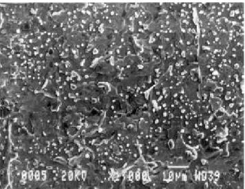
in-omplete buereet. Indeedasrevealed bysanning
eletronmirographshowninFig.4asizeablenumberof
miroraksandvoids,togetherwithoutgrowthsatthe
juntions of the oalesentgrains are apparent. Thus
the transition temperatureof theYBCO lm redued
withtheinreaseintransitionwidth.
TheR-Turveshownin Fig. 2() revealsthat the
lmismetalliinnatureandtransformsinto
superon-dutivity withT
(onset)at 90Kand T
(zero) at 86K.
It was found that YBCO lms grown on CaF
2 layer
havingthiknessmorethan165nmshowedmoreorless
idential R-TurvesandT
valueasthatobtainedfor
lmsgrownon165nmCaF
2 layer.
Figure4. SEMphotographofYBCOlmgrownon150nm
CaF2 Buer.
IV Conlusion
Itis possibleto growhighlyrystalline -axisoriented
buers on silion using Neutral Cluster beam (NCB)
deposition tehnique. The YBCO lms deposited on
buered silion showed T
(Zero) at 86K, whih is in
good agreement with those reported for YBCO on
CaF
2
. It is also seen that the minimum thikness of
CaF
2
buerlayertoeetivelystopthemigrationofSi
intothelmsis about165nm.
Referenes
[1℄ H. Nakajima, S. Yamasuhi, K. Iwasaki, H. Morita,
H.Fujimori andF.Fujino, Appl.Phys.Lett.53,1437
(1988).
[2℄ G. Koren, E. Polturak, B. Fisher, D. Cohen and G.
Kimel,Appl.Phys.Lett.53,2320 (1988).
[3℄ T.Venkatesan, E.W.Chase,X.D.Wu,A.Inam,C.C.
Chang, F.D. Shokoohi, Appl. Phys. Lett. 53, 243,
(1988).
[4℄ A.N. Tiwari, S. Blunier, H. Zogg, Ph.Lerh,
F.Marenat and P. Martinoli. J. Appl.Phys.71, (10)
15May1992.
[5℄ S.S.Bhagwat,A.R.Bhangale,J.M.Patil,V.S.
Shirod-kar R.Pinto, P.R.Apte, S.P. Pai, Braz. J.Phys,29,
338(1999).
[6℄ KeizoHarada, Hidenori N. Hideo I,Shuji, Y., JJAP,
30(5),5thMay1991.
[7℄ DhananjayKumar, M. Sharon, R.Pinto, P.R.Apte,
S.P. Pai, S.C. Purandare, L. C. Gupta and R.
Vija-yaraghavan,Appl.Phys.Lett.62(26),3522 (1993).
[8℄ A.Lubig,Ch. Buhal,J.Frohlingsdorf, W.ZanderB.