Brazilian Microwave and Optoelectronics Society-SBMO received 14 Feb 2013; for review 21 Feb 2013; accepted 16 Apr 2013
On the Design of Nano-arm Fractal Antenna
for UWB Wireless Applications
Raj Kumar and 1Sheetal Gaikwad
Microwave and Millimeter wave Lab., DIAT (DU), Girinagar, Pune-411025,India 1
M. Tech. (Microwave Engg)
Pune Institute of Computer Tech., Pune, India
Email:dr.rajkumarkumar@yahoo.com
Abstract – This paper presents the design of a nano-arm fractal antenna suitable for ultra wide band applications. The CPW-feed and fractal concept have been used to achieve the ultra wide bandwidth. The shape of the fractal geometry, the number of iterations and the number of nano-arms are the deciding factors for achieving wider impedance bandwidth. The experimental result of the fractal antenna exhibits ultra wideband characteristics in the frequency range of 2.55 GHz to 11.84 GHz corresponding to an impedance bandwidth of 131.77%. The measured radiation patterns of the proposed antenna are nearly omni-directional in the H–plane and bidirectional in the E-plane. The antenna can be useful for modern wireless communication, medical imaging and ground penetrating radar.
Index Terms – Planar Monopole antenna, Multiband antenna, Fractal
Geometry, CPW - Feed and UWB System
I. INTRODUCTION
The recent progress in UWB wireless communication applications has remarkably increased the
demand for wideband antennas with smaller dimensions than conventionally possible [1]. The antenna
size with respect to the wavelength is the parameter that will have an influence on the radiation
characteristics, gain and efficiency. Conventional microstrip antenna has limitations of narrow
bandwidth, low gain and size of /2 [1-2]. There are several techniques reported in the open literature
to improve the bandwidth of the microstrip patch antenna such as insertion of air gap, stacking,
ground coupling etc. The coupling effect is possible by changing the feed type and selecting proper
values for its parameters. CPW feed offers better resonant characteristics and higher impedance
bandwidth. [3-4].
The fractal geometry along with the CPW feed can be used for achieving ultra wide bandwidth [4].
The fractal geometry is supported by its two properties i.e. self similarity and space filling [5]. The
self-similarity property is useful for multiband or ultra wideband (UWB) feature while space filling
property is useful for antenna miniaturization. Using these properties, several UWB monopole
antennas have been reported in the literature [6-11]. This paper presents an UWB antenna with
andwidth beyond the required FCC band. Several modifications in the antenna structure like adding
achieve the desired impedance bandwidth. A detailed parametric analysis has been presented and
discussed. The simulated results of this antenna have been validated with experimental results.
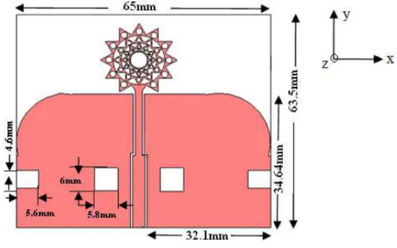
The fractal antenna structure taken for investigation is shown in Figure.1. This fractal antenna is
designed on a substrate of dielectric constant r = 4.3, thickness 1.53 mm and with dimensions
63.5 mm x 65 mm. The fractal antenna is constructed from a solid circular disc of radius 12.5 mm as
shown in Fig. 1.
Fig. 1. Four iterative Concentric Nano-arm fractal antenna and its side view
This fractal antenna is constructed by using a set of scaled versions of the same shape which is
similar to the concept of Sierpinski Gasket. In the first iteration, the perimeter of the circular patch is
divided into twelve equal arcs, on the inner side of each arc; an isosceles triangle is drawn with an
angle of 40 degrees from the perpendicular bisector of each node (edge of each arc). The resultant
shape appears to be a chain of twelve inward looking triangles. This portion is etched off from the
base. As a second step in the first iteration, eleven circular slots of 1 mm diameter have been drawn
having their centres at a distance of 3.75 mm on the inner side of each node (except for the node near
the feed) on the line connecting the node and the centre. These circular slots are then etched off the
base. The resultant geometry from here onwards is referred to as the generator. This constitutes the
first iteration.
The 2nd iteration is a reduced copy of the design of the first iteration, repeated in an inner circle of
8.125 mm radius (which is 0.65 times of 12.5mm). Likewise the third and the fourth iterations are
repetitions of their previous ones at a reduced ratio of 0.62, within the concentric circles. The infinite
iterative structure which is ideally perceivable is not practically possible because of fabrication
constraints. So for the present investigation, a fourth iterative Fractal Antenna is finalized and
extensively studied with respect to its characteristics.
The CPW feed and its parameters such as the gap between the feed and the ground and the width of
the feed are the critical factors which decide proper impedance matching. For the initial stage, they
Brazilian Microwave and Optoelectronics Society-SBMO received 14 Feb 2013; for review 21 Feb 2013; accepted 16 Apr 2013 with better radiation characteristics. Every dimension of the proposed antenna has been optimized to
give the most appropriate results.
II. CURRENT DISTRIBUTION
The surface current density distribution is simulated at 2.3 GHz for the proposed fractal antenna
corresponding to the first, second, third and fourth iterations and is illustrated in Fig. 2. Maximum
current distribution is observed near the gap between the feed and the ground, on the edges of the
radiating patch, on the ground near to the patch, and along the x-axis of the ground plane. That is why
the size of the patch, the width and the length of the ground plane, the gap between the ground and the
patch, the gap between the ground and the feed, all are crucial parameters for achieving the wide
impedance bandwidth and need to be optimized.
Fig. 2. Surface current density at 2.3 GHz for four iterations
III. SIMULATED RESULTS AND DISCUSSIONS
The proposed fractal antenna has been designed on the substrate of permittivity r = 4.3 and
thickness 1.53 mm. The substrate size of the antenna has been taken as 63.5 mm x 65 mm. The
antenna was designed and fabricated with optimized dimension. A parametric study of the antenna
was carried out using HFSS software based on the Finite Element Method.
Initially, the fractal monopole antenna is simulated with the simple circular patch of radius 12. 5mm
with CPW feed. The ground plane length and width are taken to be 34.64 mm and 31.1 mm. But with
this circular patch and rectangular ground plane, the required UWB impedance bandwidth is not
achieved. The twelve nano - arm fractal antenna as shown in Fig. 2 is simulated with respect to the
various parameters for achieving the UWB characteristics. The parametric study with respect to
various parameters is discussed below.
A. Effect in the Number of Iterations
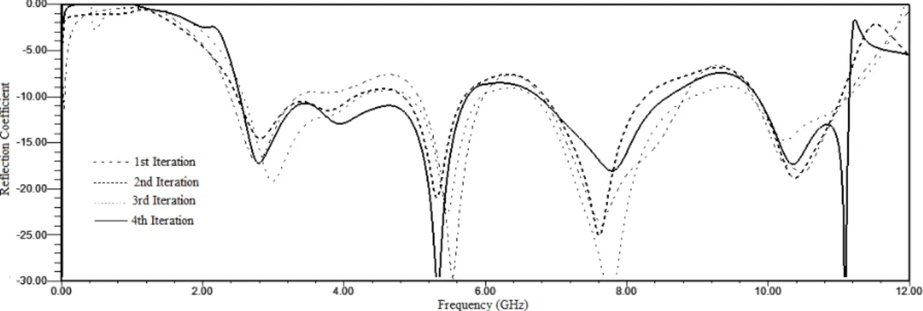
The parametric study with respect to the number of iterations has been performed. The iterative
behaviour of the fractal antenna is carried out and shown in Fig. 3. The circular microstrip patch
geometry, the resonant frequency is shifted to the lower frequency side at 2.2 GHz. This is due to the
increase in the resonant length due to the application of fractal geometry. The application of fractal
leads to the reduction in the size of the patch. There is a distinct shift in the fundamental resonant
frequency dip as the number of iterations goes on increasing.
Fig. 3. Effect on the return loss characteristics due to increase in iterations
As the number of iterations increases, the first resonant frequency dip on the reflection coefficient
curve shifts to the lower frequency side as illustrated in Fig. 3. It is also observed that the reflection
coefficient improves as iteration increases through out the band. As seen in Fig. 3, the reflection
coefficient is poor for the first iteration but improves substantially at the fourth iteration through out
the operating band. This is one of the importance characteristic of fractal geometry that impedance
matching improves with proper number of iterations. It means no extra circuitry is required for the
impedance matching of a fractal antenna. This behaviour of the antenna is observed till the fourth
iteration. So, a fouth iterative twelve nano-arm fractal antenna is considered for further investigation.
This antenna is said to exhibit -10 dB reflection coefficient bandwidth in the frequency range of 2.6
GHz to 11.8 GHz.
B. Effect of Ground Plane Length (GL)
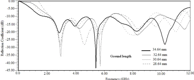
The length of the ground plane plays a vital role in determining the UWB characteristics. The effect
on the reflection coefficient characteristics of the variation in the ground length is shown in Fig. 4.
The ground plane length is varied in steps of 2 mm from 28.64 mm to 34.64 mm. As the length of the
ground plane increases, the reflection coefficient curve is shifted to the lower frequency side. This is
clearly observable near the second, third and fourth dips of the reflection coefficient curve shown in
Fig. 4. It is observed that better performance is achieved at 34.64 mm ground length throughout the
band.
Brazilian Microwave and Optoelectronics Society-SBMO received 14 Feb 2013; for review 21 Feb 2013; accepted 16 Apr 2013
Fig. 4. Effect of variation in length of the ground plane
C. Effect of Ground Plane Width (Gw)
Here, the width of the ground plane of the proposed fractal monopole antenna is varied and its effect
on the antenna bandwidth is observed. The proposed antenna has been simulated for various ground
plane widths (GW) from 27.2 mm to 31.2 mm. The simulated results with respect to various ground
widths (GW) are shown in Fig. 5. It is observed that as the ground width increases the first resonant
frequency shifts to the lower frequency side. The optimum ground width obtained by fixing all other
optimized parameters is 31.2 mm for optimum impedance matching throughout the band. For values
smaller and larger than the optimized ground width, the optimum impedance bandwidth is disturbed.
It means that there is one value of ground width for optimum impedance matching.
D. Effect of Gap between Patch and Ground (GP-G)
The gap between the patch and the ground is also a critical factor in determining the impedance
bandwidth of the antenna. Hence, a parametric analysis with respect to the gap between the patch and
the ground is done with respect to the fourth iterative fractal antenna. The behaviour is observed by
varying the gap (GP-G) in steps of 0.1 mm. The gap between the patch and the ground is varied to 0.4
mm, 0.5 mm, 0.6 mm, and 0.7 mm and their corresponding reflection coefficient characteristics are
shown in Fig. 6.
There is no one to one correspondence between the change in the reflection coefficient and the gap
between the patch and the ground. As the ground plane is closer to the radiating patch, most of the
fields will be radiated and less fringing fields reside in the substrate.
Fig. 6. Variation of gap between patch and the ground
No noticeable change in the bandwidth is observed here. An increase in the gap between the patch
and the ground results in decreasing the reflections which in turn leads to an improvement in the
return loss. It also results in the maximum coupling of signal between them. The optimum reflection
coefficient in the frequency range of 2.2 GHz to 11.0 GHz is obtained for the gap of 0.6 mm
according to Fig. 6.
E. Effect of the Gap between the Feed and the Ground
This twelve nano-arm fractal antenna is fed with CPW feed and it is well known that for better
impedance matching, the gap between the feed and the ground, and the width of the feed are the
deciding parameters. Here the width of the feed is kept constant at 3.2 mm. The gap between the feed
and the ground is selected so as to provide best matching for the 50 ohm line. The separation between
the feed and the ground was optimized over various values to yield wider bandwidth. The optimum
gap between the ground and the feed is obtained as 0.5 mm. At this gap, the impedance is around 50
Brazilian Microwave and Optoelectronics Society-SBMO received 14 Feb 2013; for review 21 Feb 2013; accepted 16 Apr 2013
Fig. 7. Effect of the separation between feed and ground
The reflection coefficient characteristics for different values of the gap between the feed and the
ground are shown in Fig. 7. For this particular configuration, the gap between the feed and the ground
is kept as 0.5 mm. After parametric optimization, the gap between the patch and the ground is kept as
0.6 mm and the length of the ground as 34.64 mm. There is only minor variation in the impedance
bandwidth with respect to the width of the ground. Hence the width of the ground plane is kept as
32.1 mm. The width and the height of the substrate is taken as 63.5 mm and 65 mm. The simulated
VSWR plot in the frequency range of interest is shown in Fig. 8. It is observed that the VSWR is less
than 2 in the range from 2.6 GHz to 11.8 GHz.
Fig. 8. VSWR of proposed twelve nano arm fractal antenna
F. Modified Ground Plane
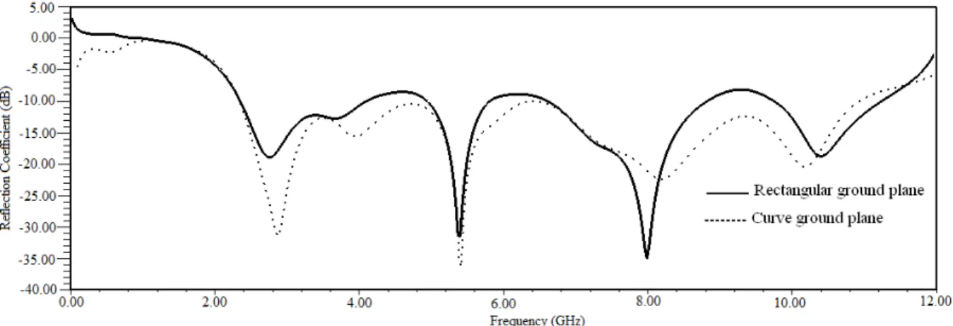
It was difficult to get the reflection coefficient of the antenna below -10 dB. To improve the
slots in the ground plane. The simulation results with the simple rectangular ground plane and with
the modified ground plane are shown in Fig. 9.
Fig. 9. Simulated reflection coefficient with and without modified ground
IV. EXPERIMENTAL, SIMULATED RESULTS AND DISCUSSION
The proposed fractal antenna with CPW - feed is shown in Fig. 1. The antenna was fabricated with
optimized dimensions and tested. The experimental results were acquired using Vector Network
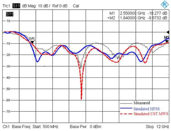
Analyzer R & S ZVA40. The experimental result exhibits the impedance bandwidth from 2.55 GHz to
11.84 GHz corresponds to 131.77 %. The experimental result shows the resonance dips at frequencies
2.875 GHz, 5.45 GHz, 8.05 GHz and 10.35 GHz as shown in Fig. 10. The simulated resonance dips
are evident as current maxima (red colour) on the feed line and the ground plane as shown in Fig. 11.
These resonance dips merge with each other to give the overall impedance bandwidth from 2.55 GHz
to 11.84 GHz. This antenna was simulated using HFSS and CST Microwave studio software. The
measured results are compared with simulated results. The measured result are in close agreement
with the simulated results obtained from HFSS and CST MWS software as shown in Fig. 10. There is
a slight devation between the two simulated results. This is because both the software are based on
different Numerical techniques. There is also slight deviation between experimental and simulated
results. This deviation may be because of fabrication tolerances, uncertainty in substrate thickness and
Brazilian Microwave and Optoelectronics Society-SBMO received 14 Feb 2013; for review 21 Feb 2013; accepted 16 Apr 2013
Fig. 10. Mesured and Simulated Reflection Coefficient of proposed twelve nano arm fractal antenna
Fig. 11. Simulated current of proposed fractal antenna for multiple resonance dips as current maxima (Red colour )
The radiation patterns in the two principal planes viz, the E-plane and the H-plane were measured
in the inhouse anechoic chamber. The radiation patterns were measured at selective frequencies. The
H – plane radiation patterns were measured at 3.0 GHz, 4.05 GHz, 4.95 GHz, 6.0 GHz, 7.05 GHz,
8.25 GHz, 10.35 GHz and 11.32 GHz. And are shown in Fig. 12. The simulated radiation patterns in
the H- plane from HFSS and CST MWS software are calculated as shown in Fig. 13. The nature of
the H – plane radiation patterns is nearly omnidirectional. The measured and simulated radiation
patterns are in close agreement. Similary, E – plane radiation patterns were measured at 3.85 GHz, 4.8
GHz, 6.075 GHz, 7.05 GHz, 8.1 GHz, 9.45 GHz, 10.95 GHz and 11.55 GHz. The E – plane radiation
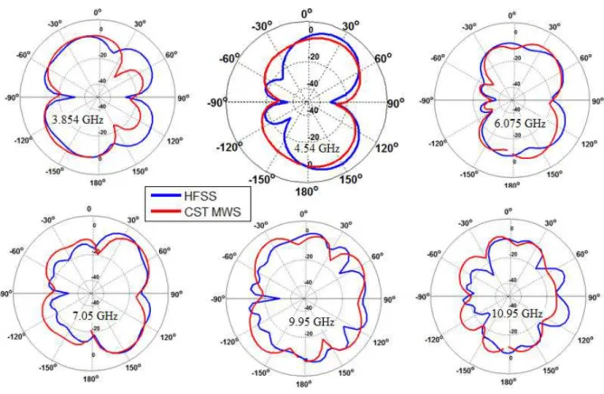
patterns are shown in Fig. 14. The simulated radiation patterns in E- plane from HFSS and CST MWS
in the E –plane. The radiation patterns in both the planes slightly deteriorate as the frequency goes on
increasing. This may be due to the higher magnitude of higher modes at higher frequencies and the
fractal geometry of the antenna. At lower frequencies omni directional nature of radiation patterns in
H - plane and bidirectional nature of radiation pattern in E - plane are evident.
Brazilian Microwave and Optoelectronics Society-SBMO received 14 Feb 2013; for review 21 Feb 2013; accepted 16 Apr 2013
Fig. 14. Measured radiation patterns in E – plane at 3.85, 4.8, 6.075, 7.05, 8.1, 9.45,10.95 and 11.55 GHz
Fig. 15. Simulated radiation patterns in E – plane at 3.854, 4.54, 6.075, 7.05, 9.45 and 10.95 GHz
The peak gain and radiation efficiency of the antenna have been simulated using HFSS and CST
microwave studio software. The simulated peak gain of the antenna is shown in Fig. 16. The
simulated peak gain calulated from HFSS is very close to that calculated from CST microwave studio.
Brazilian Microwave and Optoelectronics Society-SBMO received 14 Feb 2013; for review 21 Feb 2013; accepted 16 Apr 2013 numerical techniques. The peak gain increases as the frequency increases. It is because at higher
frequencies the wavelength becomes shorter in comparison to the radiation patch size. The peak gain
beyond frequency 8 GHz is almost around 5 dBi. This is because, beyond this frequency cross
polarization loss as well substrate loss increases. The simulated radiation efficiency is also in very
good agreement from both the software (HFSS and CST Microwave studio) as shown in Fig. 17. The
radiation efficiency decreases as the frequency increases. It reduces to 65 % at 12 GHz from 90 % at 3
GHz . This is because lossy dielectric FR4 substrate of dielectric constant r = 4.4 and thickness h =1.6
mm was used.
Fig. 16. Simulated peak gain of proposed antenna
V. CONCLUSIONS
A fractal antenna suitable for UWB applications is designed and experimentally validated. The
parametric study of the antenna with respect to various design parameters has been performed to
obtain ultra wide bandwidth. The proposed fractal antenna exhibits wide band characteristics in the
frequency range from 2.55 GHz to 11.84 GHz corresponding to the impedance bandwidth of 4.64:1.
The modification in the ground plane improves the -10 dB reflection coefficient bandwidth
throughout the band. The radiation pattern of the antenna has been found to be nearly
omni-directional in the H-plane and biomni-directional in the E-plane. This property of the antenna makes it a
suitable candidate for modern UWB applications. The antenna is compact, light weight, low cost,
simple to fabricate and easy to integrate with MIC/MMIC devices. The antenna may be useful for
applications like modern wireless communication, precision positioning systems, ground penetrating
radar, vehicular radar and medical imaging.
VI. ACKNOWLEDGMENTS
We would like to thank the Vice Chancellor of DIAT (Deemed University), Girinagar, Pune for all
the support and encouragement. We would also like to thank the staff of Department of Electronics
Engg., Ph.D. and M. Tech. students of the Microwave and Millimeter wave Antenna Lab for their
support.
REFERENCES
[1] D. L. Werner, “On fractal electrodynamics :Recent Advances in Electromagnetic Theory”, H.N. Kritikos and D. L. Jaggard (eds.),183-224, Springer-Verlag, New York, 1990.
[2] D. H. Werner and S. Ganguly, “An overview of Fractal antenna engineering research”, IEEE, Antenna and Propagation Magazine, Vol. 45, No. 1, 38-57,2003.
[3] J. Liang, C. Chiau, X. Chen and J. Yu, “Study of a circular disc monopole antennas for ultra wideband applications,” 2004 International Symposium on Antennas and Propagation, 17-21 August, 2004.
[4] J. Liang,et.al, “CPW-fed circular disc monopole antenna for UWB application”, IEEE International Workshop on
Antenna and Technology: Small Antennas and Novel Meta materials, Marina Mandarin, Singapore, March 7–9, 2005, pp. 505–508.
[5] Min Ding et. al. “Design of a CPW-fed Ultra Wideband Crown Circular Fractal Antenna” MOTL, Jan. 2007, pp. 173-176.
[6] Raj Kumar, Dhananjay Magar and K. K. Sawant,”On the design of inscribed triangle circular fractal antenna for UWB applications”, Int. Journal of Electronics and Communication (AEU), Jan. 2012, pp. 68-75, Germany.
[7] Raj Kumar and Prem Narayan Choubey, ”Modified L – shape CPW-feed of UWB fractal antenna”, IJMOT, Vol.6, No.4, pp. 197-202, 2011,USA
[8] Ding, R. Jin, J. Geng, and Q. Wu, “Design of a CPW-fed ultrawidebandfractal antenna”, Microwave Opt Technol.
Lett. 49 (2007),173-176.
[9] Leonardo Lizzi, and Andrea Massa,”Dual-Band Printed Fractal Monopole Antenna for LTE Applications,” IEEE
Antennas and Wireless Propagation Letters, Vol. 10, pp.760 – 763, 2011.
[10] Homayoon Oraizi and Shahram Hedayati,” Wideband Monopole Fractal Antenna with Hilbert Fractal Slot Patterned Ground Plane,” Proceedings of the 41st European Microwave Conference, pp. 242-245, Manchester, UK, 10-13 October 2011.
