Abstract—This work reports the development of a simple, low-profile and ultra-wideband printed antenna. The proposed antenna is based on a truncated ground plane and an impedance matching structure formed by a round junction and two chamfers; these modifications significantly increase the antenna frequency bandwidth compared to conventional microstrip antennas and ultra-wideband printed monopoles published in literature. An antenna prototype was fabricated using an Arlon DiClad 880 substrate with an electrical permittivity of 2.2. A bandwidth of 176% was attained at a central frequency of 14.9 GHz (ranging from 1.79 to 28.02 GHz). Numerical simulations and experimental
results of the antenna’s radiation pattern are also reported and exhibit good agreement. To the best of our knowledge, this is the widest bandwidth from a printed antenna that has been published in the literature.
Index Terms—Broadband antennas; printed antennas; truncated ground plane; ultra-wideband antennas.
I. INTRODUCTION
The electromagnetic spectrum consists of an infinite range of frequencies, but only a portion of
them is used for wireless communications systems due to equipment limitations and other factors,
such as attenuation. Given the large number of technologies and wireless communications standards
covering numerous applications, the spectrum is currently congested, especially for frequencies up to
6.0 GHz. The current regime of fixed frequency allocation adopted by regulators has been criticized
due to the inefficiency of the allocation and spectrum scarcity. The licensed spectrum is often unused
or partially used at any given time or place. Therefore, it becomes necessary to apply technologies to
explore its use in a smart, efficient and dynamic manner [1]. In 1999, Joseph Mitola proposed the
concept of cognitive radio (CR) [2]. This technology proposes the use of an intelligent radio that is
able to automatically detect available channels in the frequency spectrum and change transmission
parameters, thus permitting a greater volume of data to be exchanged simultaneously.
Beyond the cognitive radio, there are other telecommunications technologies, such as the
ultra-wideband (UWB) system, that require broadband antennas [5]. The UWB is formed from two pairs of
radios, one working as a transmitter and the other as receiver. The radio sends and receives pulses
with a short duration of approximately 1 ns [6]. The pulses are transmitted in the wide spectral range
of 3.1 to 10.6 GHz at a low power level. The power spectral density is reduced by spreading the signal
over this wide frequency band, which minimizes interference with other systems [7]. Ideally, an
A low-profile and ultra-wideband printed
antenna with a 176% bandwidth
R. A. Santos and Arismar Cerqueira S. Jr.
antenna applicable to this technology would be compact, flat and low cost [8].
Several approaches have been proposed to design wideband antennas [8-11], such as double-ridged
horn antennas, Vivaldi antennas, conical antennas, log-periodic antennas and TEM horn antennas.
There are also some articles on ultra-wideband printed monopoles antennas [12-18] with fractional
bandwidth, corresponding to a reflection coefficient of less than -10 dB, of up to 116.67% [18], as
summarized in Tab. I. A. Mehrdadian et al. proposed a large-fit antenna based on a combination of a
TEM horn antenna and magnetic dipoles that provides a fractional bandwidth of 197% [9]. The main
drawback of this antenna is its size, which is extremely large compared to printed antennas. There is
an increasing need to develop antennas with small dimensions that can be used in nearly any location.
Tab. I. Example of printed ultra-wideband antennas.
Antenna Fractional
Bandwidth (%)
Frequency range (GHz)
Printed Circular Disc Monopole [6] 116.26 2.69 to 10.16
CPW-fed two-layered monopole antenna [7] 117.30 3.76 to 14.42
Ultra Wide-band Printed Monopole [8] 104.70 3.3 to 10.55
Low-Cost PCB Antenna [9] 103.45 3.5 to 11
A Printed Monopole Antenna With Two Steps and a Circular Slot [10] 116.67 3 to 11.4
This paper proposes a simple, low-profile and ultra-wideband antenna aimed to address the
requirements of cognitive radio, UWB and measurement device applications. The antenna is based on
a truncated ground plane and an impedance matching structure that is formed by a round junction and
two chamfers. This technique significantly increases the frequency bandwidth to overcome the main
drawbacks of conventional microstrip antennas.
II. ULTRA-WIDEBAND PRINTED ANTENNA
This section is focused on the development of the proposed ultra-wideband printed antenna and its
main electromagnetic properties. Initially, the printed antenna theory is presented, with the purpose of
giving a basic background on the subject. Posterior, we present the ultra-wideband design based on a
modified microstrip antenna with some impedance matching structures. Finally, the antenna
frequency response and radiation pattern characteristics are reported.
A. Printed Antenna Theory
Microstrip antennas, which were first devised by G. Deschamps in 1953 [13], provide many
advantages, such as easy and inexpensive manufacturing, compatibility with large-scale production
and easy adaptation for aerodynamic structures, such as aircraft, satellites and missiles. However, the
from 1% to 13% of the resonance frequency, depending on the manner in which the antenna is fed
[10,19-20]. The physical phenomenon behind this characteristic is their high merit factor (Q factor)
[20], quantified by:
1 máx w
máx VSWR B
Q VSWR
(1)
where VSWRmáx is the maximum voltage standing wave ratio, which is associated to the antenna
impedance matching. Therefore, it becomes to reduce the antenna Q factor for designing wideband
printed antennas. A Q factor reduction implies in reducing the stored power in the antenna, which
becomes capable of transmitting a higher level of RF power. In other words, the parcel of the radiated
power from the quality factor (Qrad) is reduced. Qrad is inversely proportional to effective Epson (εef):
0
1
4 ef
rad
f K
Q
h G
(2)
The resonance frequency of a conventional patch antenna is determined by its length L and the
substrate permittivity [10].
8
0
3 10
2
2
efL L
f
(3)The calculation can be improved by adding a “fringing length extension” ΔL, which comes from the
fringing fields along its radiating edges, to each patch edge, which results in an “effective length”. The antenna’s bandwidth is directly proportional to the substrate thickness h. However, if h exceeds
approximately 0.05 λ0, the probe inductance becomes large enough for matching to be difficult. Additionally, the antenna’s bandwidth is inversely proportional to rea and directly proportional to its
width W, in which rea is the average dielectric constant of the substrate and air [10].
8
0
3 10
2
reaW f
(4)Proper changes in the antenna structure and its ground plane size can significantly enhance the
microstrip antenna bandwidth. For example, M. Kundu et al. recently developed a broadband
microstrip-fed UWB printed monopole antenna based on four slots with the same arc radius at four
different corners and found a significant bandwidth enhancement (122%) [21]. Complimentarily,
Zeeshan Ahmed et al. proposed a CPW-fed planar monopole antenna that covers the UWB range, i.e.,
3.10 to 10.6 GHz, and efficiently rejects the WLAN bands from 5.15 to 5.35 GHz and 5.725 to 5.825
GHz [22].
B. Ultra-wideband Antenna Design
Our proposed ultra-wideband antenna consists of series of modifications to a conventional
ground plane (shown in dark gray color) of a conventional microstrip antenna (Fig. 1a) was truncated
to decrease its Q factor by reducing the dielectric constant [23] (Fig. 1b). The truncated ground plane
further increases the antenna bandwidth by improving the impedance matching between the
microstrip antenna and its feeding line [24]. It is responsible for creating a capacitive load that
counteracts the natural inductance of the microstrip antenna, making the antenna input impedance
(Zin) nearly purely resistive [25]. Additionally, a round junction was applied to the printed antenna
structure (Fig. 1c), which produces a smooth change in the impedance between the transmission line
and antenna patch, reduces the reflection coefficient and increases the antenna bandwidth. The final
step relies on chamfering the final two corners of the antenna-radiating element. The novel
ultra-wideband antenna structure that is based on a truncated ground plane, a round junction and two
chamfers and its primary design parameters are reported in Fig. 1d. Particularly, the chamfers provide
an improvement in the impedance matching at 27 and 29 GHz, as a result of a proper current
distribution in the resonator edges.
An Arlon DiClad 880A substrate was considered for the antenna design and used to fabricate a
prototype. The primary electromagnetic properties of this substrate are as follows: dielectric constant
r = 2.2; thickness t = 1.524 mm; and loss tangent tan( ) = 9x10 -4
. All antenna dimensions, including
those of the truncated ground plane, were numerically evaluated and optimized using the HFSSTM
(High Frequency Structural Simulator) software from ANSYS to obtain a low-profile and
ultra-wideband antenna. The final dimensions were as follows: a = 10 mm; b = 4.25 mm; f = 0.76 mm; L =
36.9 mm, which corresponds to one half of the guided-wavelength (λg/2) at 2.7 GHz; S = 60 mm; T =
60 mm; and W = 29 mm.
The resonant input resistance of a conventional patch antenna typically varies from 100 to 200 Ω
and is nearly independent of the substrate thickness h and proportional to r. The effective dielectric constant ef must be considered due to the air dielectric boundary. These considerations are indeed
valid for the proposed antenna, although diffraction that originates from the ground plane truncation
must also be considered. We numerically evaluated the real and imaginary parts of the input
impedance at each stage of the proposed antenna development. The antenna impedance matching was
progressively enhanced throughout the antenna development stages. Particularly, the final
modification on the radiating element, which included two chamfers, improves the antenna impedance
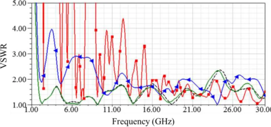
matching over frequencies from 15 to 18 GHz, which is illustrated in the voltage standing wave ratio
(VSWR) results in Fig. 2. The proposed antenna exhibits multiple resonances, wherein the impedance
reactive part assumes a zero value throughout its entire operating range, i.e., from 1.8 to 23.2 GHz.
Over this ultra-wide frequency range, the real part of the antenna’s impedance varies from 33 to 88 Ω,
whereas its imaginary part ranges from -26 to 22 Ω (see Fig. 3). These characteristics result in a
VSWR of less than 2.0, corresponding to a reflection coefficient of less than -10 dB and resulting in a
(a) Conventional microstrip antenna (CMA)
(b) Antenna with a truncated ground
plane (ATGP) Resonator
(c) Antenna with a truncated ground plane and a junction
(ATGPJ)
W T
S L
b
a f
(d) The proposed antenna (PA) and its primary design parameters
Ground plane
Fig. 1. The proposed low-profile and ultra-wideband antenna.
Fig. 2. VSWR simulation: red curves with rectangles (CPA); blue curve with triangles (ATGP); dashed black curve (ATGPJ); continuous green curve (PA).
C. Ultra-wideband Antenna Radiation Pattern
The conventional patch antenna approximately acts as a resonant cavity, i.e. short-circuit walls on
the top and bottom and open-circuit walls on its sides. In a cavity, only certain modes are allowed to
exist at different resonant frequencies. If the antenna is excited at a resonant frequency, a strong field
is formed inside the cavity with a strong current on the patch bottom surface. This effect produces
significant radiation and consequently increases the radiation efficiency, which corresponds to the
ratio of the power radiated into space to the total input power. The radiating patch length is typically
λg/2, which enables it to radiate. In our case, the first antenna resonance is centered at 2.7 GHz that corresponds to λg/2 for this frequency. Therefore, the conventional patch antenna is essentially a
broadside radiator, which has a relatively large beam width and low gain characteristics. Its electrical
field-plane pattern is typically broader than the magnetic field-plane pattern.
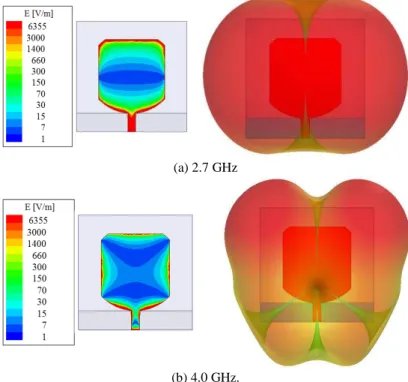
The proposed antenna radiation pattern is a result of the interplay between the longitudinal and
transversal modes with the truncated ground plane, which causes edge diffraction. It tends to degrade
the pattern by introducing rippling in the forward direction and back-radiation for high frequencies
because their corresponding wavelengths are much smaller than the ground plane dimensions.
Therefore, the electromagnetic waves for this frequency range are reflected (Fig. 4b). However, over
its lowest frequency range, i.e., from 1.79 to 3.50 GHz, the pattern consists of two separate radiating
slots that are separated by half of a wavelength (Fig. 4a). The guided wavelength is considerably
higher than the ground plane; thus, the radiation generated in the slits does not interfere with the
ground plane. As a result, an omnidirectional radiation pattern is formed.
(a) 2.7 GHz
(b) 4.0 GHz.
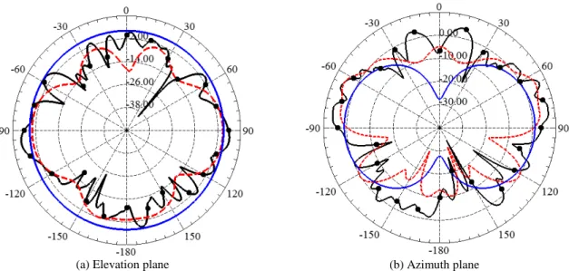
Fig. 5 illustrates radiation pattern for 2 GHz (blue continuous curve), 14 GHz (dashed red curve)
and 28 GHz (black curve with circles). Fig. 5a presents parallel plane (elevation) radiation pattern,
whereas Fig. 5b exhibits perpendicular plane (azimuth) radiation pattern. Meanwhile, diagram curve
from 2-GHz frequency carrier shows omnidirectional radiation pattern in azimuth and maximum gain
of 2.2 dBi. However, 14 and 28-GHz frequency operations demonstrate radiation pattern disturbed
because of increasing of propagation modes, in which their maximum gain are, respectively, 6.8 and
8.53 dBi.
(a) Elevation plane (b) Azimuth plane
Fig. 5. Radiation pattern simulation: blue continuous curve (2.0 GHz); dashed red curve (14 GHz); black curve with circles (28 GHz)
III. EXPERIMENTAL RESULTS
An antenna prototype was constructed using a substrate of Arlon DiClad 880A. Fig. 6 presents top
and bottom views of the antenna prototype, which was characterized using a vector network analyzer,
the MS4640B model from Anritsu. This model is capable of operating from 70 kHz to 70 GHz.
Initially, the antenna reflection coefficient (S11) was was performed using a K connector for printed
circuit boards, which operates up to 40 GHz. Thus, a good agreement between the simulations and
experiments was obtained, even for higher frequencies. The small discrepancy obtained for this case
is probably due to two reasons: the manufacturing process, in which the milling unintentionally
decreased the thickness of the substrate in some parts of the antenna, and variations in the substrate
permittivity at higher frequencies. The experimental results indicate a bandwidth from 1.79 to 28.02
(a) Front view. (b) Back view.
Fig. 6. Antenna prototype.
The next step was the radiation pattern characterization, in the semi-anechoic chamber from Inatel,
by using the following pieces of equipment: Keysight N5173B EXG, which is analogic signal
generation, Keysight N5952A FieldFox microwave analyzer; a log-periodic antenna, which operates
from 400 MHz to 6.0 GHz; a horn antenna that operates from 17 GHz to 28 GHz. Due to our
laboratory facilities, we measured the radiation pattern only at 3.0, 4.0, 5.8 and 17.0 GHz, as reported
in Fig. 8.
The antenna gain assumes lower values over its lowest bandwidth because it behaves as an
omnidirectional radiator for these frequencies. As soon as the frequency is increased, the
concentration of the radiation lobes is also increased, which means that its gain assumes higher values
(Fig. 9). The maximum absolute gain varies from 1.7 to 8.0 dBi over frequencies ranging from 1.79 to
28 GHz. Fig. 9 also presents three red crosses that represent measurements of the antenna gain at 3.0,
4.0, 5.8 and 17.0 GHz. An excellent agreement between the HFSS simulations and experimental
results is observed.
-10 -8 -6 -4 -2
0 0 10 20 30 40 50 60 70 80 90 100 110 120 130 140 150 160 170 180 190 200 210 220 230 240 250 260 270 280 290 300 310320 330340350
(a) Elevation plane at 3.0 GHz
-25 -20 -15 -10 -5
0 0 10 20 30 40 50 60 70 80 90 100 110 120 130 140 150 160 170 180 190 200 210 220 230 240 250 260 270 280 290 300 310 320330 340350
(b) Elevation plane at 4.0 GHz
-20 -15 -10 -5
0 0 10 20 30 40 50 60 70 80 90 100 110 120 130 140 150 160 170 180 190 200 210 220 230 240 250 260 270 280 290 300 310 320330 340350
(c) Elevation plane at 5.8 GHz
-25 -20 -15 -10 -5
0 0 10 20 30 40 50 60 70 80 90 100 110 120 130 140 150 160 170 180 190 200 210 220 230 240 250 260 270 280 290 300 310 320330 340350
(d) Azimuth plane at 3.0 GHz
-25 -20 -15 -10 -5
0 0 10 20 30 40 50 60 70 80 90 100 110 120 130 140 150 160 170 180 190 200 210 220 230 240 250 260 270 280 290 300 310 320330 340350
(e) Azimuth plane at 4.0 GHz
-30 -24 -18 -12 -6
0 0 10 20 30 40 50 60 70 80 90 100 110 120 130 140 150 160 170 180 190 200 210 220 230 240 250 260 270 280 290 300 310 320330 340350
(f) Azimuth plane at 5.8 GHz
-30 -25 -20 -15 -10 -5
0 0 10 20 30 40 50 60 70 80 90 100 110 120 130 140 150 160 170 180 190 200 210 220 230 240 250 260 270 280 290 300 310 320 330340 350360
(f) Azimuth plane at 17.0 GHz
-16 -14 -12 -10 -8 -6 -4 -2 0 0 10 20 30 40 50 60 70 80 90 100 110 120 130 140 150 160 170 180 190 200 210 220 230 240 250 260 270 280 290 300 310 320 330340 350360
(g) Azimuth plane at 17.0 GHz
Fig. 9. Variation in the proposed antenna gain as a function of frequency: blue continuous curve (HFSS simulation) and red crosses (experimental data).
IV. CONCLUSIONS
This paper presented the development of a simple, compact and ultra-wideband printed antenna.
Numerical and experimental results demonstrated the potential of the proposed antenna based on the
reflection coefficient, radiation pattern and gain. A fractional bandwidth of 176% from 1.79 to 28.02
GHz and gains of up to 8 dBi were experimentally obtained for a 6x6 cm structure. To the best of our
knowledge, this is widest bandwidth for a printed antenna that has been published in the literature.
The proposed structure can be effectively applied to cognitive radio, UWB systems, broadband
communication systems, satellite tracking systems, reflector feeding and measurement devices.
ACKNOWLEDGMENTS
This work was partially supported by Finep/Funttel Grant No. 01.14.0231.00, under the Radio
Communications Reference Center (Centro de Referência em Radio comunicações - CRR) project of
the National Institute of Telecommunications (Instituto Nacional de Telecomunicações - Inatel),
Brazil. Authors also thank the financial support from CNPq, CAPES, MCTI and FAPEMIG and
technical support from Anritsu, Keysight, and TIM.
REFERENCES
[1] Y. C. δiang, K. C. Cheng, G. Y. δi and P. εahonen, “Cognitive Radio Networking and Communications: An
Overview,” IEEE Trans. Veh. Technol., vol. 60, no. 7, pp. 3386–3407, Sep. 2011.
[2] J. εitola, “Cognitive Radio: An Integrated Agent Architecture for Software Defined Radio,” Ph.D.dissertation, Royal Institute of Technology (KTH), Stockholm, Swenden, 2000.
[3] B. Wang and K. J. R. δiu, “Advances in Cognitive Radio Networks: A Survey,” IEEE J. Sel. Topics in Signal Process., vol. 5, no. 1, pp. 5-23, feb. 2011.
[4] J. Costantine, Y. Tawk, F. Ayoub and C.G. Christodoulou, “Software enabled cognitive radio antenna system,” IEEE Antennas and Propagation Society International Symposium (APSURSI), pp. 1210-1211, jul. 2014.
[5] ε. Ojaroudi and A. Faramarzi, “εultiresonance Small Square Slot Antenna for Ultra-WideBand Applications,” Microwave and Optical Technology Letters, vol. 53, nº 9, sep. 2011.
[6] M. Ghavami, L. B. εichael and R. Kohno, “Ultra Wideband Signals and Systems in Communication Engineering”, John Wiley and Sons, 2004.
[7] S. Wang, A. Waadt, S. Rickers, C. Kocks, D. Xu, A. Viessmann, G. H. Bruck and P. Jung, “Java implementation of localization and tracking application based on HDR-UWB platform,” in Proc. 2nd Int. Symp. Applied Sciences in Biomedical and Communication Technologies ISABEL 2009, pp. 1–5, 2009.
[8] G. Brzezina, Q. Ye and L. Roy, "Development of a Practical Ultra-Wideband Antenna with Planar Circuit Integration Possibilities" in IEEE Antenna and Propogation Soc. Int. Symp. 2005, pp. 504-507, Jul. 2005.
[10] C. A. Balanis, Antenna Theory: Analysis and Design, 3rd ed., New York, John Wiley and Sons, 2005.
[11] Wang W, Zhong SS and Liang XL. A broadband CPW-fed arrow-like printed antenna. IEEE Antennas and Propagation International Symposium (Digest), Monterey, CA, Jul. 2004.
[12] Choi SH, Park JK, Kim SK and Park JY. A new ultra-wideband antenna for UWB applications. Microwave and Optical Technology Letters 2004; 40(5): 399 - 401.
[13] Liang JX, Chiau CC, Chen, XD and Parini CG. Study of a printed circular disc monopole antenna for UWB systems. IEEE Transactions on Antennas and Propagation 2005; 53(11): 3500-3504.
[14] Ooi BL, Zhao G, Leong MS, Chua KM and Lu Albert CW. Wideband LTCC CPW-fed two layered monopole antenna. IEE Electronics Letters 2005; 41(16): 889-890.
[15] Kim JP, Yoon TO, et al. Design of an ultra wide-band printed monopole antenna using FDTD and genetic algorithm. IEEE Microwave and Wireless Components Letters 2005; 15(6): 395-397.
[16] Low ZN, Cheong JH and Law CL, Low-cost PCB antenna for UWB applications. IEEE Antennas and Wireless Propagation Letters 2005; 4: 237-239.
[17] Osama A, Sebak AR. A printed monopole antenna with two steps and a circular slot for UWB applications. IEEE Antennas and Wireless Propagation Letters 2008; 7: 411-413.
[18] G. Deschamps and W. Sichak, "Microstrip Microwave Antennas," Proceedings of the third symposium on USAF Antenna Research and Development Program, pp. 18-22, Oct. 1953.
[19] Arismar Cerqueira S. Jr., I. F. da Costa, δ. T. εanera, and J. A. Diniz, “Optically Controlled Reconfigurable Antenna Array Based on E-Shaped Elements,” International Journal of Antennas and Propagation, vol. 2014, Article ID 750208, 8 pages, 2014.
[20] Z. N. Chen and M. Y. W. Chia, Broadband Planar Antennas: Design and Applications, Chichester, John Wiley and Sons, 2006.
[21] ε. Kundu and K. εandal, “Small monopole antenna with corner modified patch for UWB applications,” Automation, Control, Energy and Systems (ACES), 2014 First International Conference on, pp. 1-3, Feb. 2014.
[22] Z. Ahmed, G. Perwasha, S. Shahid, H. Zahra, I. Saleem and S. ε. Abbas, “Ultra wideband antenna with WδAN band
-notch characteristic,” Computer, Control & Communication (IC4), 2013 3rd International Conference on, pp. 1-5, Sep. 2013.
[23] K. P. Ray, “Design Aspects of Printed εonopole Antennas for Ultra-Wide Band Applications,” International Journal of Antennas and Propagation, vol. 2008, Article ID 713858, 8 pages, 2008.
[24] R. Zaker, Ch. Ghobadi and J. Nourinia, “A modified microstrip-fed two-step tapered monopole antenna for UWB and
WδAN applications,” Progress In Electromagnetics Research, vol. 77, pp. 137-148, 2007.