Research scholar DIAT (DU) Pune-25, India, Email: [email protected]
2
ARDE, Pashan, Pune-21, India
Abstract - In this paper, single and dual band EBG structures for
wider bandwidth are proposed. In each of the discussed EBGs, a metallic patch of regular geometry is chosen for the unit element. The patch is further modified by cutting slots to get extra inductance and capacitance which results into lower cut-off frequency and larger bandwidth. The proposed EBG structures are compared with the standard mushroom type EBG with respect to surface wave attenuation. The -20 dB cut-off frequencies and bandwidths of the various EBGs are compared. The effect of unit element size, gap between unit elements and via diameter on the transmission response is presented. Among the discussed EBGs, the swastika type structure is compact, single band and has wider bandwidth. The square patch with a single disconnected loop type slot EBG and the Fractal EBG are dual band. While square patch is more compact, the fractal EBG has wider bandwidth. All the EBGs can be useful in the design of antenna and other microwave circuits.
Index Terms – Microstrip line, Electromagnetic band gap, fractal
structure, surface wave and dual band.
I. INTRODUCTION
Surface waves are unwanted in any antenna design. They propagate along the ground plane instead
of radiating in the free space, and hence the efficiency and gain of the antenna is reduced. Surface
waves also result in the degradation of antenna radiation patterns. The diffraction of surface waves
increases the back lobe radiation which deteriorates the signal to noise ratio in wireless
communication systems such as GPS receivers. Surface waves also give rise to mutual coupling in
antenna array design resulting in blind scanning angles in phased array systems. As the dielectric
constant increases, the surface waves become more dominant like in case of MMIC RF circuits which
use high dielectric constant materials [1-6]. Due to the demand of high speed data transmission, UWB
band pass filters are very popular nowadays. Surface waves degrade the performance of UWB filters
by causing spurious stop bands to appear [7]. Another problem in multilayer printed circuit boards is
the excitation of resonance modes by simultaneous switching noise (SSN) leading to signal integrity
The above discussed problems in microwave circuits can be minimized or overcome by the
application of Electromagnetic Band Gap (EBG) structures. Electromagnetic band gap structures
consist of periodic metal patches on a dielectric substrate. EBG structures can also be made by
combination of dielectric only. EBG structures have properties such that, in a particular frequency
band they stop the propagation of surface waves and also reflect back any incoming wave with no
phase change. The above properties of EBG structures can be used to get improved characteristics of
an antenna [1-3]. The gain of an antenna can be improved by using EBG structure in two different
ways; EBG structure as a superstrate [3-4] and EBG structure as a ground plane [5-6]. EBG is also use
to improve the isolation and diversity gain in MIMO systems [8-10]. EBG is also used to get notched
characteristic in ultra wideband antenna [11]. EBGs are also used to suppress the noise and reduction
of EMI in high speed circuits [12-15]. Some of the theoretical analyses and models for the EBG
structures are available in references [16-18]. Many techniques are presented for design of dual band
and multiband EBG structures in the open literature but most of them are having narrow or small
bandwidth [19-22]. In [19], double U type slot is made in the patch to generate multiple band, [20]
uses a fractal structure to generate the dual band characteristic, while [21] uses a spiral type structure
to generate multiband characteristic.
In this paper, single band and dual band EBG structures having wide bandwidth have been
proposed. The periodic nature of microstrip circuits is used to get dual band EBGs. The transmission
responses of the proposed EBGs are compared with conventional mushroom type EBG. Equivalent
circuits of proposed EBGs are also presented. The orientation of paper is such that, in the second
section, single band EBGs are proposed and discussed while in the third section dual band EBGs are
proposed and discussed. The material used is FR-4 substrate having dielectric constant 4.4. These
types of EBGs can have many applications in UWB systems such as gain and bandwidth enhancement
of antenna and reduction of EMI and noise for high speed circuits. The EBGs are simulated using
CST Microwave studio and Ansoft HFSS. To validate the simulation results, the EBGs are fabricated
and tested.
II. SINGLE BAND EBG
In this section, three different types of single band EBGs are proposed.The new EBGs are cross hair
type, Swastika type and hexagonal patch type. Finally, the resonance frequencies and bandwidths of
the three new EBGs are compared with standard mushroom type EBG. The analyses of all the EBGs
have been done by using microstrip line method. First, the ground plane is printed on one side of the
substrate and the EBG array (with via) on the other side. Next, on another substrate, a 50 ohms line is
printed without ground and the two structures are stacked as shown in Figure 1. Then the two ends of
Fig. 1 Schematic for analysis of EBG
A. Mushroom Type EBG
Mushroom type EBG is a conventional three dimensional EBG consisting of a solid patch with a
cylindrical via. The transmission response of mushroom type EBG depends upon the size of the patch,
diameter of via and the gap between the unit elements. The transmission characteristic also depends
upon the thickness of the substrate and the substrate material used. Fig. 1 shows a mushroom type
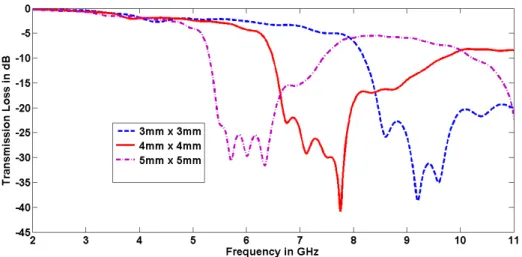
EBG and its equivalent circuit model. Fig. 2 shows the variation of the transmission response of the
mushroom type EBG with different unit element (patch) sizes. The gap between the unit elements is
taken as 1 mm, the via diameter 0.6 mm and the substrate thickness is 0.8 mm. It can be seen from
figure that as the patch size increases, the stop band shifts towards the lower frequency side and this is
due to an increase in the capacitance value. For a mushroom type EBG, the value of capacitance ‘C’, inductance ‘L’ and resonance frequency are given by (1), (2) and (3) respectively [2].
(
)
[ (
) (
) ]
√
Here ‘W’ is the side length of the patch, ‘g’ is the gap between the unit elements, ‘h’ is the thickness of the substrate, ‘r’ is the radius of the via, is the permittivity of free space and is the relative permittivity.
(a) (b)
Fig. 2, Simulated transmission response of Mushroom type EBG for different element size (Substrate thickness=0.8 mm, via diameter =0.6 mm, Gap between unit elements=1 mm)
B. Cross Hair Type EBG
Fig. (3a) shows a cross hair type EBG. It is made by modification of the mushroom type EBG. It
consists of a patch and a number of microstrip lines. The microstrip lines provide extra inductance as
compared to the mushroom type EBG. The diameter of the via is 0.6 mm.The transmission response
of this EBG depends upon the width of the microstrip lines and gap between the unit elements. Fig.
(3b) shows the variation of the transmission response of a cross hair type EBG for different widths of
the microstrip lines used. As the width increases, the resonance frequency shifts towards the higher
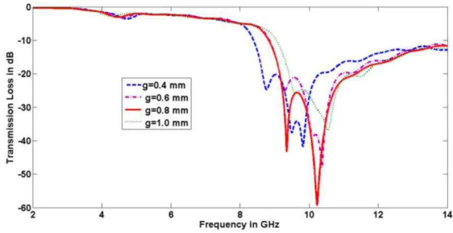
frequency side due to a decrease in the inductance value. Fig. 4 shows the effect of the variation of the
gap ‘g’ between the unit elements on the transmission response of the cross hair EBG. As the gap
decreases the stop band shifts towards the lower end due to an increase in the capacitance value. For
the maximum bandwidth, the gap is optimized and found to be 0.8 mm.
(a) (b)
Fig. 4, Effect of variation of gap between the unit elements ‘g’ on the transmission response (w=0.2 mm, Unit element size=3 mm x 3 mm)
Fig. 5 shows the effect of the unit element size on the transmission characteristics. It can be seen
from the figure that as the unit element size increases, the stop band shifts towards the lower
frequency side due to an increase in the capacitance.
Fig. 5, Effect of unit element size on the transmission response (W=0.2 mm, g=0.8 mm)
C. Swastika type EBG
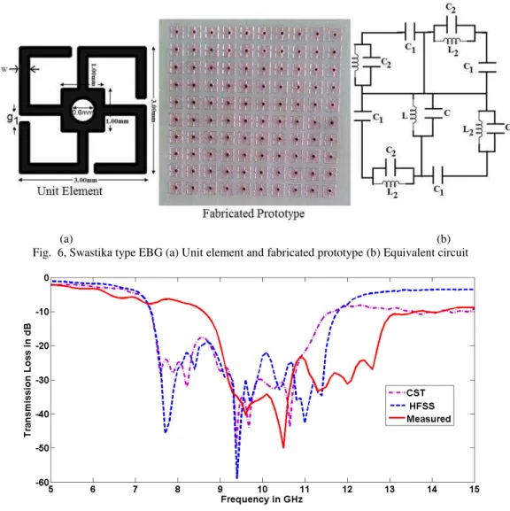
The swastika type EBG is made by introducing a discontinuity in the cross hair type EBG. The
discontinuity in the cross hair type introduces capacitance; hence better resonance is obtained than
cross hair. Fig. (6a) shows a unit element of the swastika type EBG along with the fabricated
prototype while Fig. (6b) shows the equivalent circuit. The inductor L is due to the via and capacitor
C is due to the dielectric between the centre patch and the ground. The inductor L2 is due to microstrip
lines connected with the centre patch and the capacitance C2 is due to the dielectric between the
microstrip line and ground. The capacitor C1 is due to the gap between the two outer microstrip lines.
The swastika type EBG is made on the same substrate (FR-4) as used for the standard mushroom type
EBG. The diameter of via is again taken as 0.6 mm. Fig. 7 shows the measured and simulated
shifted towards the higher frequency side; it is due to the fabrication constraint which keeps a little air
gap between the EBG and the 50 ohm line and this air gap shifts the band towards the higher side.The
swastika type EBG has better transmission response and larger bandwidth than the above two EBGs
(Mushroom and Cross hair).
(a) (b) Fig. 6, Swastika type EBG (a) Unit element and fabricated prototype (b) Equivalent circuit
Fig. 7, Measured and simulated transmission response of the Swastika type EBG
Fig. 8 shows the effect of variation of the strip width g1 on the transmission response. It can be seen
from the figure that as g1 increases, the resonance frequency shifts towards the higher frequency side
due to decrease in the capacitance value. It is also observed that as gap g1 increases, the bandwidth
increases (if -15dB bandwidth is considered). Fig. 9 shows the effect of via diameter variation on the
transmission response of swastika type EBG. It can seen from the figure that as the via diameter
increases, the stop band shifts towards the higher frequency side this is due to a decrease in the via
Fig. 8, Effect of variation of gap between the strips ‘g1’ on transmission response of Swastika type EBG (with w = 0.2 mm
and s= 1 mm).
Fig. 9, Effect of via diameter variation on transmission response of Swastika type EBG
Fig. 11 shows a comparison of the simulated transmission responses of the above discussed three EBGs. It can be seen from the figure that the swastika type EBG has the lowest frequency of operation and highest bandwidth. The Cross Hair type EBG has advantage of lower frequency of operation when compared to the mushroom type EBG.
D. Hexagonal patch type EBG
A hexagonal patch has been selected instead of the rectangular patch used in case of mushroom type
EBG. The hexagonal patch has a side length of 4 mm and the diameter of via used is 1.0 mm. FR-4 is
used for the substrate having thickness of 1.53 mm. Fig. 10 (a) shows the fabricated prototype of the
hexagonal patch EBG. Figure. 10(b) shows the measured and simulated transmission response of the
hexagonal patch EBG. The measured bandwidth obtained is 1 GHz (3.65 GHz to 4.65 GHz).
(a) (b)
Fig. 10, Hexagonal patch type EBG (a) fabricated prototype and (b) Measured and Simulated transmission response.
Table 1 shows the comparison of the -20 dB cut-off frequencies and bandwidths of single band
EBGs. The variation with unit element size for mushroom type EBG and cross hair EBG is also given.
From the comparison, it can be concluded that the Swastika type EBG has better performance in terms
of bandwidth and compactness.
Table – 1, Comparison of simulated cut-off frequencies and bandwidths of different EBGs for single band
S. No. Type of EBG Lower cut-off frequency (GHz)
Higher cut-off frequency (GHz)
Bandwidth (GHz)
1 Mushroom 3 mm x 3 mm 8.50 10.50 2.00
4 mm x 4 mm 6.64 7.96 1.32
5 mm x 5 mm 5.44 6.56 1.12
2 Cross Hair 3 mm x 3 mm 9.10 11.38 2.28
4 mm x 4 mm 6.18 7.36 1.18
5 mm x 5 mm 5.00 6.00 1.00
3 Swastika (3 mm x 3 mm) 7.50 11.10 3.60
4 Hexagonal patch (8 mm x 8 mm)
3.26 4.93 1.67
III. DUAL BAND EBG
The microstrip circuit is periodic in nature, so the response of the circuit repeats after a certain
frequency. This property can be utilized to develop a dual band EBG. Although all the EBG structures
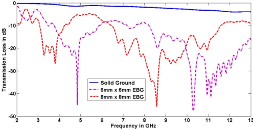
the transmission characteristic of solid ground is shown in Fig. 11. Two different sizes for the
mushroom type EBG (8 mm x 8mm and 6 mm x 6mm) are taken for the purpose. The substrate has
thickness 1.53 mm, via diameter is 1 mm and the gap between the unit elements is 1 mm. It can be
seen from the figure that there is very less attenuation of surface waves in case of solid ground in
comparison to the EBGs. It can also be seen from the figure that as the size of the EBG increases, the
bands shift towards the lower frequency side due to increase in the capacitance.
Fig. 11, Comparison of Simulated transmission response of solid ground and mushroom type EBGs of different size (Substrate thickness=1.53 mm, via diameter=1 mm, Gap between unit elements=1 mm)
A. Hexagonal patch with Double C Type Slot EBG
Fig. 12 (a) shows the ‘C’ type slot EBG and Fig. 12(b) shows the transmission responses for
different slot widths. It can be seen by comparing Fig. 10(b) and Fig. 12 (b) that by cutting ‘C’ type
slot in the hexagonal patch, the stop band shifts towards the lower frequency side. Also, an additional
stop band appears below 10 GHz. This is due to introduction of extra inductance caused by cutting the
slot. It can be seen from Fig. 12(b) that as the slot width increases the band shifts towards the lower
(a) (b)
Fig. 12, Hexagonal patch with C type slot EBG (a) Unit element (b) Transmission response for different slot width.
B. Square patch with a single disconnected loop type slot EBG
Fig. 13(a) shows the unit element of a square patch with a single disconnected loop type slot EBG.
Cutting a slot in the patch introduces extra inductance and hence it shifts the bands towards the lower
frequency side. Fig. 13(b) shows the measured and simulated transmission response of the EBG. Fig.
14 shows the effect of slot width on the transmission response of the EBG. It can be seen from Fig.
14 that as the slot width increases, the lower band shifts towards the lower frequency side
.
(a) (b)
Fig. 14, Effect of slot width on transmission response of Square patch with single disconnected loop type slot EBG
Fig. 15 shows the current distribution of the disconnected loop type slot EBG. The red colour
shows the maximum current density while the blue colour shows the minimum current density. From
the figure, it can be seen that at 3.6 GHz and 8.0 GHz (stop band frequencies of EBG), the signal is
attenuated as it travels from one port to the other. At 6.0 GHz, the signal is not attenuated. It is also
noticed that the attenuation at 8.0 GHz is greater than the attenuation at 3.6 GHz. The higher
attenuation in the upper band is also indicated by a smaller value of S21 in the transmission response
(Fig 14).
Fig. 15, Current distribution of square patch with single disconnected loop type slot EBG at different frequencies.
C. Fractal type EBG
A fractal type EBG having unit element dimensions 6 mm x 6 mm is designed. Fig. 16 shows the
unit element of the fractal type EBG and the comparison of the transmission response of fractal type
EBG with conventional mushroom type EBG having equal unit element size. It can be seen from the
figure that the fractal type EBG has better stop band characteristic than conventional EBG. The
response of the EBG. It can be seen from Fig. 17 that as the patch width decreases, the higher
frequency band shifts towards thehigher side and after a particular value of slot width the band splits.
The optimum value of slot width is found to be 1.4 mm. There is no effect of slot width variation on
the lower frequency band. Fig. 18 shows the effect of gap between unit elements. It can be seen from
Fig. 18 that as the gap increases, the band shifts towards the higher frequency side due to decrease in
the capacitance. It is noticed that the bandwidth of the higher band depends also on ‘g’. The optimum value of ‘g’ is found to be 0.8 mm.
(a) (b)
Fig. 16, Fractal type EBG (a) Unit element (b) Transmission response comparison of fractal and conventional mushroom type element having equal unit element size
Fig. 18, Effect of gap ‘g’ variation between unit elements on transmission response of the fractal EBG (x = 2 mm, y = 1.4 mm, a = b = 0.6 mm)
Table 2 shows the comparison of the -20 dB cut-off frequencies and bandwidths of the different
dual band EBGs. From the comparison, it can be concluded that cutting a slot shifts the band towards
the lower frequency side hence compactness can be achieved. Fractal type EBG offers nearly the
same cut-off frequency and bandwidth for the lower band as the mushroom type EBG of same size.
However, it offers a large bandwidth for the upper band in comparison to mushroom type EBG. From
the table, it can be concluded that rectangular patch with a single disconnected loop type slot EBG is
more compact while fractal type EBG has larger bandwidth.
Table – 2, Comparison of simulated cut-off frequencies and bandwidths of different EBGs for dual band
S. No.
Type of EBG Lower Band Higher Band
Lower cut-off Freq. (GHz) Higher cut-off Freq. (GHz) Bandwidth (GHz) Lower cut-off Freq. (GHz) Higher cut-off Freq. (GHz) Bandwidth (GHz)
1 Mush- room
6 mm x 6 mm
4.22 4.95 0.73 9.92 12.60 2.68
8 mm x 8 mm
3.23 3.87 0.65 7.74 9.95 2.21
2 Hexagonal patch with Double C Type Slot(8 mm x 8 mm)
2.74 3.75 1.01 6.60 8.63 2.03
3 Square patch with a single disconnected loop type slot
(6 mm x 6 mm)
3.11 3.77 0.66 7.28 9.25 1.97
4 Fractal EBG (6 mm x 6mm)
IV. CONCLUSIONS
Different types of Electromagnetic Band Gap Structures for single and dual band operation in the
FCC UWB region are investigated. The effects of the unit element size, gap between the unit elements
and via diameter on the transmission response of the EBGs are studied. As the unit size increases, the
stop bands shift towards the lower frequency side due to an increase in the capacitance. Increase in the
gap between the unit elements shifts the stop bands towards higher frequency side due to decrease in
the capacitance. Increase in the via diameter shifts the stop bands towards higher frequency side due
to decrease in inductance. Among the single band EBGs, the swastika type EBG is seen to offer better
performance in terms of both compactness (lower resonance frequency) and bandwidth. Among the
dual band EBGs, the square patch with a single disconnected loop type slot EBG offers better
performance in terms of compactness while the fractal type EBG offers better performance in terms of
bandwidth. The proposed EBGs will have applications such as enhancement of antenna gain and
bandwidth, signal integrity enhancement and noise reduction for filters, reduction of mutual coupling
for antenna arrays and suppression of noise in high speed switching circuits.
V.ACKNOWLEDGEMENT
The author likes to acknowledge vice chancellor DIAT (DU), for financial support. Author also likes to acknowledge R. V. S. Rama Krishna for his technical suggestions.
REFERENCES
[1] D. Sievenpiper, “High-impedance Electromagnetic Surfaces”, Ph. D. dissertation, Department of Electrical Engineering, University of California at Los Angeles, Los Angeles, CA, 1999.
[2] Fan Yang and Yahya Rahmat Samii, ”Electromagnetic Band Gap Structures in Antenna Engineering”, Cambridge university press 2009.
[3] Y. Lee, J. Yeo, K. Ko, Y. Lee, W. Park, and R. Mittra, “A novel design technique for control of defect frequencies of an electromagnetic band gap (EBG) cover for dual band directivity enhancement”, Microw. Opt. Technol. Lett., vol. 42, no. 1, pp. 25–31, Jul. 2004.
[4] A. Pirhadi, F. Keshmiri, M. Hakkak and M. Tayarani, “Analysis and Design of Dual Band High Directive EBG Resonator Antenna Using Square Loop FSS as Superstrate Layer”, Progress In Electromagnetics Research PIER, vol. 70, pp.1-20, 2007.
[5] D. Sievenpiper, L. Zhang, R.F. Jimenez Broas, N. G. Alexopoulos, and E. Yablonovitch, “High-impedance electromagnetic surfaces with a forbidden frequency band”, IEEE Trans. Microwave Theory Techn., vol.47, pp. 2059 -2074, Nov. 1999.
[6] Li Yang; Mingyan Fan; Fanglu Chen; Jingzhao She; ZhengheFeng, "A novel compact electromagnetic-bandgap (EBG) structure and its applications for microwave circuits", Microwave Theory and Techniques, IEEE Transactions on , vol.53, no.1, pp.183-190, Jan. 2005.
[7] Sai Wai Wong; Lei Zhu, "EBG-Embedded Multiple-Mode Resonator for UWB Band Pass Filter With Improved Upper-Stop band Performance”, Microwave and Wireless Components Letters, IEEE , vol.17, no.6, pp.421,423, June 2007. [8] J. F. Frigon, C. Caloz, and Y. Zhao, “Dynamic radiation pattern diversity (DRPD) MIMO using CRLH leaky-wave
antennas”, Proc. IEEE Radio Wireless Symp., Jan. 2008, pp. 635–638.
[9] P. N. Fletcher, M. Dean, and A. R. Nix, “Mutual coupling in multi element array antennas and its influence on MIMO channel capacity”, Electron. Lett., vol. 39, pp. 342–344, Feb. 2003.
[10] Payandehjoo, Kasra and Abhari Ramesh, “Employing EBG Structures in Multiantenna Systems for Improving Isolation and Diversity Gain”, IEEE Antennas and Wireless Propagation Letters, vol. 8, pp. 1162-1165,2009.
[11] Mohamad Yajdi and Nader Komjani, ‘Design of a band notched Ultra wideband antenna by means of EBG structure”, IEEE Antenna propagation letters, VOL. 10, pp. 170-173, 2011.
[17] S. Shahparnia, Ramahi, M. Omar, "A simple and effective model for electromagnetic bandgap structures embedded in printed circuit boards", Microwave and Wireless Components Letters, IEEE , vol.15, no.10, pp.621,623, Oct. 2005. [18] Elek, Francis, G.V. Eleftheriades, "Dispersion analysis of the shielded Sievenpiper structure using multiconductor
transmission-line theory", Microwave and Wireless Components Letters, IEEE , vol.14, no.9, pp.434,436, Sept. 2004. [19] L. Peng, C. L. Ruan, and J. Xiong. “Compact EBG for multi-band applications”IEEE Transactions on Antennas and
Propagation, vol. 60, pp. 4440-4444, 2012.
[20] X. L. Bao, G. Ruvio, and M. J. Ammann, “Low-profile dual-frequency GPS patch antenna enhanced with dual-band EBG structure,” Microw. Opt. Technol. Lett., vol. 49, no. 11, pp. 2630,-2634, Nov. 2007.
[21] T. Kamgaing, and O. M. Ramahi, “Multiband Electromagnetic-Bandgap Structures for Applications in Small Form-Factor Multichip Module Packages,” IEEE Trans. Microw. Theory Tech., vol. 56, no. 10, pp. 2293-2300, Oct. 2008. [22] Lin Peng; Cheng-Li Ruan; Li, Zhi-Qiang, "A Novel Compact and Polarization-Dependent Mushroom-Type EBG Using