Abstract— This paper discusses how symbolic computation combined with a circuit model can be used for analyzing planar multilayer structures, in a manner suitable for educational approach. Working in the Fourier domain, expressions for the transversal spectral Green’s functions are evaluated in compact, closed form using the symbolic computation capability of the Mathematica package. Printed antennas were analyzed through the method of moments. Further validation was achieved with the IE3D and HFSS packages.
Index Terms—Planar multilayer structures, spectral fields, Green’s functions, circuit model, method of moments, education.
I. INTRODUCTION
Sources positioned on the interfaces of planar multilayer structures can be used as a practical model in
a wide variety of applications such as geophysical investigations, remote sensing, optoelectronics,
microwaves, military surveillance and antenna theory [1], [2]. For accurate results, the analysis of these
structures requires numerical methods such as the Method of Moments (MoM), Finite Elements or
Finite Differences. It is presently widely accepted that MoM-based algorithms are suitable for
rigorous numerical analysis of printed structures of small to medium sizes (in terms of wavelength)
stacked up in layers [1]. However, for the application of this method, either in the spectral or in the
spatial domain, the corresponding Green’s functions need be derived. Due to their complex
calculations, an essential question is posed: which is the most proper approach for determining the
entire set of Green’s functions, particularly for educational purposes?
In the spatial domain, Green’s functions for multilayer media are traditionally represented by
Sommerfeld’s integrals. Due to the oscillatory nature of these integrals, their numerical computation is
inefficient and time-consuming [1]. Consequently, this approach is not recommended for a first
graduate course on applied electromagnetism. On the other hand, spectral Green’s functions can be derived
in closed form if appropriate techniques are utilized [3]-[5]. However, the calculations of spectral fields in
multilayer structures are usually tedious and error-prone if done by hand, what is especially true in the
analysis of structures with anisotropic and bi-isotropic materials [6], [7].
Planar Multilayer Structure Analysis: an
Educational Approach
D.B. Ferreira
Fundação Centro de Pesquisa e Desenvolvimento em Telecomunicações – CPqD Rodovia Campinas – Mogi-Mirim, km 118,5
13086-902 Campinas – SP, Brazil [email protected]
A.F. Tinoco Salazar, I. Bianchi, and J.C. da S. Lacava Laboratório de Antenas e Propagação,
Instituto Tecnológico de Aeronáutica, Pr. Mal. Eduardo Gomes 50,
To overcome this limitation, this paper presents a new elegant procedure for calculating the
electromagnetic fields in multilayer structures. Using the full-wave equivalent circuit, first established by
Dreher in [8], and the symbolic computation capability of the Mathematica package [9], expressions for
the transformed electromagnetic fields are derived in a straightforward, error-free way. Consequently, the
corresponding spectral Green’s functions can be determined in compact, closed form, with considerable
reduction of the calculation time. Based on this procedure, a method-of-moments (MoM) algorithm was
implemented in Mathematica with the purpose of analyzing printed antennas. The results confirm the
usefulness of the new procedure, which can also be applied to more complex structures and substrates, like
in the anisotropic and bi-isotropic cases. Furthermore, the implemented algorithm can be utilized in a
microstrip antenna course for engineering students, since it allows for the fast evaluation of electrical and
geometrical effects on the antenna parameters.
II. THEORY
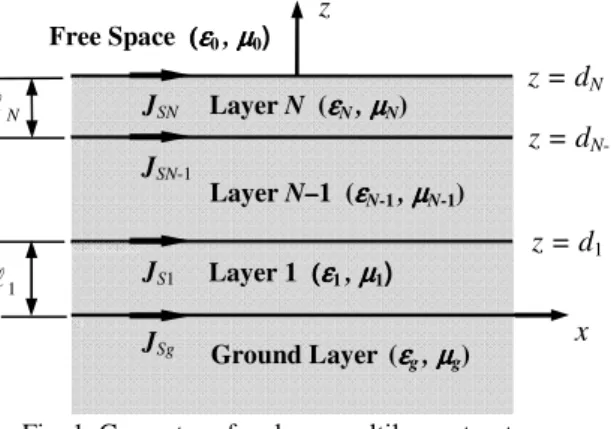
A planar multilayer structure composed of N + 2 isotropic, linear and homogenous layers stacked up in
the z direction is shown in Fig. 1. The layers are assumed to be unbounded along the x and y directions.
Fig. 1. Geometry of a planar multilayer structure.
The lower layer, having complex permittivity εg and complex permeability g, is denoted the ground
layer and occupies the negative-z region. The next N layers are characterized by thickness ℓn, complex
permittivity εn and complex permeability n, where 1 ≤n≤N. The planar interface z = dN separates the
N-th layer from free space (the upper layer). Metallic patches are printed at arbitrary positions on each one
of the N + 1 interfaces of the structure. The surface current densities on these elements are given by
JSξ(x, y)=x JSξ x(x, y)+y JSξ y(x, y) - (ξ ∈ {g, n}), where boldface letters represent vectors, and x and y are
the unit vectors along the x- and the y-directions, respectively. These current densities are considered the
virtual sources of the electromagnetic field within each layer. Since the layers are free of sources (the
sources are located on the interfaces of the multilayer structure, as depicted in Fig. 1), the electric field in
the spatial domain of a monochromatic wave can be written, according to spectral techniques, as a
superposition of plane waves, as follows [10]
∫ ∫
∞∞ −
∞
∞ −
+ −
= kx ky z e i k x k y dkxdky z
y
x ( x y )
2 ( , , )
4 1 ) , ,
( E
π
E , (1)
where the function E (kx,ky,z) is the spectral electric field, and kx and ky are the spectral variables. 1
ℓ
Layer N−−−−1 (εεεεN-1, µµµµN-1) Layer N (εεεεN , µµµµN)
z
JSN
JSN-1
Ground Layer (εεεεg , µµµµg) Layer 1 ((((εεεε1, µµµµ1)
JS1
JSg x
z = d1 z = dN-1
z = dN
Free Space ((((εεεε0, µµµµ0)
N
For the n-th confined layer, located between the interfaces z = dn-1 and z=dn, the spectral fields En (kx,ky,z)
and Hn (kx,ky,z) can be written as the superposition of two plane waves traveling in the ± z directions, that is
∑
= =
2
1
) , ( )
, , (
τ
τ x y ik τz
n y
x
n k k z e k k e nz
E , (2)
∑
= =
2
1
) , ( )
, , (
τ
τ x y ik τz
n y
x
n k k z h k k e nz
H , (3)
where enτ(kx,ky) and hnτ(kx,ky) are the amplitudes of the spectral fields, knzτ = (−1)τ(ω2µnεn−u
2
)1/2 and
2 2 2
y
x k
k
u = + . Since the propagation function is given by eiknzτz for the n-th confined layer then, for a
plane wave traveling in the +z direction, the square root in the propagation constant knz1 needs to be
adequately evaluated; in this case, Re{knz1}≤0 and Im{knz1}≥0. Similarly, for the plane wave traveling in
the –z direction, the square root in knz2 is calculated considering that Re{knz2}≥0 and Im{knz2}≤0. With
these restrictions on the signs of the real and imaginary parts of knzτ, Sommerfeld’s radiation condition [14]
is satisfied.
From Maxwell’s equations and using the symbolic computation capability of the Mathematica
package, the amplitudes of the spectral fields in the x and y directions (enxτ, enyτ, hnxτ, and hnyτ, with
τ = 1 or 2) can be expressed in terms of the field amplitudes in the z direction, enzτ and hnzτ, according
to [5]. They are listed below and the Mathematica command lines utilized for their determination are
given in the Appendix.
) h e
(
enxτ =u−2 kxknzτ nzτ −ωµnky nzτ , (4)
) h e
(
enyτ =u−2 kyknzτ nzτ +ωµnkx nzτ , (5)
) h e
(
hnxτ =u−2 kyωεn nzτ +kxknzτ nzτ , (6)
) h e
(
hnyτ =u−2 −kxωεn nzτ +kyknzτ nzτ . (7)
In order to establish the full-wave equivalent circuit for the n-th layer, firstly the x- and y-component of
the spectral fields, given by equations (2)-(3), are specified at the z = dn interface, producing the following
set of four equations in the unknown amplitudes enzτ and hnzτ
∑
=
− −
=
2
1
2 ( e h )
) , , (
τ
τ τ
τ nz ωµn y nz iknzτdn nz
x n
y x
nx k k d u k k k e
E , (8)
∑
=
− +
=
2
1 2
) h e
( )
, , (
τ
τ τ
τ nz ωµn x nz iknzτdn nz
y n
y x
ny k k d u k k k e
E , (9)
∑
=
− +
=
2
1
2 ( e h )
) , , (
τ
τ τ
τ τ
ωε iknz dn
nz nz x nz n y n
y x
nx k k d u k k k e
∑
= − − + = 2 1 2 ) h e ( ) , , ( τ τ τ τ τωε iknz dn
nz nz y nz n x n y x
ny k k d u k k k e
H . (11)
Solving this system (equations (8)–(11)), expressions for en zτ and h n zτ, in terms of Enx (kx,ky,dn),
Eny (kx,ky,dn), Hnx (kx,ky,dn), and Hny (kx,ky,dn) are obtained. Then, replacing these expressions in the same
set of transversal components given by equations (2)-(3), but now specified at z = dn-1, results in the
following relationship between the transversal components of the spectral fields (t∈ {x, y}) at the upper and the lower interfaces of the n-th layer
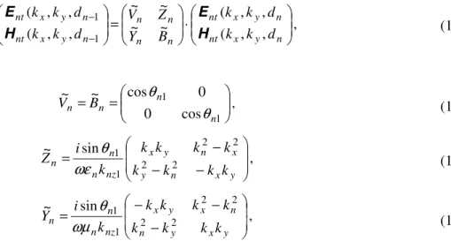
⋅ = − − n y x nt n y x nt n n n n n y x nt n y x nt d k k d k k B Y Z V d k k d k k , , ( , , ( ~ ~ ~ ~ , , ( , , ( 1 1 H E H E
, (12)
where = = 1 1 cos 0 0 cos ~ ~ n n n n B V θ θ
, (13)
− − − = y x n y x n y x nz n n n k k k k k k k k k i
Z 2 2
2 2 1 1 sin ~ ωε θ
, (14)
− − − = y x y n n x y x nz n n n k k k k k k k k k i
Y 2 2
2 2 1 1 sin ~ ωµ θ
, (15)
with θn1 = knz1ℓn and kn2 =ω2µnεn. Again, symbolic computation was performed in the Mathematica
package. As an example, the calculation of the first row of the matrix Z~n is given in the Appendix. Consequently, for the n-th confined layer, a two-port full-wave equivalent circuit, as shown in Fig. 2,
can be established.
n n n n V Z Y B ɶ ɶ ɶ ɶ 1 ( )
nt dn−
E ( )
nt dn
E 1
( )
nt dn−
H ( )
nt dn
H n n n n V Z Y B ɶ ɶ ɶ ɶ 1 ( )
nt dn−
E ( )
nt dn
E 1
( )
nt dn−
H ( )
nt dn
H
Fig. 2. Full-wave equivalent circuit.
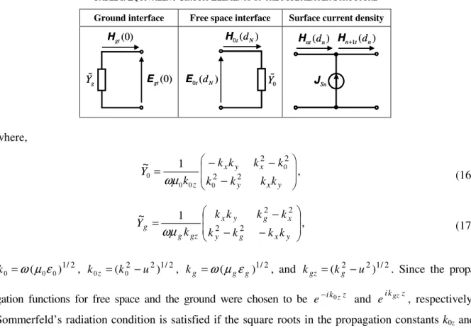
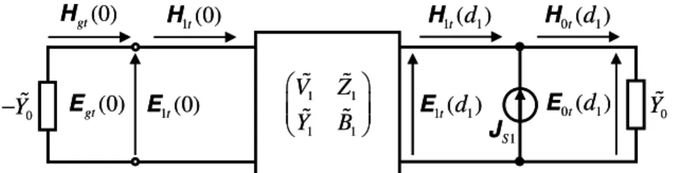
An equivalent procedure is employed to evaluate the fields at the free space and the ground layer
interfaces. The boundary conditions are then applied for the planar interfaces, resulting in the circuit
elements shown in Table I. Then, the multilayer structure depicted in Fig. 1 can be modeled by the
circuit illustrated in Fig. 3.
(0) gt H
ɶ g
Y 1 1
1 1 V Z Y B ɶ ɶ ɶ ɶ
1t(0)
H 1( )1
t d H
1
S J
0t(dN) H 0 ɶ Y
...
...
N N N N V Z Y B ɶ ɶ ɶ ɶ 1 ( )Nt dN−
H HNt(dN)
SN J
1
S N−
J Sg J (0) gt H ɶ g
Y 1 1
1 1 V Z Y B ɶ ɶ ɶ ɶ
1t(0)
H H1t( )d1
1
S J
0t(dN) H 0 ɶ Y
...
...
N N N N V Z Y B ɶ ɶ ɶ ɶ 1 ( )Nt dN−
H HNt(dN)
SN J
1
S N−
J Sg
J
TABLE I.EQUIVALENT CIRCUIT ELEMENTS OF THE MULTILAYER STRUCTURE
Ground interface Free space interface Surface current density
(0) gt E (0) gt H
ɶ g
Y Egt(0) (0)
gt H
ɶ g
Y E0t(dN)
0t(dN) H
0 ɶ Y 0t(dN)
E
0t(dN) H
0 ɶ Y
( ) nt dn H
1( )
n+t dn H
Sn J ( ) nt dn H
1( )
n+t dn H
Sn J
where,
−
− −
=
y x y
x y x
z k k k k
k k k k
k
Y 2 2
2 2
0
0 0
0 0
1 ~
ωµ , (16)
− −
− =
y x g y
x g y x gz g g
k k k k
k k k k
k
Y 2 2
2 2
1 ~
ωµ , (17)
2 / 1
) ( 0 0 0 =ω µ ε
k , k0z =(k02 −u2)1/2,
2 / 1
) ( g g
g
k =ω µ ε , and kgz =(kg2−u2)1/2. Since the propa
gation functions for free space and the ground were chosen to be e−ik0zz and eikgzz, respectively,
Sommerfeld’s radiation condition is satisfied if the square roots in the propagation constants k0z and
kgz are calculated as follows: Re{k0z}≥0, Im{ k0z}≤0, Re{kgz}≥0 and Im{kgz}≤0.
Before finishing this section, it is important to point out that the theory developed here can also be
applied to planar multilayer structures where the metallic patches are positioned inside the confined layers.
For these cases, the metallic patch can simply be considered to be at the interface between two adjacent layers
having the same electrical characteristics. Hence, the developed theory can be utilized without any change.
III. APPLICATIONS
As a first application, a printed Yagi-Uda antenna fed by a delta-gap generator was investigated. In this
case, the multilayer structure, shown in Fig. 4, is composed of the free space–substrate–free space layers.
1 d
x
y z
1 L
2 L
a
1
2w 2w2
1 0
(ε , µ )
1 d
x
y z
1 L
2 L
a
1
2w 2w2
1 0
(ε , µ )
Fig. 4. Geometry of a Yagi-Uda antenna excited by a delta-gap generator.
The radiator consists of two narrow flat dipoles printed on the dielectric substrate of thickness d1,
respectively by L1 and 2w1 (L1>> 2w1), for the driven element, and L2 and 2w2 (L2>> 2w2), for the
parasitic one. The distance between elements is a. The transversal Green’s functions at the antenna
interface z = d1 are easily computed from the circuit model depicted in Fig. 5, as follows
1 1 1 1 1 1 1 1 1 1 )] ~ ~ ~ ( ) ~ ~ ~ ( ~ ( ) , , ( ) , , ( ) , , ( ) , , ( 0 0 0 − − ⋅ + ⋅ ⋅ + + = − − V Y Y Z Y B Y d k k G d k k G d k k G d k k G y x yx y x yy y x xx y x xy
, (18)
where )] 2 ( [ { ) ( cos ) ( 2 ) , ,
( x y 1 = 0
{
12z1 0z x2 − 02 r1 2 11 − 1z1 02z 02z r1+ 12z1 r1+xx k k d k k k k ik k k k
G η ε θ ε ε
) ( { ) ( sin ) cos( )]} 1 2 (
[ 121 2 1 11 11 121 121 2
2
0 0
0z r z z z z
z
y k k k k k k
k + + + +
+ ε θ θ
) /( ) ( sin ]} ) 2 (
[ 121 1 2 1 2 11 11 21
2
0
0
}
k T Tk k
ky z −εr + zεr θ
+ , (19)
) ( sin ) cos( )] 1 2 ( [ ) ( cos 2 { ) , ,
( x y 1 =η0 x y 12z1 0zεr1 2 θ11 + 1z1 12z1 + 02z εr1+ θ11 θ11
xy k k d k k k k ik k k
G ) /( ) ( sin ] ) 2 (
[ 121 1 02 1 2 11 0 11 21
0 k k
}
k T Tk z z −εr + zεr θ
− , (20)
) , , ( ) , ,
(k k d1 G k k d1
Gyy x y = xx y x , (21)
) , , ( ) , ,
(k k d1 G k k d1
Gyx x y = xy x y , (22)
) ( sin ) ( ) ( cos
2 11 11 121 2 11
11 k z k0z θ i k z k0z θ
T = + + , (23)
) ( sin ) ( ) ( cos
2 11 1 11 121 2 21 11
21 k z k0zεr θ i k z k0zεr θ
T = + + , (24)
η0 is the intrinsic impedance of free space and εr1 is the relative electric permittivity of the substrate.
Notice that the transversal Green’s functions in (19) to (22) are equivalent to the ones presented in
[16], where they were evaluated analytically, i.e., without employing a full-wave equivalent circuit to
represent the planar multilayer structure.
1t(0)
E
1t( )d1 E 1t(0)
H
1t( )d1 H
1
S
J
0t(d1) E
0
ɶ
Y 0t( )d1 H 1 1 1 1 ɶ ɶ ɶ ɶ V Z Y B (0) gt E (0) gt H 0 Y
−ɶ E1t(0) E1t( )d1
1t(0)
H
1t( )d1 H
1
S
J
0t( )d1 E
0
ɶ
Y 0t( )d1 H 1 1 1 1 ɶ ɶ ɶ ɶ V Z Y B (0) gt E (0) gt H 0 Y −ɶ
Fig. 5. Full-wave equivalent circuit for the structure depicted in Fig. 4.
Once the Green’s functions are derived, the next step is to determine the Yagi antenna’s electric
characteristics, such as its input impedance and radiation pattern. This involves solving integral
equations constrained by the pertinent boundary conditions. In the present case, the following
equations are obtained by enforcing the tangential electric field component being zero on the perfect
conducting surface of the antenna elements,
0 ) , ( ) , , ( 1
0 x y d +E x y =
E x f , on the driven element (25)
0 ) , ,
( 1
0 x y d =
E x , on the parasitic element (26)
Lv >> 2wv, (v∈ {1, 2}), the unknown consists of just the x-components of the surface current densities
Jxv(x, y) excited on the dipoles.
Using the MoM procedure - the most widely utilized numerical technique for rigorous analysis of
printed geometries on multilayer planar media - to solve the system of equations (25)-(26), the electric
current densities Jxv(x, y) are expanded in a set of basis-functions as follows,
x
J ( , ) ( , )
1
1 1
1 x y I J x y
M m m x m x
∑
== , on the driven element (27)
x
J ( , ) ( , )
1
2 2
2 x y I J x y
N n n x n x
∑
== , on the parasitic element (28)
where Jx1m and Jx2n are the basis-functions, and Ix1m and Ix2n are coefficients to be determined.
After applying Galerkin method [11] and Parseval’s theorem [12], the following linear system is
established
(
)
( )
(
)
( )
(
(
)
)
( )
= ⋅ × × × × × × × × 1 1 1 2 1 1 ) 0 ( N M p N n x M m x N N qn M N qm N M pn M M pm V I I Z Z Z Z, (29)
where y x y x * p x y x m x y x xx
pm G k k d k k k k dk dk
Z ( , , ) ( , ) ( , )
4 1
1 1
1
2
∫ ∫
J J+∞ ∞ − +∞ ∞ − − =
π , (30)
y x y x * p x y x n x y x xx
pn G k k d k k k k dk dk
Z ( , , ) ( , ) ( , )
4 1
1 2
1
2
∫ ∫
J J+∞ ∞ − +∞ ∞ − − =
π , (31)
y x y x * q x y x m x y x xx
qm G k k d k k k k dk dk
Z
∫ ∫
( , , 1)J 1 ( , )J 2 ( , ) +∞ ∞ − +∞ ∞ −= , (32)
y x y x * q x y x x y x xx
qn G k k d k k k k dk dk
Z
∫ ∫
( , , 1)J 2n( , )J 2 ( , ) +∞ ∞ − +∞ ∞ −= , (33)
∫
= 1 ) , ( ) ,( *1
S
p x f
p E x y J x y dS
V , (34)
Jxv(kx,ky) is the Fourier transform of Jxv(x, y), S1 is the driven element surface, p = 1, 2, … , M, and
q = 1, 2, … , N.
Piecewise-linear sub-domain rooftop basis-functions (taking into account the edge condition) were
used for expanding the surface current densitiesJxv(x, y), so that
) ( ) ( ) ,
(x y T x B y
Jxνm = νm ν , (35)
where − − ∆ − ≤∆ = otherwise , 0 if , / 1 )
( ν ν ν ν
ν x x x x x x x
Tm m m (36)
≤ − = − otherwise , 0 if , ) / ( 1 ) ( 1 2 ν ν ν
ν y πw y w y w
∆x1= L1/(M + 1), x1m = –L1/2 + m∆x1, ∆x2= L2/(N + 1), x2n = –L2/2 + n∆x2, and v∈ {1, 2}.
As a delta-gap generator is used to feed the driven element, then
) ( ) ,
(x y E0 x
Ef = δ , y ≤w1 (38)
where δ(x) is the Dirac’s delta function. Consequently, the excitation equation (30) can be rewritten as
= +
=
otherwise ,
0
2 / ) 1 ( if ,
0 p M E
Vp (39)
with M being an odd number.
Using this approach, a Mathematica-based CAD software capable of performing the analysis of printed
antennas was implemented. For greater efficiency in the numerical calculation of the elements Zpm, …, Zqn
of the impedance matrix [Z] (equation (29)), mathematical procedures - like parity analysis of the Green’s
functions, change of the coordinate system (rectangular to polar) and asymptotic extraction technique [13]
- were applied. To illustrate their effect, after changing the coordinate system - (ρ,φ) are the polar
coordinates - and undertaking the parity analysis, equation (30) assumes the simpler form [14]
φ ρ ρ φ ρ φ
ρ φ
ρ π
π
d d d
G
Zpm 12 xx( , , 1) x1m( , ) *x1p( , ) 2
/
0 0
J J
∫ ∫
∞ −= . (40)
For applying the asymptotic extraction technique, first the asymptotic term is calculated, resulting in
) 1 (
) ( cos )
, , (
0
2 1
r xx
i d
G
ε ωε
φ ρ φ
ρ ρ
+ =
∞
→ . (41)
Consequently, Zpm can be evaluated from
φ ρ ρ φ ρ φ
ρ φ
ρ φ
ρ π
π
ρ d d
d G
d G
Zpm 12 [ xx( , , 1) xx( , , 1) ] x1m( , ) *x1p( , ) 2
/
0 0
J J
∫ ∫
∞ − →∞− =
φ ρ φ ρ φ
ρ φ
ρ ε
ωε π
π
d d
i *
p x m
x r
) , ( ) , ( ) ( cos )
1
( 1 1
2 2 2
2 /
0 0 0
J J
∫ ∫
∞ +− . (42)
The first double integral in (42) depends on the operating frequency, whereas the second one does not.
These are the well-known Sommerfeld’s integrals, whose integrands exhibit singularities in the form of
branch points and poles, so that their numerical calculation requires careful attention. The poles, often
complex, correspond to surface and leaky waves that can be excited in the dielectric layer. The number of
poles depends on the thickness of the layer, its electrical permittivity and the wave number. An efficient
way to calculate these integrals is the use of a deformed path of integration, with adaptive routines in the
vicinity of the poles and branch points. Details on the numerical integration can be found in [15] – [17]. In
this work, a triangular path was chosen to calculate the elements Zpm, …, Zqn of the impedance matrix.
Finally, as the antenna is fed directly by a delta-gap generator, it is important to point out that the dielectric
thickness poses no limitation on the application of the present theory.
2 / ) 1 ( 1
/
1 +
= x M
in I
Z , (43)
where E0 was selected as 1 V.
To validate the developed CAD, a Yagi-Uda antenna with L1 = L2 = 56.294 mm, 2w1 = 2w2 = 3.0 mm,
a = 28.174 mm, d1 = 3.048 mm, εr1 = 2.55 and tgδ = 0.0022 (ε1 = εr1ε0 (1 - itgδ)), was analyzed. Fig. 6 shows the
results obtained for the input impedance (M = N = 17) compared to those simulated in two commercial software,
HFSS and IE3D (a MoM-based software).
1.90 1.95 2.00 2.05 2.10
-15 0 15 30 45 60 75
In
p
u
t
im
p
ed
an
ce
[
Ω
]
Frequency [GHz]
Re(Zin) - CAD Im(Zin) - CAD Re(Zin) - HFSS Im(Zin) - HFSS Re(Zin) - IE3D
Im(Zin) - IE3D
Fig. 6. Yagi-Uda input impedance.
The radiation pattern was calculated using the following expressions, derived from the stationary phase
method [14]:
) cos ( 1
1) sin ( , , )] 0 1
, , ( [cos 2
) , (
0 0
θ
θ π φ xx xe ye φ yx xe ye ik r d
ye xe xs
e d k k G d
k k G r
k k k i
E = J + − − , (44)
) cos ( 1
1) cos ( , , )] 0 1
, , ( sin [ cos 2
) , (
0 0
θ
φ π θ φ xx xe ye φ yx xe ye ik r d
ye xe xs
e d k k G d
k k G r
k k k i
E = J − + − − , (45)
where Jxs(kxe,kye) = Jx1(kxe,kye) + Jx2(kxe,kye) and the subscript e denotes the functions are calculated at
the stationary phase point (kxe = k0 sinθ cosφ; kye = k0 sinθ sinφ), for 0 ≤ θ≤ π/2 and 0 ≤ φ< 2π.
Fig. 7 presents the results for the yz-plane radiation pattern calculated at 2.0 GHz.
-40 -30 -20 -10 0
0°
30°
60°
90°
120°
150° 180°
210° 240° 270°
300° 330°
-40
-30
-20
-10
0
CAD
HFSS IE3D
[dB]
The agreement between our results for the input impedance and radiation pattern with those
simulated in HFSS and IE3D certifies the accuracy of the technique presented in this work.
As a second application, the three-layer structure (perfect ground plane – substrate – free space) shown
in Fig. 8 was analyzed.
1 d x y z 1 L 1 2w 1 0 (ε , µ) 1 d x y z 1 L 1 2w 1 0 (ε , µ)
Fig. 8. Geometry of a flat printed dipole excited by a delta-gap generator.
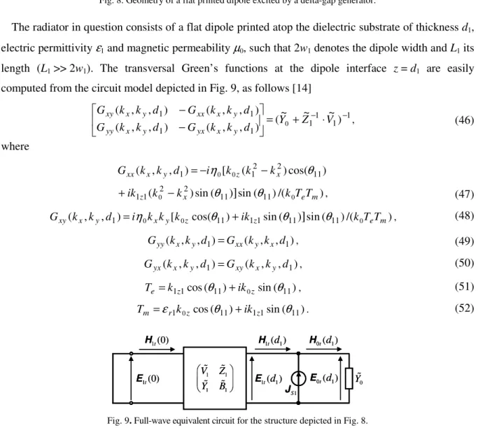
The radiator in question consists of a flat dipole printed atop the dielectric substrate of thickness d1,
electric permittivity ε1 and magnetic permeability µ0, such that 2w1 denotes the dipole width and L1 its
length (L1>> 2w1). The transversal Green’s functions at the dipole interface z = d1 are easily
computed from the circuit model depicted in Fig. 9, as follows [14]
1 1 1 1 1 1 1 1 ) ~ ~ ~ ( ) , , ( ) , , ( ) , , ( ) , , ( 0 − − ⋅ + = − − V Z Y d k k G d k k G d k k G d k k G y x yx y x yy y x xx y x xy
, (46)
where ) cos( ) ( [ ) , ,
( x y 1 η0 0z 12 x2 θ11
xx k k d i k k k
G =− −
) /( ) ( sin ) ( sin )
( 0 11 11 0
2 2 1
1z k kx ] k TeTm
ik − θ θ
+ , (47)
) /( ) ( sin ) ( sin ) cos( [ ) , ,
( x y 1 0 x y 0z 11 1z1 11
]
11 0 e mxy k k d i k k k ik k T T
G = η θ + θ θ , (48)
) , , ( ) , ,
(k k d1 G k k d1
Gyy x y = xx y x , (49)
) , , ( ) , ,
(k k d1 G k k d1
Gyx x y = xy x y , (50)
) ( sin )
(
cos 11 11
1
1z θ 0z θ
e k ik
T = + , (51)
) ( sin )
(
cos 11 11 11
1 0 θ θ
εr z z
m k ik
T = + . (52)
1t(0)
E E1t( )d1
1t(0)
H H1t(d1)
1
S J
0t(d1)
E
0
ɶ
Y 0t(d1)
H 1 1 1 1 ɶ ɶ ɶ ɶ V Z Y B
1t(0)
E E1t(d1)
1t(0)
H H1t(d1)
1
S J
0t(d1)
E
0
ɶ
Y 0t(d1)
H 1 1 1 1 ɶ ɶ ɶ ɶ V Z Y B
Fig. 9. Full-wave equivalent circuit for the structure depicted in Fig. 8.
Once again, the transversal Green’s functions evaluated through the full-wave equivalent circuit
((47) to (50)) are equivalent to the ones analytically calculated in [16], [17].
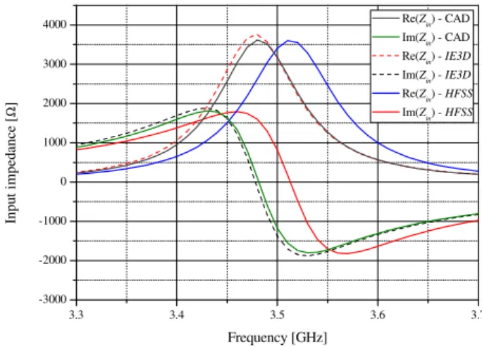
printed on a substrate of εr1 = 2.55, d1 = 3.048 mm, tg δ = 0.0022) are shown in Figs. 10 and 11, respectively.
3.3 3.4 3.5 3.6 3.7
-3000 -2000 -1000 0 1000 2000 3000 4000
In
p
u
t
im
p
ed
an
ce
[
Ω
]
Frequency [GHz]
Re(Zin) - CAD Im(Zin) - CAD Re(Zin) - IE3D Im(Zin) - IE3D
Re(Zin) - HFSS
Im(Zin) - HFSS
Fig. 10. Dipole input impedance.
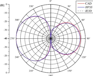
Again, the results for the dipole input impedance and radiation pattern compared with simulations
performed in HFSS and IE3D validate the accuracy of our CAD.
-30 -20 -10 0
0°
30°
60°
90° 270°
300°
330°
-30
[dB] CADIE3D
HFSS
Fig. 11. Dipole radiation patterns plotted at 3.48 GHz: yz plane.
IV. FINAL COMMENTS
In this paper an elegant and efficient approach, based on a full-wave circuit model and employing the
symbolic capability of the Mathematica package, to calculate the spectral Green’s functions of planar
multilayer structures was presented. Using this procedure and the method of moments, a Mathematica
-based CAD software was implemented for the analysis of printed dipoles and Yagi-Uda antennas.
Results obtained for the input impedance and the radiation pattern are in good agreement with the
simulations performed in HFSS and IE3D, thus validating the proposed technique. It is noteworthy that the
use of Mathematica accelerates both the Green’s functions calculations and the program coding time,
APPENDIX
MATHEMATICAWINDOW SHOWING THE COMMAND LINES FOR DETERMINING THE AMPLITUDES OF THE SPECTRAL FIELDS IN THE X AND Y
DIRECTIONS IN TERMS OF THE FIELD AMPLITUDES IN THE Z DIRECTION, FOR THE SUBSTRATE REGION
Note that the other elements of matrices V~n,Z~n,Y~n and B~n, even those of the transversal Green's
REFERENCES
[1] M. I. Aksun and G. Dural, “Clarification of issues on the closed-form Green’s functions in stratified media,” IEEE Transactions on Antennas and Propagation, vol. 53, no 11, pp. 3644-3653, November 2005.
[2] F. Mesa, R. Marqués, and M. Horno, “On the computation of the complete spectral Green’s dyadic for layered bianisotropic structures”, IEEE Transactions on Microwave Theory and Techniques,vol. 46, no 8, pp. 1158-1164, August 1998.
[3] T. Itoh, “Spectral domain immittance approach for dispersion characteristics of generalized printed transmission lines”, IEEE Transactions on Microwave Theory and Techniques, vol. 28, no 7, pp. 733-736, July 1980.
[4] N. K. Das and D. M. Pozar, “A generalized spectral-domain Green’s function for multilayered dielectric substrate with applications to multilayer transmission lines,” IEEE Transactions on Microwave Theory and Techniques, vol. 35, no 3, pp. 326-335, March 1987.
[5] J. C. S. Lacava and L. Cividanes, “A new technique for microstrip antenna analysis,” 3rd Brazilian Microwave Symposium, Natal, pp. 258-266, July 1988 (In Portuguese).
[6] J. C. S. Lacava, A. V. Proaño De la Torre, and L. Cividanes, “A dynamic model for printed apertures in anisotropic stripline structures,” IEEE Transactions on Microwave Theory and Techniques, vol. 50, no 1, pp. 22-26, January 2002.
[7] F. Lumini, “Analysis of chiral multilayer structures in spectral domain,” Ph.D. Thesis, Instituto Tecnológico de Aeronáutica, São José dos Campos, Brazil, 2000 (In Portuguese).
[8] A. Dreher, “A new approach to dyadic Green’s function in spectral domain,” IEEE Transactions on Antennas and Propagation, vol. 43, no 11, pp. 1297-1302, November 1995.
[9] Mathematica, Wolfram Research. <http://www.wolfram.com/products/ mathematica/>. [10]C. A. Balanis, Antenna Theory: Analysis and Design, 3rd ed., New York: John Wiley, 2005. [11]J. J. H. Wang, Generalized Moment Methods in Electromagnetics, New York: John Wiley, 1991. [12]R. F. Harrington, Time-Harmonic Electromagnetic Fields, New York: McGraw Hill, 1961.
[13]L. Cividanes, “Analysis of microstrip antennas in dielectric uniaxial multilayer structures,” Ph.D. Thesis, Instituto Tecnológico de Aeronáutica, São José dos Campos, Brazil, 1992 (In Portuguese).
[14]D. B. Ferreira, “Spherical microstrip antennas,” MsC. Thesis, Instituto Tecnológico de Aeronáutica, São José dos Campos, Brazil, 2011 (In Portuguese).
[15]J. R. Mosig, Integral equation technique, Chapter 3, pp. 133-211, In: Numerical techniques for microwave and millimeter-wave passive structures, T. Itoh (Ed.), New York: John Wiley, 1989.
[16]S. J. S. Sant’Anna, J. C. S. Lacava, and D. Fernandes, From Maxwell’s equations to polarimetric SAR images: a simulation approach. Sensors. 2008; 8(11):7380-7409.