Brazilian Microwave and Optoelectronics Society-SBMO received 29 Dec. 2011; for review 29 Dec. 2011; accepted 22 March 2012
Brazilian Society of Electromagnetism-SBMag © 2012 SBMO/SBMag ISSN 2179-1074
Abstract—This paper presents a numerical investigation for a double screen frequency selective surface (FSS) with perfectly conducting rectangular patch elements. The analysis uses a full wave technique to obtain the scattering characteristics. The analysis combines the immitance approach and the method of moments to obtain the scattered fields and, consequently, the scattering characteristics of the structure. For validation of the analysis, numerical results are compared with measured and numerical results presented by another authors. A good agreement was obtained with experimental results.
Index Terms — FSS, Spectral Domain Analysis, Double Screen FSS, Method of Moments, Immitance Approach.
I. INTRODUCTION
Frequency selective surfaces (FSS) have a large number of applications that contribute significantly
to improving the performance of communications circuits. The issue of bandwidth has been one of the
problems in the theory of FSS. One solution found to solve this problem is to use cascading or
multilayered structures [1]. Many authors have used cascading FSS to obtain specific applications that
require a higher bandwidth of operation [2] – [4].
Analysis of cascading FSS can be divided into two general categories: exact methods [5] – [7] and
approximate methods [8] – [12]. Exact methods typically use some full wave analysis technique to
find transmission and reflection characteristics of periodic structures [5].
In [13], the authors proposed a Fabry Perot Interferometer approach to obtain the scattering
characteristics of a double screen FSS for TM incidence. This is an approximate analysis and
produces good results when compared with measurements.
Electromagnetic performance parameters for a double screen FSS using double square loops was
performed in [14]. The idea was use the equivalent circuit model with equivalent transmission line
method to design a radome to operate in X-band.
In [15] the authors use the spectral domain analysis to obtain the scattering characteristics for a
single layer FSS and, after this, they use an approximated technique to combine the responses of the
single layer FSS to obtain the scattering parameters for a double screen FSS.
Spectral Domain Analysis of Double Screen
Frequency Selective Surfaces
Antonio Luiz Pereira de Siqueira Campos
Federal University of Rio Grande do Norte, Technological Center, Department of Communication Engineering, Av. Sen. Salgado Filho, 3000, Lagoa Nova, Natal – RN, Brazil, 59072-970, [email protected]
Tércio de Lima Silva
Brazilian Microwave and Optoelectronics Society-SBMO received 29 Dec. 2011; for review 29 Dec. 2011; accepted 22 March 2012
Brazilian Society of Electromagnetism-SBMag © 2012 SBMO/SBMag ISSN 2179-1074
In this work, we propose the use of the spectral domain analysis that combine the
immitance approach and the method of moments to obtain the scattering characteristics for
double screen FSS structures. The advantage of this technique is that it allows obtain more
accurate results when compared with approximated techniques. Numerical results are
compared with experimental and numerical results presented in [15]. In [15] the authors use
the spectral domain analysis to analyze the single FSS and then apply the approximate
technique of the scattering matrix to analyze the FSS double screen. In this work, we analyze
the double screen FSS using the spectral domain analysis.
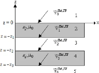
II. FORMULATION
We start the formulation from the equations that determine the reflected and transmitted
characteristics of a generalized periodic array [5].
(
)
2 2
s r s r
n xt x mn m yt y mn TE
mn
m n
j ( E E ) ( E E )
R
( )
β δ α δ
α β + − + = + ɶ ɶ (1)
(
)
2 2s t s t
n xb x mn m yb y mn TE
mn
m n
j ( E E ) ( E E )
T
( )
β δ α δ
α β + − + = + ɶ ɶ (2) where,
2 2 2
0
mn mn mn k
γ = α +β − (3)
1 0
0
mn
if m n
if m n
δ = = =
≠
(4)
The superscripts b and t in the scattered field (
E
ɶs) are related to fields in top and bottom of the structure, respectively. The fieldsE
r andE
t are the complementary reflected and transmitted fields. The scattered fields are obtained from:1 1 1 2 2 2
1 2
1 1 2 2
s
xxt ,b xyt ,b xxt ,b xyt ,b
xt ,b x x
s
yt ,b yxt ,b yyt ,b y yxt ,b yyt ,b y
Z Z Z Z
E J J
E Z Z J Z Z J
= +
ɶ ɶ ɶ ɶ
ɶ ɶ ɶ
ɶ ɶ ɶ ɶ ɶ ɶ ɶ (5)
where the superscripts 1 and 2 are related with the patch elements on dielectric layers 2 and 4, as we
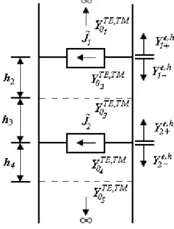
can see in Figure 1.
The next step is to find the components of the Dyadic Green’s function at interfaces 1-2 and 3-4.
These components are obtained as:
(
)
(
)
2 2
1 2 1 2
1 2 1 2 1 2 1 2
2 2
1 2 1 2 2 2
1 2 1 2 1 2 1 2
1
TM TE TE TM , ,
, , , ,
xx xy
, , TE TM TE TM
yx yy , , , ,
Z Z Z Z
Z Z
Z Z Z Z Z Z
β α αβ
α β αβ β α
+ − = + − +
ɶ ɶ ɶ ɶ
ɶ ɶ
Brazilian Microwave and Optoelectronics Society-SBMO received 29 Dec. 2011; for review 29 Dec. 2011; accepted 22 March 2012
Brazilian Society of Electromagnetism-SBMag © 2012 SBMO/SBMag ISSN 2179-1074 where,
1 2
1 2 1 2
1
TM ,TE
, e ,h e,h
, ,
Z
Y + Y −
=
+ ɶ
(7)
Fig. 1. Double screen FSS considered in analysis.
To obtain the admittances Y1 2e ,h, + and Y1 2e,h, − we will use the equivalent transmission line method [5]. The structure in Figure 1 will be represented by the circuit shown in Figure 2.
Fig. 2. Equivalent circuit to the structure considered in analysis.
For isotropic materials we define:
0
0
TE i i
Y j
γ ωµ
= (8)
0 0TMi ri
i
j
Y ωε ε
γ
= (9)
2 2 2
0 0
i mn mn ri
γ = α +β −ω µ ε ε (10)
where i = 1, 2, …, 5.
Brazilian Microwave and Optoelectronics Society-SBMO received 29 Dec. 2011; for review 29 Dec. 2011; accepted 22 March 2012
Brazilian Society of Electromagnetism-SBMag © 2012 SBMO/SBMag ISSN 2179-1074
( )
( )
0 0 0 L in LY Y coth h
Y Y
Y Y coth h γ γ +
=
+ (11)
where Y0 is the characteristic admittance of the medium and YL is the load admittance of the medium.
The admittances Y1e ,h+ and Y1e,h− are obtained turn off the current source Jɶ2, substituting it by an open circuit. In an analog way, the admittances Y2e ,h+ and Y2e,h− are obtained turn off the current source Jɶ1. Applying (11) in the circuit of Figure 2, we obtain the admittances Y1e ,h+ and Y1e,h− as:
1 01
e,h TM ,TE
Y+ =Y (12)
(
)
(
)
2 2 2
02
1 02
2 02 2 2
TM ,TE L e,h TM ,TE
TM ,TE L
Y Y coth h
Y Y
Y Y coth h
γ γ − + = + (13)
(
)
(
)
3 0 3
03 2 03
3 03 0 3
TM ,TE L TM ,TE
L TM ,TE L
Y Y coth h
Y Y
Y Y coth h
γ γ + = + (14)
(
)
(
)
4 4 4
04 3 04
4 04 4 4
TM ,TE L TM ,TE
L TM ,TE L
Y Y coth h
Y Y
Y Y coth h
γ γ + = + (15) 4 05 TM ,TE L
Y =Y (16)
Applying (11) for the current source 2 in the circuit of Figure 2, we obtain the admittance Y2e ,h+ as:
(
)
(
)
3 0 3
03
2 03
3 03 0 3
TM ,TE L e,h TM ,TE
TM ,TE L
Y Y coth h
Y Y
Y Y coth h
γ γ + + = + (17)
(
)
(
)
2 2 2
02 3 02
2 02 2 2
TM ,TE L TM ,TE
L TM ,TE L
Y Y coth h
Y Y
Y Y coth h
γ γ + = + (18) 2 01 TM ,TE L
Y =Y (19)
We obtain the admittance Y2e,h− as:
(
)
(
)
4 4 4
04
2 04
4 04 4 4
TM ,TE L e,h TM ,TE
TM ,TE L
Y Y coth h
Y Y
Y Y coth h
γ γ − + = + (20)
In (5), Jɶ1 and Jɶ2 are the current density components in the Fourier domain induced on the patches by the incident fields. These induced Fourier transformed current density components are expressed in terms of a set of basis function fi as:
i i i
J =∑C f
(21)
Considering the patches perfectly conducting we have:
0
s i
E +E = (22)
These unknown coefficients for Jɶ1 and Jɶ2 can be obtained by the incident fields at the planes z =
Brazilian Microwave and Optoelectronics Society-SBMO received 29 Dec. 2011; for review 29 Dec. 2011; accepted 22 March 2012
Brazilian Society of Electromagnetism-SBMag © 2012 SBMO/SBMag ISSN 2179-1074
Fig. 3. Incident potentials on conducting patches.
In according with [3] the incident potentials are given as:
0 0 0 0 0 0
j x j y z j x j y z
TE
o eα e β eγ Reα e β e−γ
Ψ = + (23)
[
]
0 0
1TE ejα x je β y C cosh(11 γ2 1z ) C senh(12 γ2 1z )
Ψ = − (24)
[
]
0 0
2 j x j y 21 0 2 22 0 2
TE e α e β C cosh(γ z ) C senh(γ z )
Ψ = − (25)
[
]
0 0
3 j x j y 31 4 3 32 4 3
TE eα e β C cosh(γ z ) C senh(γ z )
Ψ = − (26)
0 0 0
4 j x j y z
TE
Te α e β eγ
Ψ = (27)
To guarantee the continuity of the tangential fields at the dielectric interfaces, the incident fields are
given as [3]:
1
TE i i x
E
y −
∂Ψ = −
∂ (28)
1
TE i i y
E
x −
∂Ψ =
∂ (29)
2 1 0
1 TE
i i
x
H
jωµ x z −
∂ Ψ =
∂ ∂ (30)
2 1 0
1 TE
i i
y
H
jωµ y z −
∂ Ψ =
∂ ∂ (31)
So, to determine the unknown coefficients of the basis functions, we need the incident fields at
planes z = 0 and z = z2, using (28) to (31) and applying conditions of continuity in these planes we
obtain:
For z = 0:
0 0
1 0 0
0 0 2 3
1
2
inc
x j x j y inc
y
E
j e e
F E
α β β
γ
α
γ γ
−
=
+
Brazilian Microwave and Optoelectronics Society-SBMO received 29 Dec. 2011; for review 29 Dec. 2011; accepted 22 March 2012
Brazilian Society of Electromagnetism-SBMag © 2012 SBMO/SBMag ISSN 2179-1074 For z = −z2:
(
)
(
)
(
)
0 02 0 0 2 0
0 2 2 1 1 3
0 0 2 3
2
2
inc
x j x j y
inc y
E / sinh z
j coth z F A B F e e
F E
α β β
γ γ γ α γ γ − = − + + (33) where
2 1 1 3
1 2 1
F A C
F
D F B
− =
−
1 2 2 2
2 1 2
F A C
F
D F B
− =
−
(
)
(
)
4 0 4 3
1
0 4 4 3
coth z F
coth z
γ γ γ
γ γ γ
+ =
+
(
)
(
)
2(
)
(
)
1 0 1 2 1 0 1 2 1
0
A cosh γ z cosh γ z γ sinh γ z sinh γ z γ
= −
(
)
(
)
2(
)
(
)
1 0 1 2 1 0 1 2 1
0
B cosh γ z sinh γ z γ sinh γ z co sh γ z γ
= − +
(
)
(
)
2(
)
(
)
1 0 1 2 1 0 1 2 1
0
C sinh γ z cosh γ z γ cosh γ z sinh γ z γ
= −
(
)
(
)
2(
)
(
)
1 0 1 2 1 0 1 2 1
0
D sinh γ z sinh γ z γ cosh γ z cosh γ z γ
= − +
(
)
(
)
0(
)
(
)
2 4 2 0 2 4 2 0 2
4
A cosh γ z cosh γ z γ sinh γ z sinh γ z γ
= −
(
)
(
)
0(
)
(
)
2 4 2 0 2 4 2 0 2
4
B cosh γ z sinh γ z γ sinh γ z co sh γ z γ
= − +
(
)
(
)
0(
)
(
)
2 4 2 0 2 4 2 0 2
4
C sinh γ z cosh γ z γ cosh γ z sinh γ z γ
= −
(
)
(
)
0(
)
(
)
2 4 2 0 2 4 2 0 2
4
D sinh γ z sinh γ z γ cosh γ z cosh γ z γ
= − +
where z1=h2, z2=h2+h3, and z3=h2+h3+h4.
The unknown coefficients of the basis functions can be obtained numerically from (30) and (31) as:
2
1
mn mn
qi qi
inc
xx xy qx mn mn
ix j( x y )
inc q m n qi qi
qy mn mn
iy yx yy
Z Z J ( , )
E
e
J ( , )
E Z Z
α β α β α β ∞ ∞ + = =−∞ =−∞ − = ∑ ∑ ∑
ɶ ɶ ɶ
ɶ
ɶ ɶ (34)
where i = 1, 2.
The spectral variables, αmn and βmn, are defined as:
( )
( )
0 2
mn
m
k sen cos T
π
α = + θ φ (35)
( )
( )
0 2
mn
n
k sen sen T
π
Brazilian Microwave and Optoelectronics Society-SBMO received 29 Dec. 2011; for review 29 Dec. 2011; accepted 22 March 2012
Brazilian Society of Electromagnetism-SBMag © 2012 SBMO/SBMag ISSN 2179-1074 where T is the periodicity of the unit cells in x and y directions. The angles θ and φ are the incidence
angles and k0 is the wave number in free space.
As we can see in (1) and (2), the transmission and reflection coefficients have terms of reflected
and transmitted fields that are included when m = n = 0.
For the structure shown in Fig. 1, those reflected and transmitted fields are given as:
0
r x
Eɶ = −jβ R (37)
0
r y
Eɶ = jα R (38)
0 3
0 z
t x
Eɶ = −j Teβ −γ (39)
0 3
0 z
t y
Eɶ =j Teα −γ (40)
These coefficients are obtained during the procedure to determine the incident fields. They are
given as:
0 2 3 0 2 3
F R
F
γ γ
γ γ
− =
+ (41)
(
)
0(
4 3)
0 34 5
0 2 3
2 / sinh z z
T F F e
F
γ
γ γ
γ γ
= −
+
(42)
F3 was defined earlier and F4 and F5 are given as:
(
)
(
)
4 1 2 1 2 3 1 2 1 2 3 4 3
F = A A +B A F +C B +D B F coth γ z
5 1 2 1 2 3 1 2 1 2 3
F =A C +B C F +C D +D D F
To finish the formulation, we need to know that when the scattered fields are evaluated at a
distance h from the current source as depicted in Figure we need to modify (7). To transfer the
impedances ZTM,TE to a distance h we need to multiply (7) by the factor:
( )
( )
0 0
transfer
L
Y Y
Y cos γh Y sin γh
=
+ (43)
Therefore,
1 2
1 2 1 2
1
TM ,TE
transfer
, e,h e ,h
, ,
Z Y
Y + Y −
=
+ ɶ
(44)
If the scattered fields are evaluated two layers from the source we need to multiply (44) by (43)
with YL, Y0, γ and h replaced by the new ones.
To obtain the scattered fields at the top of the structure, we need to transfer
Z
ɶ
2TM ,TE as:1 2
2
2 2
1
TM ,TE
transfer transfer e ,h e ,h
Z Y Y
Y + Y −
= + ɶ
(45)
Brazilian Microwave and Optoelectronics Society-SBMO received 29 Dec. 2011; for review 29 Dec. 2011; accepted 22 March 2012
Brazilian Society of Electromagnetism-SBMag © 2012 SBMO/SBMag ISSN 2179-1074
(
)
(
)
1 03
03 0 3 3 0 3
transfer
L
Y Y
Y cos γ h Y sin γ h
=
+ (46)
(
)
(
)
2 02
02 2 2 2 2 2
transfer
L
Y Y
Y cos γ h Y sin γ h
=
+ (47)
where Y0TM ,TEi , YL2 and YL3 were defined in (8), (9), (19) and (20), respectively.
To obtain the scattered fields at the top of the structure, we need to transfer the impedances as:
1 2 3
1
1 1
1
TM ,TE
transfer transfer transfer e ,h e ,h
Z Y Y Y
Y+ Y−
= + ɶ
(48)
where,
(
)
(
)
1 02
02 2 2 2 2 2
transfer
L
Y Y
Y cos γ h Y sin γ h
=
+ (48)
(
)
(
)
2 03
03 0 3 3 0 3
transfer
L
Y Y
Y cos γ h Y sin γ h
=
+ (48)
(
)
(
)
3 04
04 4 4 4 4 4
transfer
L
Y Y
Y cos γ h Y sin γ h
=
+ (48)
The admittances YL2, YL3 and YL4 were defined in (13), (14) and (15), respectively.
For the current source 2 we have:
1 2
2 2
1
TM ,TE
transfer e ,h e ,h
Z Y
Y + Y −
= + ɶ
(49)
where Ytransfer1 is the same of (48).
III. RESULTS
To validate our analysis, we compare our simulated results with measurements and simulations
presented in [15] and [16]. The used element in unit cells was the rectangular patch. The periodicity
was equal to 22 mm. In structure 1 the dimensions of the patch were w = 7 mm and L = 10 mm. In
structure 2 the dimensions of the patch were w = 8 mm and L = 8 mm. The structures were built on a
dielectric with εr = 3.9 and a thickness equal to 1.5 mm. in our simulations we used 6 basis functions
and the number of spectral terms ranging from 200 to 10,000.
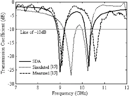
Figure 4 shows a comparison between numerical and measured results for a cascading structure.
The air gap between structures was 1.5 mm. The structures are cascaded using Teflon spacers and
screws to obtain the air gap. For this air gap between structures we can see that appear two resonances
for our simulated results and those presented in [15]. Measured results present resonance frequencies
equal to 9.07 GHz and 10.59 GHz, our simulated results present resonance frequencies equal to 8.99
GHz and 10.29 GHz, and simulated results presented in [15] present resonance frequencies equal to
Brazilian Microwave and Optoelectronics Society-SBMO received 29 Dec. 2011; for review 29 Dec. 2011; accepted 22 March 2012
Brazilian Society of Electromagnetism-SBMag © 2012 SBMO/SBMag ISSN 2179-1074 MHz, our simulated results were equal to 329 MHz and 329 MHz, and simulated results presented in
[15] were equal to 517 MHz and 360 MHz. So, we obtained a better agreement with measured results
for the spectral domain analysis (SDA) presented in this paper.
Fig. 4. Structure response for an air gap of 1.5 mm.
Figure 5 shows a comparison between numerical and measured results for a cascading structure.
The air gap between structures was 3.0 mm. For this space between structures we can see that again
appear two resonances for our simulated results and those presented in [15]. Measured results present
resonance frequencies equal to 9.30 GHz and 10.48 GHz, our simulated results present resonance
frequencies equal to 9.27 GHz and 10.89 GHz, and simulated results presented in [15] present
resonance frequencies equal to 9.49 GHz and 10.25 GHz. The bandwidths for measured results were
equal to 361 MHz and 596 MHz, our simulated results were equal to 361 MHz and 423 MHz, and
simulated results presented in [15] were equal to 611 MHz and 267 MHz. For the first resonance our
results obtained a better agreement with measured results. This also occurs for the bandwidths. The
worst difference between our results and those measured in [15] for the second resonance frequency is
probably due to the number of basis functions used.
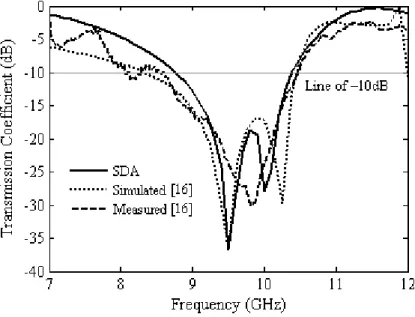
Figure 6 shows a comparison between numerical and measured results for a cascading structure.
The air gap between structures was 6.0 mm. The measured results were presented in [16]. For this air
gap we can see that appear only one resonance. Measured results present a resonance frequency equal
to 9.72 GHz, our simulated results present resonance frequency equal to 9.70 GHz, and simulated
results presented in [16] present resonance frequency equal to 9.50 GHz. The bandwidth for measured
results was equal to 1.83 GHz, for our simulated results it was equal to 1.24 GHz, and for simulated
results presented in [16] it was equal to 1.91 GHz. We obtain a better result for resonance prediction
Brazilian Microwave and Optoelectronics Society-SBMO received 29 Dec. 2011; for review 29 Dec. 2011; accepted 22 March 2012
Brazilian Society of Electromagnetism-SBMag © 2012 SBMO/SBMag ISSN 2179-1074
Fig. 5. Structure response for an air gap of 3.0 mm.
Fig. 6. Structure response for an air gap of 6.0 mm.
Figure 7 shows a comparison between numerical and measured results for a cascading structure.
The air gap between structures was 8.0 mm. The measured results were presented in [16]. For this air
gap we can see that appear only one resonance. Measured results present a resonance frequency equal
to 9.82 GHz, both simulated results presented in this paper and those presented in [16] obtain a
resonance frequency equal to 9.50 GHz. The bandwidth for measured results was equal to 1.83 GHz,
for our simulated results it was equal to 1.24 GHz, and for simulated results presented in [16] it was
equal to 1.91 GHz. For this air gap the results presented in [16] obtain a better agreement with
measured results.
Figure 8 shows a comparison between numerical and measured results for a cascading structure.
The air gap between structures was 10.0 mm. The measured results were presented in [15]. Measured
Brazilian Microwave and Optoelectronics Society-SBMO received 29 Dec. 2011; for review 29 Dec. 2011; accepted 22 March 2012
Brazilian Society of Electromagnetism-SBMag © 2012 SBMO/SBMag ISSN 2179-1074 presented in [15] obtain resonance
frequencies
equal to9.50GHz and 10.25GHz
. Our resultspresented two resonances frequencies equal to 9.39 GHz and 10.21 GHz. For this air gap our results
obtain a better agreement with measured results.
Fig. 7. Structure response for an air gap of 8.0 mm.
Fig. 8. Structure response for an air gap of 10.0 mm.
Comparing the analysis performed in this work with the one developed in [15] some
observations can be made. For small gaps, the analysis performed in this paper provides more
accurate results. In fact, as the air gap increases the results did not differ so much. With
respect to computational effort, the approximate analysis of [15] presents a high
computational effort to get the results of single FSS. After this, the approximated cascading
Brazilian Microwave and Optoelectronics Society-SBMO received 29 Dec. 2011; for review 29 Dec. 2011; accepted 22 March 2012
Brazilian Society of Electromagnetism-SBMag © 2012 SBMO/SBMag ISSN 2179-1074
presents a high computational effort, for all structures analyzed, and is compatible with
commercial computer programs as Ansoft Designer
TMand CST Studio, for example.
IV. CONCLUSIONS
The entire formulation to get the scattering of electromagnetic waves from a double screen FSS
with conducting patch elements on isotropic materials was presented, in the spectral domain, for the
determination of the reflection and transmission coefficients. The spectral domain immitance
approach and the method of moments were used to get the characteristics of the FSS structures with
patches. Numerical results obtained in this work were compared with simulations and measurements
presented by another authors. For low air gap values, our results obtained a much better agreement
with measurements when compared with the simulations presented in [15]. The accurate of the results
is strongly dependent of the number of basis functions used in the analysis. A convergence study must
be done to investigate this better.
REFERENCES
[1] B. A. Munk, “Frequency Selective Surfaces – Theory and Design”, Jonh Wiley & Sons, New York, USA, 2000.
[2] T. K. Wu and S. W. Lee, “Multiband Frequency Selective Surface with Multiring Patch Elements”, IEEE Transactions on Antennas and Propagation, Vol. 42, No. 11, pp. 1484 – 1490, 1994.
[3] S. B. Savia and E. A. Parker, “Superdense FSS with Wide Reflection Band and Rapid Rolloff”, Electronic Letters, Vol. 38, No. 25, pp. 1688, 2002.
[4] G. Q. Luo et al., “Design and Experimental Verification of Compact Frequency-Selective Surface With Quasi-Elliptic Bandpass Response”, IEEE Transactions on Microwave Theory and Techniques, Vol. 55, No. 12, pp. 2481 – 2487, 2007.
[5] T. K. Wu, “Frequency selective surface and grid array”, Jonh Wiley & Sons, New York, USA, 1995.
[6] T. L. Silva and A. L. P. S. Campos, “Formulation of Double Screen FSS Analysis Using Fullwave Method”, International Microwave and Optoelectronics Conference, pp. 512 – 516, 2011.
[7] R. Dubrovka, J. Vazquez, C. Parini e D. Moore, “Multi-frequency and multi-layer frequency selective surface analysis using modal decomposition equivalent circuit method”, IET Microwave Antennas & Propagation, Vol. 30, No 3, pp. 492 – 500, 2009.
[8] S. W. Lee, G. Zarrillo e C. L. Law, “Simple formulas for transmission through periodic metal grids or plates”, IEEE Transactions on Antennas and Propagation. 30 (5), 904 – 909 (1982).
[9] T. Cwik e R. Mittra, “The cascade connection of planar periodic surfaces and lossy dielectric layers to form an arbitrary periodic screen”, IEEE Transactions on Antennas and Propagation, AP-35 (12), 1397 – 1405 (1987).
[10] J. D. Vacchione e R. Mittra, “A generalized scattering matrix analysis for cascading FSS of different periodicities”, International IEEE Antennas and Propagation Symposium Digest, Dallas, TX, 1, 92 – 95, 1990.
[11] J.-F. Ma e R. Mittra, “Analysis of multiple FSS screens of unequal periodicity using an efficient cascading technique”, IEEE Trans. Antennas Propag. 53 (4), 1401 – 1414 (2005).
[12] R. H. C. Manioba, A. G. d'Assunção and A. L. P. S. Campos, “Improving Stop-Band Properties of Frequency Selective Surfaces with Koch Fractal Elements”, International Workshop on Antenna Technology, pp. 1 – 4, 2010.
[13] A. C. C. Lima and E. A. Parker, “Fabry-Perot Approach to the Design of Double Layer FSS”, IEE Proceedings, pp. 157 – 162, 1996. [14] R. D. Nair, A. Neelam and R. M. Jha, “EM Performance Analysis of Double Square Loop FSS Embedded C-sandwich Radome”,
Applied Electromagnetic Conference, pp. 1 – 3, 2009.
[15] A. L. P. S. Campos, R. H. C. Maniçoba_, L. M. Araújo_, and A. G. d’Assunção, “Analysis of Simple FSS Cascading With Dual Band Response”, IEEE Transactions on Magnetics, Vol. 46, No. 8, pp. 3345 – 3348, 2010.