Pulsed laser rystallization of SiGe alloys on GaAs
F. Dondeo, 1
P. V. Santos, 2
M.Ramsteiner, 2
D. Comedi, 1
M. A.A. Pudenzi, 1
, and I. Chambouleyron 1
1
InstitutodeFsiaGlebWataghin,UniversidadeEstadual deCampinas, 13081-970Campinas,SP,Brazil
2
Paul-Drude-Institut f urFestkorperelektronik, Hausvogteiplatz5{7, 10117Berlin,Germany
Reeivedon23April,2001
We have investigated the rystallization of amorphous SiGe lms deposited onrystalline GaAs
(001) substrates using ns laser pulses. Analysisof the lm struture usingRaman spetrosopy
indiatestheformationofheteroepitaxialSixGe1 x/GaAsstruturesforSiompositionsuptox =
25%. Higherompositionslead topolyrystallinelms. Thisisattributedtotheinreasedlattie
mismathbetweenSixGe1
x
andGaAsastheSifrationinthealloyinreases.
I Introdution
Pulsedlaserrystallization(LC)[1℄isastandard
teh-nique for the fabriation of large area polyrystalline
lms from theamorphous (a-) phase. This tehnique
analso beused to produe high quality epitaxial Ge
layerswithabruptinterfaesonGaAs (001)substrates
[2℄. Sine Ge and GaAs are well lattie-mathed, an
interesting question is how the epitaxial LC proeeds
when Si is introdued in aontrolled wayinto the Ge
matrix, so as to form Si
1 x Ge
x
alloys with a lattie
onstant dierent from that of the substrate. In this
ontribution,weaddressthisquestionbyinvestigating
theLC of a-Si
x Ge
1 x
alloysdeposited onGaAs (001)
substrates. Raman sattering studies of the LC lms
giveevidenefortheepitaxialrystallizationof
100-nm-thik Si
x Ge
1 x
alloys withompositions x upto 25%.
Higherompositionsleadtopolyrystallinelms. This
behaviorisattributedtotheinreasedlattiemismath
with the substrate, when the silion onentration in
the alloy inreases. Sine the epitaxial rystallization
requiresthemeltingoftheamorphouslmbythelaser
pulse, aseond important issueregarding the
rystal-lizationofSi
x Ge
1 x
alloysonGaAsistheintermixing
at the interfae with the substrate. The intermixing
was investigated using seondaryion mass
spetrome-try(SIMS).
II Experimental
The a-Si
x Ge
1 x
samples were grown by
ion-beam-assisted sputteringon GaAs (001) substrates. Before
lm deposition, the substrates were heated to 350 Æ
C
andbombardedbya30eVhydrogenionbeamfor1min
removal wasmonitored in-situ using x-ray
photoele-tron spetrosopy. 100-nm-thik a-Si and a-Ge lms
were thendeposited from Si and Ge targets(99.999%
pure) using 1000 eVKr +
ionsfrom aKaufmanngun.
a-Si
0:1 Ge
0:9
lmsofthesamethiknessweregrown
us-ing a Ge target overed with a piee of Si. In order
to obtainlaserrystallizedSi
x Ge
1 x
alloyswithother
ompositions x (x = 0.25, 0.50, and 0.75), a-Si/a-Ge
multilayerswithindividualSi andGelayerthiknesses
below 25 nmwere deposited. Eah multilayersample
onsists of 6 layers adding up to a total thikness of
100nm. Aswillbedemonstratedbelow,thelayers
om-pletelyintermixduringthelaserrystallizationproess,
leadingto the formationof ahomogeneousrystalline
(-)SiGealloywiththeompositiondeterminedbythe
relativethiknessesoftheoriginala-Geanda-Silayers.
The samples were rystallized with single pulses
(pulsewidthofapprox. 7ns)fromafrequeny-doubled
Nd:Yaglaser(=532nm). AGaussian-likelaserbeam
prolewithadiameter ofapprox. 4mmwasobtained
byusingavauumspatiallter. Thelaserpulse
uen-ieswereestimatedfromthemeasuredpulseenergyby
assumingaGaussianproleforthedistributionoflight
intensity on the irradiated area. The rystallization
proess was monitored in-situ by reording the
tran-sientreetivityofawdiodelaserbeam(=675nm)
during theLCproess. Theinreaseinthereetivity
indiates thatthea-SiGe alloysmeltduring laser
irra-diation[3℄.
Raman spetrosopy was employed to study the
strutural properties of the samples. The
measure-ments were performed at room temperature in the
baksattering geometry using the z(x; y)z, z(y; y)z,
z(x 0
; y 0
)z, and z(y 0
; y 0
)z sattering ongurations,
wherex;y;z;z;x 0
andy 0
denote,respetively,the[100℄,
retions of the (001) GaAs substrates. Note that
de-formation potential Ramansattering by longitudinal
optial(LO)phononsisallowedbyseletionrulesonly
for theongurationsz(x; y)z andz(y 0
; y 0
)z [4℄. The
redlines(
L
=676:4or647.1nm)ofaKr +
-laserwere
used forexitation.
250
300
350
400
450
500
λ
L
= 676.4 nm
Si
0.25
Ge
0.75
LO-GaAs
Ge-Ge
Ge-Si
Si-Si
z(y',y')z
z(x',y')z
In
te
n
s
ity
(a
rb
. u
n
its
)
Raman Shift (cm
-1
)
Figure 1. Raman spetra of a LC -Si
0:25 Ge
0:75 alloy
reorded inthe z(y 0
; y 0
)z (thik line, upperurve)and in
the z(x 0
; y 0
)z (thin line,lowerurve)sattering
ongura-tions. Thelaseruenywasapprox. 500mJ/m 2
.
III Results and Disussion
The Raman spetra of as-grown a-SiGe multilayers
showbroadRamanlinesentered around270and470
m 1
,whihareattributed totheGe-Geand Si-Si
vi-brationsofthea-Geanda-Silayers,respetively. After
LC, these lines narrowand shift somewhat in energy.
ARamanspetrumofaLC-Si
0:25 Ge
0:75
alloywithan
averageompositionx=25%reordedinthez(y 0
; y 0
)z
ongurationis shown by thesolidline in Fig.1. The
three mainpeaksfoundat290,400and470m 1
or-respond,respetively,toGe-Ge,Ge-SiandSi-Si
vibra-tionsofa-Si
0:25 Ge
0:75
alloy[5℄. TheGe-Siline,whih
onlyappearsafterLC,evidenestheintermixingofthe
SiandGelayersduringlaserirradiation. Thesharpline
at292m 1
(losetotheGe-Gevibration)orresponds
to satteringbyLOphononsin theGaAssubstrate.
Thespetrumreorded in the forbiddenz(x 0
; y 0
)z
ongurationin Fig. 1(thin line)showsastrongly
re-duedsatteringintensity. Thisredutionisattributed
to theepitaxialorientationoftheSi
0:25 Ge
0:75
lm
rel-ativeto the GaAs substrate. Similarresultswere also
obtainedforalloyswithx =10%. Onlypolyrystalline
regionswereobservedforx>25%,thusindiatingthat
thelargemismath preventstheformationof epitaxial
lms.
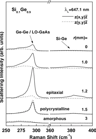
TheRamanspetrumandthusthestrutureofthe
LClayersdependssensitivelyonthelaserpulseueny.
Thisresultisillustratedin Fig. 2,whihdisplaysa
se-250
275
300
360
380
400
λ
L
=647.1 nm
r(mm)=
Si-Ge
epitaxial
polycrystalline
Ge-Ge / LO-GaAs
amorphous
Si
0.1
Ge
0.9
3
1.5
1.2
1.0
0
Scattering Intensity (arb. units)
Raman Shift (cm
-1
)
z(x,y)z
z(y,y)z
Figure2. RamanspetraofaLC-Si
0:1 Ge
0:9
alloyreorded
atdierentradialdistanesrfromtheenteroftheLCspot.
Theueniesforx=0,1,1.2,1.5,and3mmareestimated
tobe2000,1250, 1000,650,and0mJ/m 2
.
distanesr fromtheenterofthespotproduedbyLC
onamultilayerwithx=0.10. Thelaserpulse ueny
dereases with r following theGaussian-likeprole of
the laser beam. Forlarge distanes (r = 3 mm), the
pulse energy is insuÆient to indue the phase
tran-sition, so that the material remains amorphous. For
r = 1.5 mm, omparable intensities are measuredin
the z(x; y)z and z(y; y)z geometries, thus indiating
theformationofapolyrystalline-Si
0:1 Ge
0:9
alloy. For
r <1.2mm,theratiobetweenthesatteringintensities
intheallowedandforbiddensatteringgeometries
be-omesverylarge. Weattribute this large ratioto the
formationof anepitaxiallmwith thesame
rystallo-graphiorientationasthesubstrate.
The laser ueny of 1000 mJ/m 2
estimated for
r=1.2 isapproximatelythesameasthat required to
obtainhighqualityLC-GelmsonGaAs. Althoughthe
materialstillrystallizesepitaxiallyforr <1.2mm,the
peakintensityoftheRamanlinesatapprox. 290m 1
reordedin theallowedsattering onguration(thik
0
5
10
15
10
1
10
2
10
3
10
4
10
5
10
6
10
7
10
1
10
2
10
3
10
4
10
5
10
6
10
7
(b)
Ge
Si
Ga
counts/s
sputtering time (min)
(a)
counts/s
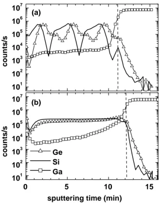
Figure3. ConentrationsofGe,Si,andGaasafuntionof
SIMSsputteringtimeforana-Si/a-Gemultilayer(a)before
and(b)afterLC. Theompositionofthe-Si
x Ge
1 x alloy
isx=0:25. Theoriginalpositionof theinterfaewiththe
substrateisindiatedbythevertialdashedline.
the high temperatures indued in the Si
1 x Ge
x layer
under high laser uenies, whih leads to strong
ma-terialintermixingattheGaAs/Si
1 x Ge
x
interfaeand,
eventually,toapartialmeltingoftheunderlyingGaAs.
WhentheSi
1 x Ge
x
alloyrystallizes,itsabsorption
o-eÆient dereases, and it beomes almost transparent
totheinident(andsattered)light. Asaresult,a
sub-stantial fration of the Raman signal deteted in LC
lmsoriginatesfromthemateriallosetotheinterfae
with the substrate. The broadened Raman line
en-tered at280m 1
is attributed tothesattering from
oupled LO-phonon-plasmonmodes in theintermixed
p-typeGaAs:Gelayer[6, 7℄.
Thestrongintermixingfor high pulseuenies
be-omesevidentin theSIMSprolesdisplayedinFig.3,
whihwerereordedonana-Si/a-Gemultilayerbefore
[Fig.3(a)℄andafter LC [Fig.3(b)℄. TheSIMS
experi-beam. The dashed vertial lines indiate the original
positionoftheSi
0:25 Ge
0:75
/GaAsinterfae,loated
ap-prox. 100nmbelowthesurfae. Themodulationofthe
Ge andSi onentrationsin theas-grownmultilayeris
evidentinFig.3(a). Thismodulationdisappearsasthe
individualSiandGelayersompletelyintermixduring
LC, giving rise to a homogeneous -Si
0:25 Ge
0:75 lm
[Fig. 3(b)℄. The proles also show a strong
interdif-fusion of Ga into the -Si
0:25 Ge
0:75
lm and a muh
less pronouned diusion of Ge and Si into the
sub-strate. Arsenidiusion(notshown)wasalsoobserved
in SIMSproles measured with aesium primary ion
beam.
IV Conlusions
Inonlusion,wehavestudiedthestrutureofLCSiGe
alloysgrownon(001)GaAssubstrates. Epitaxiallms
with a thikness of 100 nm were obtained for Si
on-entrations up to 25%. Higher Si onentrations lead
to polyrystallinelms.
Aknowledgments
The investigation are partially supported by a
DAAD(Germany)- CAPES(Brazil)international
o-operationprogram.
Referenes
[1℄ J.M.PoateandJ.W.Mayer,LaserAnnealingof
Semi-ondutors (AademiPress,New York,1982).
[2℄ J.E.Greene,K.C.Cadien,D.Lubben,G.A.Hawkins,
G.Erikson,andJ.R.Clarke,Appl.Phys.Lett.39,232
(1981).
[3℄ G. Aihmayr, D. Toet, M. Mulato, P. V. Santos, A.
Spangenberg, S. Christiansen, M. Albreht, and H. P.
Strunk,J.Appl.Phys.85,1040(1999).
[4℄ M.Cardona,LightSattering inSolidsII,(Ed.M.
Car-dona and G.Guntherodt, Springer, Berlin, 1982), pp.
153.
[5℄ M. A.Renui,J.B.Renui,and M.Cardona, Light
Sattering in Solids, (Ed. M. Balkanski, Flammarion,
Paris,1971),pp.326-329.
[6℄ A.Mlayah, R.Carles, andA.Leyuras, J.Appl.Phys.
71,422(1992).
[7℄ D.OlegoandM.Cardona,SolidStateCommun.32,375