Interfaial Layers and Impurity Segregation
in InP=In
0:53 Ga
0:47
As Superlatties
L.K. Hanamoto a
, A.B. Henriques a
, C. V.-B. Tribuzy b
, P. L. Souza b
,
B. Yavih b
, and E. Abramof
a
Instituto deFsia,Universidadede S~aoPaulo,CaixaPostal 66318,05315-970, S~aoPaulo,Brazil;
b
CentrodeEstudos emTeleomunia~oes,PontifiaUniversidade Catolia,
RuaMarqu^esdeS~aoViente, 225,22453-900, Rio deJaneiro,Brazil;
LAS-INPE, Av. dosAstronautas,1758-Jd.Granja, 12227-010,S~aoJosedosCampos,S.P.,Brazil.
Reeivedon23April,2001
The interfaes in InP=In
0:53 Ga
0:47
As superlatties modulation doped with Si were investigated
usingmagneto-transport,apaitane-voltage,andhighresolutionX-raydirationmeasurements.
Results indiatethatathikinterfaial layerisformedwhenInPis grownontopofInxGa1 xAs,
andthatSiatomsthatfallintheinterfaiallayerhaveahighprobabilityofnotformingashallow
donorenter. Usingasimpletheoretialmodelthewidthoftheinterfaiallayerwhihwasestimated
tobe71monolayers.
I Introdution
The ability to produe abrupt interfaes between
epitaxial layers is important in manufaturing
mod-ernoptoeletronidevies,beausegradedinterfaesan
disrupt the optial spetra [1℄ and redue arrier
mo-bility [2℄, hindering devie appliations [3℄. For this
reason,many eortshavebeenspent to attainabrupt
interfaesinheterostrutures.
To improve interfaes, a ommonly used
proe-dure onsists in an interruption of the growth
pro-essbetweenthegrowthoftwodierentlayers[4℄-[10℄.
ForInP/In
0:53 Ga
0:47
Assystemsgrownbymetalorgani
vapour phase epitaxy, during growth interruptionthe
growth hamber is kept under a ow of the group V
element(P,As)of thelayerto begrownsubsequently.
For interruption times of 1s, the interfae between
In
0:53 Ga
0:47
As grown on InP (the so-alled upper
in-terfae) is abrupt [5, 6℄. However, an adequate
pro-edure to obtain an abrupt interfae for InP grown
on In
0:53 Ga
0:47
As (the so-alled lower interfae) has
not been reported yet. The lowerinterfae is always
graded, and ontains an interfaial layer of hemial
omposition InAs
x P
1 x
. Theinterfaiallayeroupies
the spae whih in an ideal struture would be
ou-pied by pure InP and the thikness and the hemial
ompositionoftheinterfaiallayerareverysensitiveto
the growth onditions [5℄-[10℄. To establish the ideal
growthonditions,reliableexperimentalproeduresto
haraterizetheinterfaesareneeded. However,thisis
a diÆulttask, due to the limitations inherent to the
resolution X-ray diration (HRXRD) and SIMS [7℄.
FromHRXRDmeasurementsonshortperiod
superlat-ties,whentheX-rayspetrashowfewsatellitepeaks,
thethiknessandthestrainoftheinterfaiallayer
an-not be established independently, onlythe produt of
thesequantitiesanbedetermined[8℄. SIMS
measure-mentsarelimitedin resolutionduetoraterurvature
and the knok-on eet [11℄, and annot be used to
deduethethiknessofanindividuallayerwithan
a-uraygreaterthan15
A[10℄.
Inthis workwepresentastudyoftheinterfaesin
InP=In
0:53 Ga
0:47
As superlatties using a ombination
of HRXRD, apaitane-voltage (C-V) and
magneto-transport measurements. The analysis of the entirety
oftheresultsobtainedallowsustoestimatethe
thik-ness of the interfaial layer at the lower interfae to
be 6-8 monolayers(ML) (1 monolayer 3
A) in our
samples.
II Experimental proedure
InP=In
0:53 Ga
0:47
Assuperlattiesmodulationdoped
with Si in the middle of InP barriers were grown by
low pressure metalorgani vapor phase epitaxy
(LP-MOVPE).Growthwasinterruptedattheinterfaesfor
1s, during this timeintervalthegrowthhamberwas
keptundertheowofgroupVelementofthelayertobe
deposited subsequently, in aordaneto the
presrip-tion whih yielded thebest interfaes reported sofar.
nessoftheIn
0:53 Ga
0:47
As layers(50
A),butdieredin
thethiknessoftheInPlayersandin thedopinglevel.
Furtherdetailsontheexperimentaltehniquesusedan
befoundinRef.[13℄.
III Results and disussion
Inordertodeterminetheharateristiwidthofthe
layersdopedwithSiinoursamples,theC-Vspetrum
oftheontrolsample311wasmeasured,whihonsists
ofathikInPlayerontainingasinglerystallineplane
dopedwithSi (delta-dopedlayer). TheC-Vspetrum
wasreproduedtheoretiallyfollowingthepresription
desribedinRef. [14℄. Fig. (1)showstheexperimental
and theoretialC-Vspetra,whih determinethat the
Siatomsaredistributedinalayerwhoseharateristi
width is w =18
A (6 ML). Thenon-zero thiknessof
the Si layer is a onsequene of impurity segregation
during thegrowthproess,whereasdiusionis
negligi-ble[15℄. Thethiknessw=6MLshowsthatinour
sam-plesSi segregationismuhlesseetivethanfoundby
Skuras etal [15℄in samplesgrownbyMBE,whereby
the harateristiwidth of the doped layerwas found
to be45ML.
Figure1. C-Vspetrumofsample311. Thesquaresarethe
experimentaldataandthesolidlineisthetheoretialurve.
Thesuperlattieperiodofthesampleswasobtained
from their HRXRD spetra; the thikness of the InP
layerswas obtainedbysubtrating thenominal
thik-nessoftheIn
0:53 Ga
0:47
Asfromthesuperlattieperiod.
The density of free arriers was dedued from a two
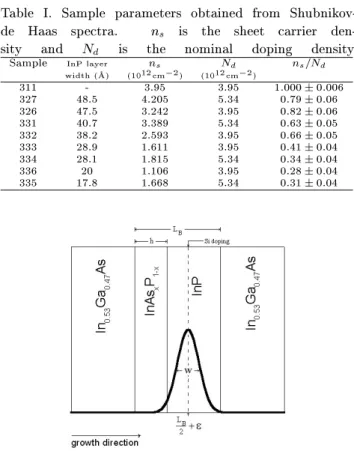
arrierttothemagnetoresistanedata. Table1
sum-marizes the results. The valueof N
d
givenin Table1
orrespondstothenominalvalueofthearealdensityof
ativeSiatomsin eahInPbarrier,whihwasderived
fromtheShubnikov-deHaasspetraofdelta-doped
lay-ers grown under the same onditions. Table 1 shows
thatthedensityoffreearriersdereaseswiththe
thik-nessoftheInPlayers. Fornarrowbarriers,the
proba-bilitythatagivenSiatomfallsintoaninterfaiallayer
is greaterthanforthikerones. Thustheobserved
de-number of Si atoms that areloatedin the interfaial
layers. ThissuggeststhattheSiatomsattheinterfaes
arenoteletrially ative. Thepossibility thattheseSi
atoms form shallowomplexes is also exluded, given
thatthemeasureddensityoffreearriersdoesnot
dis-play ativated behavior in the 2-300 K temperature
range. A possible explanation is that some of the Si
atoms loatedwithin the interfaial layers form
nega-tivelyharged DX enters [16,17℄. Thedisorderand
mehanialstrain, whih are present at the interfaes
[9℄favortheformationofDXenters[17℄.
Table I. Sample parameters obtained from
Shubnikov-de Haas spetra. ns is the sheet arrier
den-sity and Nd is the nominal doping density.
Sample InPlayer ns Nd ns=Nd
width(
A) (10 12
m 2
) (10 12
m 2
)
311 - 3.95 3.95 1:0000:006
327 48.5 4.205 5.34 0:790:06
326 47.5 3.242 3.95 0:820:06
331 40.7 3.389 5.34 0:630:05
332 38.2 2.593 3.95 0:660:05
333 28.9 1.611 3.95 0:410:04
334 28.1 1.815 5.34 0:340:04
336 20 1.106 3.95 0:280:04
335 17.8 1.668 5.34 0:310:04
Figure2. A Siplanar doped InP=In0:53Ga0:47As
superlat-tie with an interfae layer of InAsxP1
x
(with width h),
betweenInPgrownonIn0:53Ga0:47As.
Tomodeltheoretiallytheredutionoffreearriers
when the thikness of InP barriers dereases, we will
assume that the upper interfae is ideal, whereas the
lowerone isgraded, with aninterfaial layerof
thik-ness h. The Si atoms are supposed to be distributed
statistially along the growth axis in aordane with
aGaussianoffull widthofhalf maximumequaltothe
harateristiwidthofthedopinglayer,i.e. w=6ML.
Due to the segregationeet, theenter of the
Gaus-sianisallowedtobedisplaedfromtheenteroftheInP
barriers,by thesegregationlength, ". Fig. (2) shows
shematially theepitaxial layers,the interfaial layer
andthestatistialdistributionofSiatoms. Weassume
that agiven Si atom hasaprobability pof forming a
in-theamountoffreearriers,asafuntion ofthebarrier
width,L
B
,isgivenby:
n
s
N
d =
1 p
erf
p
4ln2
w
LB
2
+(h LB)(LB h) "
erf p
4ln2
w
LB
2 "
(1)
where N
d
isthe arealdensityof Si atoms introdued
into eah of the InPbarriers, (x)=1 if x >0; and
(x)=0ifx<0,anderf(x)istheerrorfuntion:
erf(x)= 2
p
Z
x
0 e
u 2
du (2)
Fig. (3)showstheexperimental dataand thebest
theoretialtusingEq. (1),wherebythetting
param-etersareh,p,and". Forthedottedurve,segregation
was notallowedfor and " was xed at zero; this
pro-dues a lower bound estimate of the thikness of the
interfaial layer, whih is found to be h =6 ML, for
p=0:51. Forthe ontinuousurve," wasfreeto
ad-just itself,resultingin "=1ML, aninterfaiallayerof
71ML,andp=0:480:05. Thesmallvalueof"
ob-tained is supportiveof our earlier onlusionthat the
segregation eet is pratially absent in the samples
usedinthis work.
Figure 3. Experimental data and modelurves given by
Equation1,with"=0(dotedurve)and"=1ML(solid
urve).
UsingtheanalysisofHRXRDmeasurements,Jiang
et. al. [9℄ estimated that for a In
0:53 Ga
0:47
As/ InP
(112
A/36
A)superlattie,thelowerinterfaelayerisof
InAs
0:28 P
0:72
omposition,with athiknessof12 ML.
Thesamplestudied wasgrownunderverysimilar
on-ditionstotheonesusedbyus. Jiang[9℄suggestedthat
thethiknessoftheinterfaiallayerinreaseswiththe
amount of residual As in the growth hamber. The
amountofAsinthegrowthhamberinreaseswiththe
thiknessoftheIn
0:53 Ga
0:47
Aslayerjustgrown. From
the data reported by Jiang and o-workers[9℄, it an
the order of 5.3 ML forevery50
A of In
0:53 Ga
0:47 As.
This result is quite similar to the one obtainedby us
foroursamples,allofwhihhadthesamethiknessof
50
Ain theIn
0:53 Ga
0:47
Aslayers,andwhoseinterfaial
layerweestimatedto beofthikness7ML.
Furthersupporttotheonlusionthatoursamples
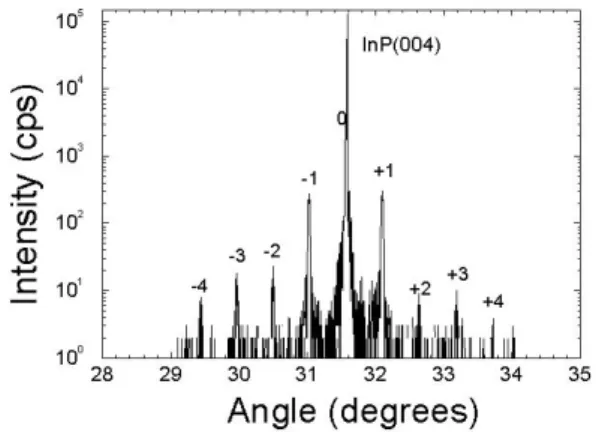
ontainathiklowerinterfaeanbeseeninFig. (4),
whihdepitsatypialHRXRDspetrumforour
sam-ples. TheHRXRDspetrumexhibitssatellitepeaksof
order+2,+3,and+4muhlessintensethanthepeaks
of order -2,-3, and -4,respetively, whih is aditional
evideneofthepreseneofaninterfaiallayer[9℄.
IV Conlusions
It was found that the density of free arriers in
modulation-dopedInP/In
0:53 Ga
0:47
Assuperlatties
de-reases veryrapidly when thewidth of the InPlayers
in the struture dereases. The redutionin the free
arrier density orrelates with the number of doping
atoms whih fall in the interfaial layer formed when
InP isgrown ontop ofIn
x Ga
1 x
As. Usingthe
trans-portdata andassumingthe spatialdistribution of the
Si atoms to be as dedued from C-V measurements,
thethiknessofthe interfaiallayerwasestimated. A
simpletheoretial model wasdeveloped,in whih itis
assumed that thedoping atoms anbe inativewhen
theyareloatedwithin aninterfaiallayer. Usingthis
model thewidth of theinterfaiallayerwasestimated
to be 7 ML. To determine the exat fate of the Si
atoms that fall in the interfaial layerfurther
investi-gationsarerequired. Themodelalsoindiatesthatthe
segregationlength of Si is verysmall (1 ML)in our
samples.
Figure4. X-rayspetrumofsample326.
Aknowledgments
Wethank Prof. M. J.Caldasforuseful disussionsonthe
Referenes
[1℄ K. Maolong, S. Helmy, A. C. Brye, J. H. Marsh, J.
Davidson,P.Dawson,J.Appl.Phys.84,2855(1998).
[2℄ T.Ando,A. B.Fowler, F.Stern,Rev.Mod.Phys.54,
502(1982).
[3℄ S. D. Gunapala and S. D. Bandara in Quantum well
infrared photodetetor foal plane arrays, Intersubband
Transition inQuantum Wells: Physis andDevie
Ap-pliations,SemiondutorsandSemimetals,vol62,
Aa-demiPress(2000).
[4℄ B. Lakshmi, B. J. Robinson, D. T. Cassidy, D. A.
Thompson,J.Appl.Phys.81,3616 (1997);
K.Radhakrishnan, T. H. K.Patrik, P. H. Zhang, H.
Q.Zheng,S.F.Yoon,A.Raman,Miroeletroni
Engi-neering51-52,433(2000);
M.Tabuhi, R.Takahashi,M. Araki,K.Hirayama,N.
Futakuhi,Y.Shimogaki,Y.Nakano,Y.Takeda,Appl.
Surf.Si.159-160,250(2000).
[5℄ W.Seifert,D.Hessman,X.Liu,L.Samuelson,J.Appl.
Phys.75,1501(1993).
[6℄ J.Geurts,J.Finders,J.Woitok,D.Gnoth,A.Kohl,K.
Heime,J.CrystalGrowth145,813(1994).
[7℄ A.P. Roth, P.Levesque,R.W. G.Syme, D.J.
Lok-wood,G.C.Aers,T.S.Rao,C.Laelle,J.Appl.Phys.
[8℄ T.Marshner,J.Brubah,C.A.Vershuren,M.R.Leys,
J.H.Wolter,J.Appl.Phys83,3630(1998).
[9℄ X. S. Jiang, A. R. Clawson, P. K. L. Yu, J. Crystal
Growth124,547(1992).
[10℄ A.R.Clawson,T.T.Vu,S.A.Pappert,C.M.Hanson,
J.CrystalGrowth124,536(1992).
[11℄ E.F.Shubert,DeltaDopingofSemiondutors,
Cam-bridgeUniversityPress(1996).
[12℄ A.B.Henriques,L.K.Hanamoto,R.F.Oliveira,P.L.
Souza,L. C.D.Gonalves, B.Yavih,PhysiaB
273-274,835(1999).
[13℄ A. B. Henriques, L. K. Hanamoto, P. L. Souza, B.
Yavih,Phys.Rev.B61,13369(2000).
[14℄ B.Yavih,P.L.Souza,M.Pamplona-Pires,A.B.
Hen-riques,L.C.D.Gonalves, Semiond.Si.Tehnol.12,
481(1997).
[15℄ E.Skuras,A.R.Long,B.Vogele,M.C.Holland,C.R.
Stanley,E.A.Johnson,M.VanderBurgt,H.Yaguhi,
J.Singleton,Phys.Rev.B 59,10712(1999).
[16℄ D. J. Chadi, K. J. Chang, Phys.Rev. Lett. 61, 873
(1988).
[17℄ J.A.Wolk,W.Walukieviz,M.L. W.Thewalt,E.E.