Abstract—This paper presents a power-efficient RF differential
receiver front-end supporting transmitted-reference (TR) communication in a 90 nm CMOS technology. Particularly, it addresses the issues of designing the frontend amplifier with low-noise and passive matching circuits on a silicon process and integrating a low-power delay unit in the front-end with wideband characteristics. The proposed architecture includes a differential high simulated gain (11 dB) amplifier which is centered at 21.6 GHz (in the K-Band) with a 6.2 GHz bandwidth (18.1~24.3 GHz). The input and output reflection parameters have centered values around -26 and -18 dB, respectively. With noise matching, the amplifier achieves 2.6~2.9 dB bandwidth noise-figure and 2 dBm input power limit for linear coverage. To interface the amplifier with a following RF mixer, a submicron delay-block (DB) is proposed with provision of adjusting number of stages in the delay chain. The branched DB architecture achieves monotonic delays covering a range of 70-800 ps (including group-dispersion). Tweaking of delay is possible through four design parameters and the set-up is analyzed by extending the number of cascaded stages up to eight. Driven from a 1.2 V supply, the amplifier and the DB consume 13.9 and 8.52- 10.61 mW power, respectively, and realize the circuits for the TR front-end. When compared with simulated results of reported CMOS receivers, the proposed design delivers higher performance in terms of a microwave figure-of-merit.
Index Terms—CMOS Front-End, TR, Differential Amplifier, Delay-Block.
I. INTRODUCTION
In recent literature, on-chip wireless interconnects have been reported as alternatives to traditional
metallic inter-chip communication which becomes possible due to scaling down of CMOS integrated
circuits [1], [2], [3]. In this regard, ultra-wideband (UWB) transmission has been cited as a standard
which could facilitate chip-scale wireless communication for short-distance low-power applications
[4]. For intra-chip and inter-chip data transfer at submicron level, parasitic elements contributed by
metallic wiring and device junctions are primarily responsible for introducing undesirable temporal
dispersion within the system. This phenomenon can restrict the operating frequency of an RF font-end
and limit its achievable data rate. Before transistors in a receiver circuit can move up to a spectrum
above C-band (5 GHz), they have to adopt a modulation technique which can reduce these parasitic
A Passive-Matched 22 GHz 2.6-dB-NF CMOS
Front-End with a 70-800 ps Delay Block
Apratim Roy
Department of Electrical and Electronic Engineering, Bangladesh University of Engineering and Technology, Dhaka-1000, Bangladesh,
effects. A UWB receiver front-end with an integrated antenna can facilitate this process by moving
the transmission system to a wireless domain [5]. The wideband nature of a UWB receiver can also
offer additional benefits like provision to include multiple access capability and greater resistance
against interference and multipath fading [6], [7], [8]. To avail these opportunities, the Federal
Communications Commission has decided to allow UWB transceivers to operate in frequency ranges
shared by other networks as low power density of UWB does not create interference in overlapping
bands [9]. Still, proposing a satisfactory mathematical model for channel estimation remains a
significant design problem for a wideband technique. The transmit-reference (TR) model, which
embeds a synchronizing reference pulse within each streaming frame of data, offers a possible
solution for this problem by making separate pilot-carriers redundant for receiver synchronization
[10].
A typical TR receiver front-end constitutes a wideband amplifier immediately following the
antenna and a self-synchronizing delay-block (DB) preceding an RF mixer [11]. As the input
interfacing component of this front-end, a ~22 GHz low noise differential amplifier is presented in
this paper with a 90 nm CMOS process. Supported by inductive tuning circuits, the amplifier operates
between 18.1 and 24.3 GHz in the K-band which can be used for short-distance wireless transmission.
The design does not require a separate current source to control its tail current and uses passive
matching techniques to circumvent the need for active matching circuits at interfacing ports. The
front-end forward gain (S21) is 11 dB at 21.6 GHz and covers a 6.2 GHz simulated 3-dB bandwidth.
While being unconditionally stable according to Rollet criterion, the amplifier dissipates ~14 mW
power and may use a balun for port interfacing. In the next step, the architecture of a CMOS
delay-block is portrayed which is capable of uniformly delaying wideband pulses without using bipolar
power rails in the front-end. It uses basic inverter gates but employs a branched architecture to process
input UWB pulses for all polarities and implement a wideband delay line necessary in a TR-receiver.
Results show that, amount of pulse-delay provided by the delay-block can be regulated between 70
and 800 ps with fine tuning and low group-dispersion. The proposed integrated front-end requires
~23-24 mW power (including amplifier and DB) and suffers from low noise penalty (< 3 dB).
The paper is laid out as follows. Section II explains the architecture of a TR-receiver with emphasis
on the proposed integrated front-end components. The circuits of the wideband low-NF differential
amplifier and the synchronizing tunable delay-block are discussed in Sections III and IV, respectively.
Section V documents the simulated figures of merit of the proposed circuits. Finally, Section VI
summarizes the performance of the front-end components and compares them with examples from
published literature.
II. ARCHITECTUREOFATRTRANSCEIVER
In a transmit-reference (TR) system, the feature of self-controlled synchronization is incorporated
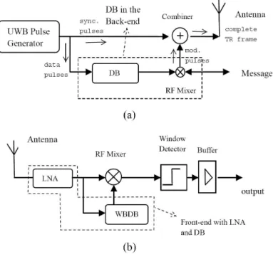
Fig. 1: a) Position of a delay-block in a transmitter employing transmit-reference b) proposed TR receiver front-end including a wideband amplifier and a delay-block.
receiver synchronization when a proper amount of delay is introduced to the received modulated
signal pulses. This temporal shifting is realized with a wideband delay-block (DB) which ultimately
produces a pseudo-template signal for the mixer in the receiver. A simplified model of a TR
transmitter is presented in Fig. 1(a) which includes an UWB pulse generator block (PG) [10]. The
reference or synchronizing (sync.) pulses generated by the PG are delivered to an RF combiner before
being transferred to a transmitting antenna. The particular shape of the wideband pulses usually
resembles that of a monocycle gaussian pulse. The data or message pulses (produced by the same PG)
are delayed by the control mechanism of a delay-block (DB) and a radio-frequency mixer modulates
them with the message signal. The RF combiner merges these modulated and reference pulses to form
a frame for transmission where pulse repetition rate is regulated by the source pulse generator. So, the
back-end of the TR transmitter consists of an RF combiner and a correlating RF mixer. In Fig. 1(b),
the proposed TR front-end which immediately follows the receiving antenna is highlighted. It
produces two responses in the form of a low noise wideband amplifier output and a delayed version of
the received stream from a delay-block (generating a pseudo-pilot signal). The RF mixer in the
receiver is fed with these excitations and the mixer output is processed by a window decision circuit
to recover message bits encoded in the transmitted signal. Ultimately, the CMOS front-end formed
with the matched amplifier and the delay-block plays a crucial role in determining noise performance
and detection accuracy of a TR-receiver. This paper proposes circuit schemes to implement the
Fig. 2: The wideband differential front-end amplifier with cascode half-circuits, RF baluns, and passive matching.
III.
WIDEBAND DIFFERENTIAL FRONT-ENDThis section focuses on the front-end in a TR-receiver which is initiated with a low noise wideband
amplifier with high-gain characteristics. The proposed front-end employs a differential amplifier
to
avail
the benefits of the differential architecture for a transmit-reference receiver circuit. It facilitatesthe RF mixer which is always present in the receiver to adopt a double-balanced structure (like a
Gilbert mixer) and allows the circuit to be differential up to the decision section of its back-end. At
the same time, this topology has to satisfy a relatively high power and area requirement. Despite this
constraint, optimization of device sizes and bias currents keep the power demand for the proposed
amplifier below 15 mW. As the half circuits in the amplifier core and the matching networks are
symmetric in nature they make the architecture more flexible against variation of process. Other
advantages include common mode noise suppression for substrate, greater reduction of power rail
noise, and compatibility with dipole antenna and image rejection techniques. The differential
front-end is also able to achieve a wider range of linear behavior by improving the results of the amplifier’s
second inter-modulation product (IP2) [12]. The proposed amplifier architecture is presented in Fig. 2
with interfacing balanced-unbalanced (balun) circuits. In this topology made with common-source
converted-to-cascode half-circuits, Ld.12 and Ld.22 resonate with the gate-drain parasites of adjoining
transistors (T12 and T22, device ratio: 50µ/0.1µ) and tuning capacitors to define the central operating
frequency. The bias current through the individual half-circuits is controlled by dimension of driving
devices (T11 and T21, aspect ratio: 43µ/0.1µ) and gate biasing voltage (Vgate), resulting in the exclusion
of a separate tail current source in series with the half-circuits. Apart from the reactance Ld.12, the
resonance tank of insulating transistor T12 constitutes a fine-tuning parallel capacitor (Cr.12) and a
small resistor (Rd.12) modeling parasitic resistance contributed by the on-chip inductor. Similarly, Cr.22
devices introduce high resistance to reverse leakage and ensure isolated port operation for matching.
To pre-bias the active input transistors T11 and T21, a bias circuit is formed with the device Tgate (2µ/1
µ) which supplies the dc gate voltage Vgate (= 0.851 V) through a couple of impeding resistors (Rgate1/2
≈5 kΩ). In order to match the input impedance presented by the left-half circuit to 50 in Fig. 2, a
reactiveLC branch (Cin.11andLg.11) is appended with the input gate ofT11 along with a degenerating
source element Ls.11. This branch couples the input driving signal through port RFin1, reduces the
magnitude of imaginary element present in input impedance, and matches the real part of port
impedance to antenna resistance over centered bandwidth. Cin.21, Lg.21 and Ls.21 provide a similar
service for the input device T21 in the right-half of this amplifier circuit. If gm.x is a process
conductance parameter (for transistor x), Cgs.x represents parasitic elements at the gate terminal of
input transistors, and the degenerating inductor Ls.11 is connected with the source of T11, input
interface impedance of the amplifier without any matching can be modeled as [13]
= + ω −
ω .11 .11
.11 .11
.11 .11
1
( ) m s ( ).
in p s s
gs gs
g L
Z with L j L
C C
(1)
After Ls.11 adjusts real element of input impedance and forward gain, equation (1) is modified with the
addition of Lg.11 in the input circuit
= + ω + ω −
ω .11 .11
.11 .11 .11 .11
.11 .11
1
( , ) m s ( ).
in p g s s g
gs gs
g L
Z wit h L L j L L
C C
(2)
The final equation for input impedance matching is achieved after the LC branch is expanded with the
coupling capacitor Cin.11
= = + ω + − +
ω
/ .11 .11
. .11 .11 .11
.11 .11 .11
1 1 1
[ ( ) ( )].
m s
diff left in s g
gs in gs
g L
Z Z j L L
C C C
(3)
Input matching reduces the reactive components and modifies this expression to match it with Rant
which is the antenna resistance preceding the front-end amplifier. A similar expression can be derived
for the right-half of the differential amplifier circuit. A balun-block will be necessary at the RFin.1/2
ports for single to double ended signal conversion at amplifier input ports. Three coils (Lb.4-6) in a
transformer formation execute this balanced to unbalanced transformation process with coupling
parameters K45/46.
Among the active devices of the amplifier, T11 and T21 are responsible for a significant share of
thermal-noise. To emphasize this point, we may define a noise factor (NFdrive) for noise induced at
gate and drain terminals of the driving transistors. The noise components for these devices are its channel noise factor (Niquist factor) , gate terminal noise coefficient , correlation factor between drain and gate noise cogd, and effective quality factor of the input stage Qinp. NFdrive also depends on
amplifier center frequency ( o) and unity-gain transit frequency of transistors ( T ) [14]:
+ ω
σ ξ δ ξ δ
= + − +
ξ σ σ ω
2
2 2 (1 )
1 1
1 [ 2 ] ,
5 5
in p o
drive gd
in p in p in p T
Q
N F co
Q Q Q (4)
m 11
do 11
g g
ξ = . .
, (5)
with gm.11 = input device transconductance and gdo.11 = zero-bias drain conductance of T11. Accounting
influence of driving source impedance (Rs) and gate-source inductors of input transistor, input quality
factor in equation (4) can be defined as
ω +
= o( g.11 s.11). in p
s
L L
Q
R (6)
As expression of noise factor for a driving device has components accounting for drain noise, gate
noise, and correlation between the two terminals and components containing in this equation have
opposing polarities, they are exploited through an optimization process to reduce the noise factor. Noise components for NFdrive also include series resistance contributed by the inductor Lg.11 (Rg.11),
gate-resistance of the input device (Rgate.11), and a process factor which is proportional to the square of
input quality factor (Qinp2) [15]. Hence NFdrive can be expressed with another function with the form of
ω σ χ
= + + +
ξ ω
.11 .11
1 g gat e ( o ),
drive
s s in p T
R R
N F where
R R Q (7)
ξ δ ξ δ
χ = − + +
σ σ
2 2
2
1 2 (1 ).
5 5
gd in p
co Q (8)
Typical values for these process dependent device parameters can be modeled as =0.667, δ=1.33,
ξ=1, and cogd= .39j for long channel devices and =2.5, δ=5, ξ=1, and cogd= .4j for short channel
devices [16], [17]. After canceling out the undesired elements in equation (4) with the optimization
process (which keeps the power dissipation below a fixed limit), expression for minimum noise factor
is simplified to two noise components (conductance ratio ξ and channel noise factor δ) apart from
the operating amplifier frequencies
ω σ = +
ξ ω m in .pdiss 1 2.4 ( o).
T
N F (9)
For limited power dissipation and submicron devices, and δ are replaced by suitable device
constants leading to
ω ≥ +
ω m in 1 1.62( o) .
T
N F (10)
The existence of parasitic elements at the node between input and cascode devices makes noise contribution of the cascode transistor T12 significant, which adds on the noise factor of the overall
amplifier. The sources of cascode noise factor (NFcascode) in the proposed amplifier are the estimated
parasitic capacitance associated with the intermediate node between T11 and T12 (Cparam), zero-bias
drain conductance of cascode transistor (gdo.12), secondary device transconductance (gm.12), driving
source impedance (Rs), and a bias dependent parameter ( ϒ12) [18] which lead to
ω = γ ω 2 2 .12 12 .12
4 ( o param ) ,
cascode s do
T m
C
N F R g
g (11)
where Cparam is approximated by
≈ .12+ .11 + .12.
param gs db sb
C C C C (12)
Therefore, an overall noise factor of the left-half section of the amplifier circuit in Fig. 2
can be
right-half amplifier circuit.
For the output matching circuit connected at the amplifier’s left load port (RFout.1), a design
equation can be formulated for the matching components as [19]
= = =
2
* .12
.12 .11 .11
.1
, L o
in out out
load
X
Z Z R
R (13)
= = =
.12 .11 .1 .12 .12
, L o out load C d C o .
or X R R X X (14)
For the load-port matching circuit in the proposed design, ideally Rload.1 = Zmixer(ℜ)= 50Ω and Rout.11
= Zout.11(ℜ) = 113Ω in K-band (at 21.6 GHz). So, from equation (14)
= Ω
.12 75.17 .
L o
X (15)
A similar model equation can be obtained with Co.22, Cd.22, and Lo.22 for the right-half amplifier circuit
as
= = =
.22 .21 .2 .22 .22.
L o out load C d C o
X R R X X (16)
In this half-circuit Rload.2 = 50 , Rout.21 = Zout.21(ℜ) = 112 Ω near 22 GHz and consequently
= Ω
.22 74.13 .
L o
X (17)
As expected, the two symmetrical matching half-circuits produce similar output port impedances (at
RFout1/2) for the overall amplifier. Finally, an output balun block supports the interfacing of the
amplifier with a following delay-block. To generate a direct feed for a double balanced differential
Gilbert mixer, the load ports may also be linked to the mixer RF ports through small impedances. The
three coils for simulating the load-port balun are designated as Lb.1-3 which are linked with carefully
selected coupling constants K12/13. In actual practice, additional fine tuning of reactive components are
necessary in the amplifier circuit to obtain a sound matched response and optimize gain and noise
performance.
IV. THE SYNCHRONIZING DELAY-BLOCK
As shown in Fig. 1(b), a TR-receiver can support self-synchronizing demodulation because it does
not need a separate template signal for the RF correlator (mixer) in its front-end. But to realize this
feature, it will require a delayed version of the received pulse-train through a wideband delay-block
(DB). This delay-block should be able to handle high data rate of reference pulses and regulate them
in a controlled manner. Design criteria warrant compatibility of the delay-block with different
amplifier topologies as it is placed between a low noise amplifier and a radio-frequency mixer in the
receiver chain. Usage of variable delay units have been reported in applications ranging from voltage
controlled oscillators (VCO) to pulse width control systems (PWCL) [20]. But a wideband
delay-block for a TR-receiver demands special focus on minimizing power dissipation as the system needs
to keep the average power density to the lowest permissible level [21]. Moreover, these delay
elements require wideband characteristics to be able to handle pulses with a duration of 10-10 s. The proposed architecture of a divided wideband delay-block (DB) built with 90 nm transistors and
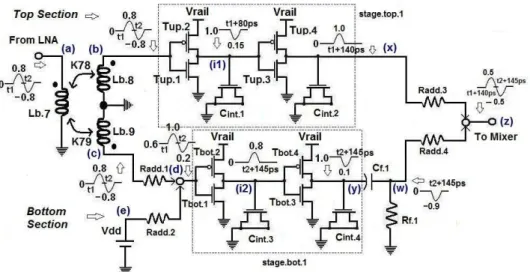
capable of processing bipolar message carrying pulses [22] is presented in Fig. 3. At its input port, the
Fig. 3: The proposed single-stage delay-block (DB) with two parallel branches.
excitations for its top and bottom branches (at nodes b and c). No loss in strength of the input feed
is assumed in the conversion process (ideal coupling). The bottom feed is added with a bias voltage
(Vdd=1.2 V) through a resistive summer to generate an elevated pulse train (at node d). To drive the
delay-block and verify its delay regulation, an 800 mV test signal is applied to the proposed
architecture. The strength of these test pulses can be tuned by adjusting the gain granted by the
preceding amplifier. The primary objective of using two parallel sections in the circuit is to ensure
uniform delay for all member pulses in the driving stream and power the delay block with a single
bias rail (Vrail). For a single-stage DB, as shown in Fig. 3, the sectional delay chains (stagetop.1 and
stagebot.1) are built with a pair of cascaded inverter blocks and two intermediate capacitors. The unit
stagetop.1 is formed with devices Tup.1 (14µ/0.1µ), Tup.3 (1µ/0.1µ), Tup.2/4 (16 µ/0.1µ) and drain-source
shorted transistors contributing junction capacitance (Cint.1=2, in the range of 100 fF ). The driving
stream for the bottom unit (stagebot.1) has a base voltage offset of 0.6 V and a different peak-to-peak
coverage. As a result, it uses transistors with adjusted dimensions {Tbot.1 (20µ/0.1µ), Tbot.3 (8µ/0.1µ),
Tbot.2/4 (16 /0.1 )} and 50 fF shunt capacitors (Cint.3/4). Output from these parallel units (at points x and
y) produces nearly uniform delays for bipolar pulses (average of 180 ps for a single block). In order to
process negative pulses, the driving stream base was elevated to the 0.6 V range at the start of the
bottom unit. As a result, a dc component of 1.0 V is present in the delayed signal at node y of
stagebot.1. This element is removed by an RC branch (made of Rf.1 and Cf.1) and the pulse base is
brought back to near ground level. Radd.3 and Radd.4 form a second resistive summer which combines
the sectional responses to generate a complete delayed pulse train at node z with relatively small
signal dispersion. The overall delay achieved by the proposed single-stage DB is not fixated at 180 ps
but can be fine tuned with a number of design parameters [22], as will be explained in the following
sections.
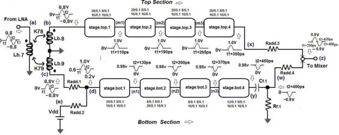
The branched architecture of the delay-block allows extension of numbe
r of stages in each
section (up
to eight) during the testing process. Fig. 4 presents a four-stage wideband delay-blockFig. 4: A complete four-stage delay block (extendable to eight stages).
design. The device sizes (mentioned in the figure) remain consistent for the top section but need to
be adjusted to deal with base elevated pulses in the bottom section. The progress of the delayed pulses
at the intermediate nodes (mi and nj with {i, j}=1-4) is shown in the diagram which indicates a regular
and monotonic variation of achieved delay. The four-stage DB introduces an average overall delay of
~420 ps and the difference in temporal positions of the negative pulse (t2+450 ps at node w and t2+420
ps at point z) can be attributed to the resistive summation process. By controlling gain provided by the
amplifier preceding the delay-block, the strength of input pulses and magnitude of dc offset needed in
the bottom section can be predesigned. Since the wideband pulses are essentially regenerated in this
scheme, no matching circuit will be needed for the delay-block as in the cases of LNA and RF mixer
in the receiver chain. Further discussion on tuning and regulation of the proposed delay-block is
documented in the result section.
The expression for propagation delay achieved by the complete delay chain indicates a non-linear
relationship between overall delay and number of stages or individual delay units in top and bottom
sections. The pair of cascaded inverters in a single-stage branch, as shown in Fig. 3, controls the
component delay with rail voltage (Vrail), shunt reactance (Cint), and device dimensions (W/L ratio)
working as design parameters. For a single inverter gate, the value of saturation current flowing
through the transistors (Isaturation) is considered as average bias tree current and approximated by
= = ( − , ) ,2
2 n
bias saturation gs th n
G
I I V V (18)
where the device (pull-down) threshold level is designated as Vth.n and Gn is transistor
transconductance gain. A mirror equation obtained for the pull-up device will produce the same
magnitude for the bias current. If strength of input pulses and voltage of bias rail are regulated in the
circuit then the following relationship can also be maintained
≈ .
gs rail
V V (19)
After we define tdel.high.low and tdel.low.high as propagation delays for the signal during high-to-low or
low-to-high transition at inverter output and Cshunt as intermediate shunt capacitance, unit inverter-delay
= +
. . . . .
1
( ).
2
del in v del high low del low high
t t t (20)
If Req.p and Req.n represent equivalent resistances when pull-up and pull-down transistors are ’on’, FET
signal transition times will be proportional to time constant of RC networks formed by device (which
is on) resistance and shunt (load) capacitors. When signal drops from high to low at inverter output,
the reactive network is realized with Req.n and output capacitance Cshunt. On the other hand, Req.p
becomes part of this RC circuit in case of low to high transition at gate output. Therefore, propagation
delays can be defined with the functions
=
. . ( ln 2) R . ,
del high low eq n shun t
t C (21)
=
. . (ln 2) R . .
del low high eq p shunt
t C (22)
Using these definitions and expressing ’on’ resistance in terms of transistor sizes lead to [23]
= +
. . .
(ln 2)
(R R )
2
shunt
del inv eq p eq n C
t (23)
≈ ( 1 + 1 )
2
shunt
rail p n C
V G G (24)
= + µ µ ( ), 2 p shunt n
rail ox p p n n L
C L
V C W W (25)
where Cox is unit capacitance of silica layer, µp/n is mobility of carriers, and (W/L)p/n denotes sizes of
concerned transistors. Derivation of equation (32) assumes an insignificant transition time for the
driving signal at the input of the delay-block. In contrast, wideband pulses spend a finite amount of
time to rise or fall at the input node and after this transition time is designated as tup/down,
corresponding delay equations at the output port will be modified as
= +
* 2 2
. . . .
(tdel high low) (tdel high low) (tup/ 2) , (26)
= +
* 2 2
. . . .
(tdel low high) (tdel low high) (tdown / 2) . (27)
Therefore, the final expression of inverter-delay for an individual gate will take the form of
= *+ *
.1. . . . .
1
[( ) ( ) ].
2 o
del stage del high low del low high
t t t (28)
If Cshunt accounts for only design values of intermediate capacitors, external loading capacitance from
a following RF component is modeled as Cextra, input gate capacitance of the delay-block is defined
with Cgate, and equation (28) is modified as
= +
γ
.1. o .1. (1 extra ),
del stage del stage
gate
C
t t
C (29)
where γ(≈1 for a 90 nm process) is a process-dependent proportionality factor. For an M-inverter
N(= 2
M )-stage delay-block branch, the final expression will look like [23]
= +
γ 1 2
. . .1.
( )
(2 ) o [1 N ],
del N stage del st age
F
t N t (30)
delay-block is expected to have three major components [24]. They include a dynamically dissipated power
element (Pdynamic) arising from movement of charge through the shunt capacitor Cshunt at a switching
frequency of fop, a short-circuit power (Psc) component consumed when both transistors in an inverter
gate are on simultaneously with a peak current Imax and conduction duration ton, and a static power
(Pstatic) element dissipated by reverse leakage current Irev.leak. The overall power figure for a complete
wideband delay-block will depend on number of stages used in the delay chain sections, optimized
rail voltage, intermediate capacitance, and finger width of devices. After being processed by the
delay-block, the received signal will leave the front-end and be fed to the following radio-frequency
mixer in the TR-receiver.
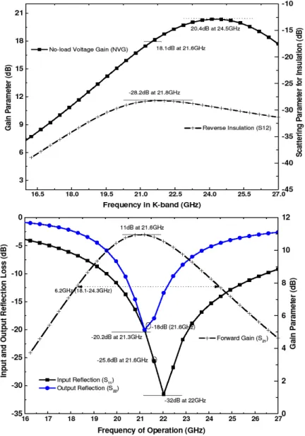
Fig. 5: a) No-load voltage gain and reverse isolation of the front-end around K-band b) forward gain (S21) and port reflection (S11 & S22) parameters.
V. RESULTS AND DISCUSSION
The proposed receiver blocks are designed with an RF simulator including layout parasites
A. Wideband Differential Front-end
As the first section of the proposed TR-receiver front-end, the design parameters of the differential
wideband low noise amplifier are analyzed with the CMOS process. The 90 nm amplifier is able to
achieve high small signal gain and keep noise ceiling and power penalty below 3 dB and 15 mW,
respectively. During parameter extraction, the LNA is interfaced with balun-circuits and a matched 50
load.
1) Forward Gain and Port-Reflection Parameters: The peak voltage gain (PVG) of the differential
low noise amplifier with an open-circuited load-port is 20.4 dB in the K-band (24.5 GHz) and 18.1 dB
at the center frequency (21.6 GHz), as shown in Fig. 5(a). It also shows that resistance to reverse
isolation (S12) is always greater than 28.3 dB and can reach up to 35 dB within the message
bandwidth. In Fig. 5(b), maximum forward gain (indicated by S21) is 11 dB, peaking at 21.6 GHz and
presenting a 3-dB-bandwidth of 6.2 GHz (18.1-24.3 GHz). The same frame plots input and output
port matching parameters (S11 & S22) with minima at -32 dB and -20.2 dB, respectively, in the 21-22
GHz range. The port return loss at the amplifier peak frequency (21.6 GHz) are -25.6 dB and -18 dB,
in that order. Therefore, undesirable port-reflection remains insignificant over the concerned
frequencies for the amplifier.
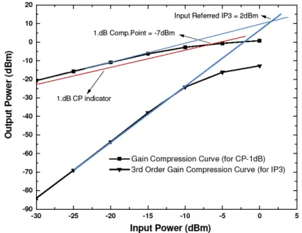
Fig. 6: Linear range of amplifier operation as manifested by input-port referred 1dB-CP and IP3.
2) Estimation of Linear Behavior from the Amplifier: As the power of its driving signal (in dBm) is
raised for the wideband amplifier, the input-referred one-decibel compression point (1dB-CP ) is eventually crossed at -7.24 dBm and the projection modeling the third-order intercept point (IIP3)
intersects the input power axis at 2 dBm before the amplifier enters a non-linear region of gain
compression (see Fig. 6). At the compression point the amplifier is expected to deliver 2 dBm power to
a matched load while still remaining in linear domain and the estimated output power at IIP3 point is
Fig. 7: a) Noise parameters and B1f factor (for amplifier bandwidth) b) power gains provided by amplifier core and matched amplifier accompanied with Rollett (Krollet) factor.
3) Noise: With the employment of a differential topology, the designed front-end is able to
maintain its noise parameters below the ceiling of 3 dB (2.58-2.97 dB). Its projected noise figures (NF
and theoretical NFmin) are documented in Fig. 7(a) which coincide around the center point. NF settles
around 2.58 dB near the center frequency (21.6 GHz) and approaches a minimum peak of 2.5 dB at
the edge of its bandwidth, indicating optimum noise performance over this frequency coverage.
4) Power Gain and Power Penalty: Among an amplifier’s power gain parameters, available gain
(GA) provides an estimation of power gain provided by the core amplifier which is lowered do
wn to
transducer gain (GT
) after the addition of port-matching networks. In Fig. 7(a), GA, GT, and GP(average power gain) coincide near 11 dB around the center frequency which can be interpreted as an
indication of successful port-matching. Maintaining its compatibility with low power on-chip
transceivers, dc power consumed by the font-end is measured as 13.9 mW when amplifier
5) Estimation of Stability (Kf and B1f factors): The amplifier is expected to be behave in an unconditionally stable manner over all frequencies around the message bandwidth. To assess this quality, the microwave stability factor B1f is defined in terms of scattering parameters
= + 2 − 2− ∆2
1f 1 11 22 ,
B S S (31)
∆ =S11S22−S12S21, (32)
which is required to satisfy the following condition
>
1f 0 .
B over t he ban dwidth (33)
When presented in Fig. 7(b), B1f is found to have a magnitude between 0.524 and 0.97 in the
concerned range of bandwidth (18.1-24.3 GHz). To verify this result with a second stability parameter, the Rollett stability factor (Krollet) is also plotted in the same figure with its value always
being greater than a unit limit (fulfilling its criterion of stability) [13]. This factor is also defined with
s-parameters
− − + ∆
=
2 2 2
11 22
21 12
1 2 rollet
S S
K
S S
(34)
and has a relatively flat profile (3.71-3.82) with a lowest trough of 3.707 at 21.6 GHz. As a result, the
amplifier will provide resistance to oscillation induced by white noise which may get accumulated in
the circuit during its start-up mechanism.
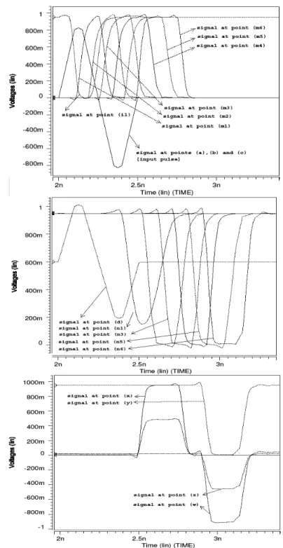
B. Wideband Delay-Block (DB)
The proposed wideband delay-block (DB) to follow the front-end amplifier is also built with 90 nm
CMOS devices as a part of the TR-receiver architecture. To illustrate the progression of a driving
bipolar pulse stream through a multi-stage delay chain, a six-stage delay-block (built with the same
principle presented in Fig. 4) is subjected to a pulse train of monocycle gaussian pulses. Fig. 8(a)
presents the time domain signals existing at different nodes of the top section for a complete six-stage
DB. Delayed versions (130-500 ps) of the positive half of the input pulse are collected from output
nodes (m1-m6) of six successive stages (See Fig. 4) and a sample intermediate node (i1) in the first
stage of the delay chain. A symmetric balun produces identical replicas of the the driving pulse and
feed them as sectional inputs (at points b and c). In Fig. 8(b), after the input pulse is elevated with a
bias voltage (Vdd) for the bottom section, the driving signal is now collected from point d. Delayed
versions for the elevated negative-half of the input signal show a progression of 150-650 ps at output
nodes of stages in the bottom section (n1-n6). The final response (at node y) gathered after six stages in
the bottom section is decoupled (dc component removed) at node w as shown in Fig. 8(c). It also
shows the signal produced by the output combiner (culminating at node z) which manifests an average
delay of 620 ps. Similar number of stages are employed in the DB branches to achieve identical and
uniform delay for all pulse elements. The responses demonstrate that monotonic and quasi-linear rise
Fig. 8: Progression of delayed response as achieved through a six-stage delay-block at different points a) for top section b) for bottom branch c) overall response.
(W/L)p.(up/bot).q is selected as the notation to define dimension of individual transistors and Cp.int.q
expresses value of a shunt DB capacitor where p=1-6 are stage indices of delay sections and q=1-4
indicate individual transistors or capacitors for a particular stage. To produce the response in Fig. 8,
Vrail is set to 0.95 V and dimensions of the first stage are selected as
= 14 = 1
( )1. .1 , ( )1. .3 ,
0.1 0.1
W W
up up
L L (35)
= 20 = 8
( )1. .1 , ( )1. .3 ,
0.1 0.1
W W
bot bot
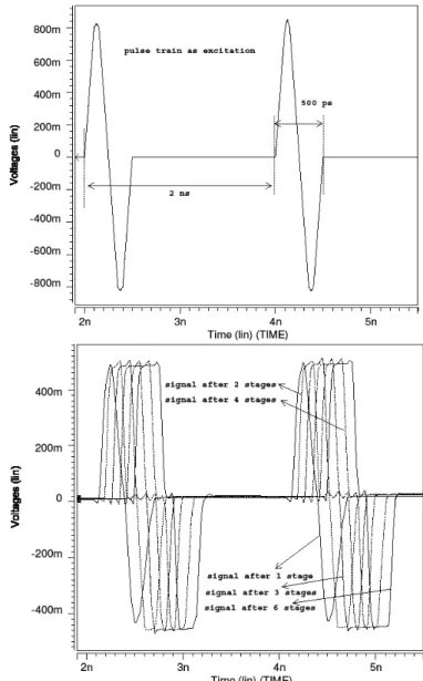
Fig. 9: a) Input wideband pulse stream of monocycle gaussian pulses b) delayed versions at the final output port of the delay-block while varying the number of stages.
= = = = 16
( )1. .2 ( )1. .4 ( )1. .2 ( )1. .4 .
0.1
W W W W
up up bot bot
L L L L (37)
The other five stages require manipulation of device dimensions to compensate for any signal drop at
intermediate nodes. Power dissipated by a single-stage delay-block is kept below 9 mW and for a
six-stage delay unit power penalty reaches up to 10.6 mW. According to design requirement, number of
stages in the DB can be varied to achieve regulated temporal shifts. The signal typically collected by a
TR-receiver front-end is shown in Fig. 9(a) in the form of a wideband pulse stream made with
monocycle gaussian pulses. Fig. 9(b) presents its delayed versions collected from the output ports of
the proposed multi-stage delay-block. In addition to the number of stages in a DB section, tuning of
delay may also be controlled by shunt capacitors, ratio of transistors, and magnitude of rail voltage
[22]. This phenomenon is further illustrated in tabular form for a single-stage delay-block in the
VI. SUMMARY OF PERFORMANCE
A. Front-End Amplifier
The synopsis of simulated performance extracted from the proposed differential front-end is
summarized in Tables I and II where it is compared with simulated results of published wideband
amplifier circuits [25]-[32]. To enable relative evaluation of amplifiers built on different scales of
CMOS technology, a composite FOM (figure-of-merit) parameter is defined as
=
− 21
m in
( ) .( )
.
( ) { ( ) 1}
S dB C en ter Freq G Hz FO M
P ower m W N F dB (38)
In summary, the proposed amplifier achieves a better figure of merit (10.5) and realizes a 22 GHz TR
front-end customized for low-NF (2.6 dB) high-gain (11 dB) moderate power (13.9 mW) applications.
B. Delay-Block
The literature on the proposed delay-block has estimated that tuning of shunt capacitors and
transistor dimensions will raise the group-delay achieved by the chain and increasing the rail voltage
will have an opposite effect. To verify these predictions, performance of a single-stage delay-block
under regulation is summarized in Table III where its specified controlling parameters (including
number of cascaded stages) are varied. Among the four shunt capacitors of a single-stage DB, C1.int.1
provides fine tuning (range of 50 ps) while other reactances are set to fixed values (C1.int.3=C1.int.1 and
C1.int.4=C1.int.2=50 fF). Progression of bipolar peaks through the delay-block becomes non-uniform
when device dimension is varied as their negative peak suffers from higher group dispersion. In Table
III, W1.up.1 and L1.up.1 are manipulated as control figures for a delay variation of 150 ps whenW1.up.3=8
µm and W1.up.2=W1.up.4=16 µm. The third control parameter of the DB (rail voltage, Vrail) achieves a
range of delay regulation which is nearly 200 ps. With total number of stages varying between one
for the delay-block has a fixed component (7 mW) for summer circuits and the remaining power
element (peak) varies between 1.5 and 3.6 mW as eight stages are cascaded in both sections of the
delay chain.
VII. CONCLUSIONS
This paper proposes circuit-level implementation of a 22 GHz 90 nm CMOS receiver front-end
suitable for the principle of transmitted-reference (TR) communication. Using an LC port-matching
technique, the front-end amplifier realizes a differential topology with high simulated gain (11 dB) to
improve system noise performance (below 3 dB). Base NF ceiling for the wideband amplifier is
expected to be 2.6 dB and the circuit consumes 13.9 mW when driven from a 1.2 V bias rail. Over its
6.2 GHz bandwidth, reverse isolation for the front-end is better than the margin of -28 dB with
minimum port-matching parameters of -32 dB and -20.2 dB, respectively. A wideband 90 nm
delay-block (DB) completes the CMOS front-end which is capable of producing a delayed version of the
regulation of bipolar delay in the range of 70-800 ps is attained with four control parameters.
Comparison with simulated reported designs establishes a superior figure-of-merit for the front-end
amplifier and along with the delay-block it would complement the realization of a TR transceiver in
circuit level.
VIII. ACKNOWLEDGMENT
The author would like to thank S. Rashid, Dr. H. Rashid, and the Dept of EEE of Bangladesh Univ.
of Engineering and Technology.
REFERENCES
[1]M. Sun, Y. P. Zhang, G. X. Zheng, W.-Y. Yin, ”Performance of Intra-Chip Wireless Interconnect Using On-Chip Antennas and UWB Radios,” IEEE Trans. Antennas and Propagation, Vol. 57, No. 9, pp. 2756-2762, Sept. 2009. [2]I.E. Lager, A.T. De Hoop, ”Inter-chip and intra-chip pulsed signal transfer between transmitting and receiving loops in
wireless interconnect configurations,” in Proc. European Microwave Conf., pp. 577-580, Sept. 2010.
[3]M.F. Chang, V. Roychowdhury, L. Zhang, H. Shin, Y. Qian, ”RF/wireless interconnect for inter- and intra-chip communications,” Proceedings of the IEEE, Vol. 89, No. 4, pp. 456-466, Apr 2001.
[4]W. Malik, C. Stevens, D. Edwards, ”Multipath Effects in Ultrawideband Rake Reception,” IEEE Trans. Antennas and Propagation, Vol. 56, No. 2, pp. 507-514, Feb. 2008.
[5]Rashid H., Watanabe S., Kikkawa T.: ‘Characteristics of Si Integrated Antenna for Inter-chip Wireless Interconnection’, Japanese Journal of Applied Physics, 2004, 43, (4B), pp. 2283-2287.
[6]Saha P. K., Sasaki N., T. Kikkawa: ‘A CMOS Monocycle Pulse Generation Circuit in a Ultra- Wideband Transmitter for Intra/Inter Chip Wireless Interconnection’. Japanese Journal of Applied Physics, 2005, 44, (4B), pp. 2104-2108. [7]Goeckel D.L., Qu Z.: ‘Slightly frequency-shifted reference ultra-wideband (UWB) radio: TR-UWB without the delay
element’, Proc. Military Communications Conference, MILCOM, 2005, pp. 3029-3035.
[8]Roy S., Forester J.R., Somayazulu V.S., Leeper D.G.: ’Ultrawideband radio design: the promise of high speed, short-range wireless connectivity,’ Proc. of the IEEE, 2004, 92, (2), pp. 295-311.
[9]FCC regulation on ultra-wideband radio. [online]. Available: http://hraunfoss.fcc.gov/edocs public/attachmatch/FCC-02-48A1.pdf, accessed June 2011.
[10]Hoctor R. T., Tomlinson H. W.: ‘Delay-Hopped, Transmitted Reference RF Communications,’ Proc. IEEE Conf. On UWB Systems and Technologies, 2002, pp. 265-270.
[11]Casu M.R., Durisi G.: ’Implementation aspects of a transmitted-reference UWB receiver’, Journal of Wireless Communications and Mobile Computing, 2005, 5, (5), pp. 551 - 566.
[12]H. K. Chiou, H. Y. Liao, K. C. Liang, Compact and low power consumption K-band differential low-noise amplifier design using transformer feedback technique, IET Microwaves, Antennas and Propagation, vol.2, no.8, pp.871-879, Dec. 2008.
[13]Leung B.: ‘VLSI for Wireless Communication’, (Prentice Hall India, New Delhi, 2002, 1st Ed.).
[14]D. K. Shaeffer and T. H. Lee, ”A 1.5-V, 1.5-GHz CMOS low noise amplifier,” IEEE J. Solid-State Circuits, vol. 32, no. 5, pp. 745-759, May 1997.
[15]T. K. Nguyen, C. H. Kim, G. J. Ihm, M. S.Yang, and S. G. Lee, ”CMOS low-noise amplifier design optimization techniques,” IEEE Trans. Microw. Theory Tech., vol. 52, no. 5, pp. 1433-1442, May 2004.
[16]A. van der Ziel, ”Noise in solid-state devices and lasers,” Proc. IEEE, vol. 58, no. 8, pp. 1178-1206, Aug. 1970. [17]D. K. Shaeffer and T. H. Lee, ”Comment on Corrections to a 1.5-V, 1.5-GHz CMOS low noise amplifier,” IEEE J.
Solid-State Circuits, vol. 41, no. 10, pp. 2359-2359, Oct. 2006.
[19]Rashid S, Roy A, Ali N, Rashid H., Design of a 21 GHz UWB Differential Low Noise Amplifier using .13 m CMOS Process., Proc. of 12th Int. Symp. on Integrated Circuits, 2009, p. 538-41.
[20]Eto S., Akita H., Isobe K., Tsuchida K., Toda H., Seki T.: ‘A 333MHz, 20mW, 18ps resolution digital DLL using current controlled delay with parallel variable resistor DAC (PVR-DAC),’ Proc. 2nd IEEE Asia Pacific Conf. on ASIC, 2000, pp. 349–350.
[21]Terada T., Yoshizumi S., Sanada Y., Kuroda T.: ‘Transceiver circuits for pulse based ultra-wideband,’ Proc. of International Symposium on Circuits and Systems, 4, May 2004, pp. 349-352.
[22]Roy A., Rashid S., Arafat M.A., Rashid H.: ’Design of a Wideband Delay Element for Transmitted Reference UWB Receivers’, Proc. Int. Conf. on Electrical and Computer Eng. ICECE, December 2010, pp. 97-100.
[23]Rabaey J.M., Chandrakasan A., Nikolic B.: ‘Digital integrated circuits: A design perspective’. (Prentice-Hall India, New Delhi, 2nd ed., 2003)
[24]N. R. Mahapatra, A. Tareen, S. V. Garimella, Comparison and Analysis of Delay Elements. Proc. 45th Midwest Symposium on Circuits and Systems, Aug. 2002. p. 473-476.
[25]Guo X, O KK, A Power Efficient Differential 20GHz Low Noise Amplifier With 5.3GHz 3dB Bandwidth. IEEE microwave and wireless components letters, 2005; 15:603-5.
[26]Yu YH, Chen Y, Heo D, A 0.6-V low power UWB CMOS LNA, IEEE Microw. Wireless Compon. Lett. 2007; 17:229-31.
[27]Zhang F, Kinget FR. Low-power programmable gain CMOS DA. IEEE J. Solid-State Circuits 2006, 41:1333-43. [28]Wang RL, Lin MC, Yang CF, Lin CC. A 1 V 3.1-10.6 GHz full-band cascoded UWB LNA with resistive feedback.
Proc. of IEEE EDSSC Conf., 2007, p. 1021-23.
[29]B. Welch et al., ’A 20-GHz low-noise amplifier with active balun in a 0.25. m SiGe BICMOS technology’, IEEE J. Solid-State Circuits, vol. 40, no.10, pp. 2092-2097, Oct. 2005.
[30]S. C. Baakmeer, E. A. M. Klumperink, B. Nauta, and D. M. W. Leenaerts, ’An inductorless wideband balun-LNA in 65 nm CMOS with balanced output,’ in Proc. ESSCIRC, 2007, pp. 364-367.
[31]T. Chang, J. Chen, L. Rigge, and J. Lin, ’A packaged and ESD-protected inductorless 0.18 GHz wideband CMOS LNA,’ IEEE Microw. Wireless Compon. Lett., vol. 18, no. 6, pp. 416-418, Jun. 2008.