Abstract—A balanced-to-single-ended (BTSE) Wilkinson power
divider of planar microstrip structure is proposed in this paper. It has a balanced input and two single-ended outputs. Cascade of a balun and a conventional power divider can be replaced by this proposed structure. Based on the theory of mixed-mode S parameters and the admittance matrix method, the critical parameters are determined. The four-port network is analyzed by simplifying it to two-port network with other ports matched at the central frequency. Then the key parameters are derived and the impact of a freely selected variable on the bandwidth is also discussed. An example of 2.4GHz BTSE power divider is designed. The simulated and measured results show the effectiveness of the method: differential-mode transmissions are better than -3.25dB, mode transmissions are lower than -28.6dB, common-mode return loss is -0.10dB, differential-common-mode return loss and isolation is lower than -23.7dB. While the operating bandwidth is 20%.
Index Terms—balanced circuit; power divider; mixed-mode S-matrix
I. INTRODUCTION
Balanced RF circuits have more advantages than single-ended ones. The most important advantage is the ability of anti common-mode interference. As power divider is an important microwave/millimeter wave passive device, scholars have made a deep research on balanced power dividers [1-7].In [1], a wide band miniature balanced power divider is designed with the coupled lines. Then a balanced Wilkinson power divider with microstrip structure was presented [2], it contains four lumped resistors which affect the performance when working at high frequency. Later, some scholars improved the structure by using two resistors [3]. Further in [4], the lumped resistors were reduced to one. By using half-mode substrate integrated waveguide (SIW) structure, a balanced symmetric Gysel power divider is designed [5]. Also, balanced Gysel power divider with arbitrary power division ratio [6] and dual-band balanced Wilkinson power divider [7] are designed.
As mentioned above, these studies are all about the balanced-to-balanced (BTB) power divider, but in some modern practical applications, it may demand a power divider which contains both single-ended port and balanced port, such as when the signals received by a balanced antenna need to be processed by single-ended receivers [8] or when the differential power amplifier need to be connected
A Balanced-to-Single-Ended Wilkinson
Power Divider
Zhen Yang1, Weiguo Liu2
1
School of Electronic and Optical Engineering, Nanjing University of Science and Technology, Nanjing, China 2
Zhejiang Key Lab of Automobile Safety Technology, GEELY AUTOMOBILE RESEARCH INSTITUTE, Hangzhou, China, [email protected], [email protected]
Chen Miao3, Xin-an Yuan4, Wen Wu5
3-5
to a single-ended antennas to work in a radar system effectively [9]. Research in this area is relatively few. A BTSE power divider is designed with double-side structure [10], which brings inconvenience to practical application. [11] proposed a BTSE power divider with filtering function, however, the operating bandwidth of it is less than 7%.
In this paper, the relationship between mixed-mode S-matrix and traditional S-matrix of the four port network of the proposed power divider is analyzed and derived, then a transformation is introduced to simplify the design process. At last, based on the mixed-mode S parameters theory and the admittance matrix method of the two-port balanced network, a new BTSE power divider with planar microstrip structure is proposed. And its performances are demonstrated by the simulated and measured results. The impact of a freely selected variable on the bandwidth is also discussed.
II. ANALYSIS AND DERIVATION OF KEY PARAMETERS
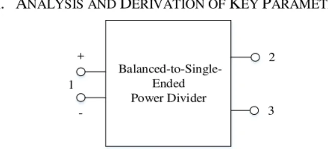
Balanced-to-Single-Ended Power Divider +
-2
1
3
Fig. 1. Schematic diagram of a three port BTSE power divider
As shown in Fig.1, a three port BTSE power divider transmit the input signal from balanced port 1 to single-ended ports 2 and 3. In the research of balanced circuit, we often use mixed-mode S-matrix to replace the traditional S-matrix. Its mixed-mode S-matrix is
SS SC SD
CS CC CD
DS DC DD
SS SS SC SD
SS SS SC SD
CS CS CC CD
DS DS DC DD
M
S S S
S S S
S S S
S S S S
S S S S
S S S S
S S S S S
33 32 31 31
23 22 21 21
13 12 11 11
13 12 11 11
(1)
In this matrix, SXYijmeans the S-parameter when port j is in Y mode excitation and port i is in X
mode response, where X, Y are corresponding to differential mode (D), common mode (C) or
single-ended mode (S), while i, j are corresponding to port 1, port 2 or 3. At the same time, SXY represents
the corresponding matrix block.
Typically, the parameters should meet the following conditions:
1) The power divider should be reciprocal, so its mixed-mode S-matrix is symmetric (SXYij SYXji); 2) Each port should be matched to the differential signal, at the same time, single ports are also
matched (SDDii0andSSSii0);
3) The input common mode noise should be fully reflected, with no mutual conversion between the
4) The output ports should be isolated from each other( SSS23 0andSSS32 0).
According to these, the desired mixed-mode S-matrix of the power divider with equal power division will be:
0 0 0 2 / 2 0 0 0 2 / 2 0 0 0 2 / 2 2 / 2 0 0 2 1 3 2 1 j j j j M e e e e e S j (2)where1,2,3 are the phase shift of the S-parameters. To the BTSE power divider in this
paper,1,2,3are set to 1/2,2 /2,3.So we can get the mixed-mode S-matrix:
0 0 0 2 2 0 0 0 2 2 0 0 1 0 2 2 2 2 0 0 j j j jSM (3)
In order to get the traditional S-matrix to derive the key design parameters, we need to know the transformation between mixed-mode S-matrix and traditional S-matrix. To simplify the calculation, we rearrange the traditional S-matrix: Supposing a network containing N balanced ports and M single ports, the traditional S-matrix is rearranged as this block matrix:
N N cc N N cb M N ca N N bc N N bb M N ba N M ac N M ab M M aa S S S S S S S S S S (4)where a,b,c respectively represents the single-ended port, the positive end of the balanced port and the negative end of the balanced port.
Based on these and derivation of the relationship between mixed-mode matrix and traditional S-matrix in [12], we can get:
2 1 S CC DC CD DD CC DC CD DD CS DS CC DC CD DD CC DC CD DD CS DS SC SD SC SD SS S S S S S S S S S S S S S S S S S S S S S S S S S ) ( 2 ) ( 2 ) ( 2 ) ( 2 2 (5)So we can get the traditional S-matrix to the BTSE power divider in this paper:
2 1 2 1 2 1 2 1 2 1 2 1 2 1 2 1 2 1 2 1 0 0 2 1 2 1 0 0 1 1 1 1 31 31 1 1 1 1 21 21 3 1 2 1 33 32 3 1 2 1 23 22 j j j j j j j j S S S S S S S S S S S S S S S S S (6)1+
1-2
3 Z1,θ1
Z2,θ2
Z3,θ3
Z4,θ4
R1
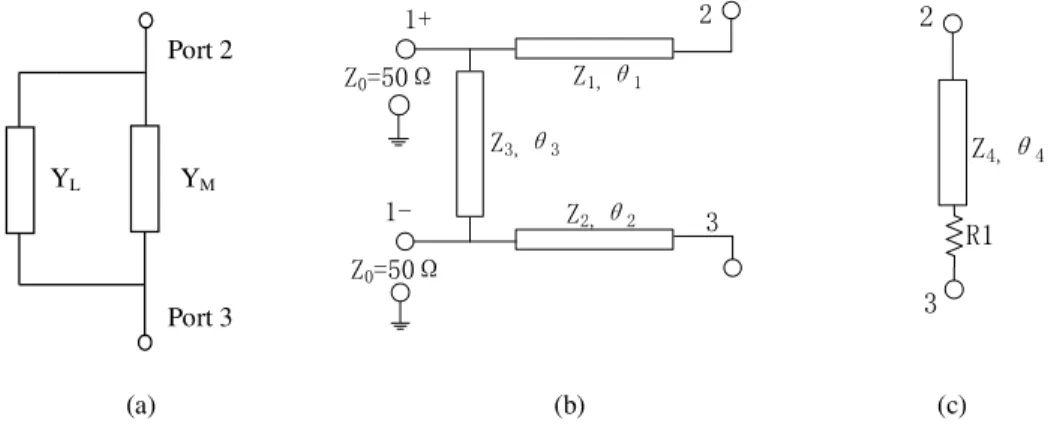
Fig. 2. Structure of the BTSE power divider
As shown in Fig.2, this BTSE Wilkinson power divider consists of four transmission lines and a
resistance with the electrical lengths of the transmission lines are 12 2and 34. While Z1,
Z2, Z3, Z4 and R1 are to be determined. All the four ports have the same port impedance ofZ050. In order to determine the critical parameters, the structure is analyzed by simplifying it to two-port network with other ports matched at the central frequency. As shown in Fig.3,
Port 3
YL YM
Port 2
1+
1-2
3 Z1,θ1
Z2,θ2 Z3,θ3 Z0=50Ω
Z0=50Ω
2
3
Z4,θ4
R1
(a) (b) (c)
Fig. 3. Network between 2 and 3:(a) The equivalent network between port 2 and 3;(b) The circuit represented by YL;(c) The circuit represented by YM
using (6) we get:
0 0
0 0 33 32
23 22 23
S S
S S
S (7)
According to (7) and the relationship between S-matrix and admittance matrix, we have:
0 0 23
0 0
Y Y
Y (8)
whereY0 150 1
is the admittance of each port. The admittance matrix of the network can also be
expressed as:
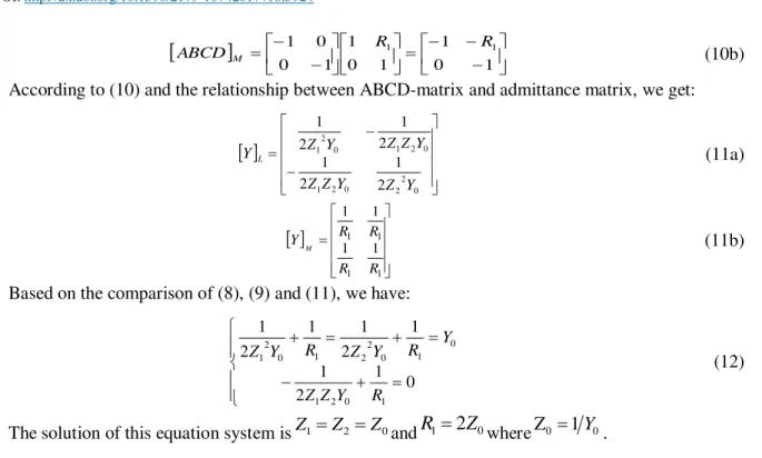
Y23YLYM (9)Based on Fig.3 (b) and (c) we can get theirs ABCD matrix:
1 2
0 2 1 2 1
2 2
0 0
1 1
0 2
0 0 1 0 1 1 0
0 1 1 0 1 0 0
Z Z
Y Z Z Z Z
jY jZ Y
Y jY
jZ
1 0
1 1
0 1 1 0
0
1 R1 R1
ABCD M (10b)
According to (10) and the relationship between ABCD-matrix and admittance matrix, we get:
0 2 2 0 2 1
0 2 1 0
2 1
2 1 2
1
2 1
2 1
Y Z Y Z Z
Y Z Z Y
Z
YL (11a)
1 1
1 1
1 1
1 1
R R
R R Y
M (11b)
Based on the comparison of (8), (9) and (11), we have:
0 1 2
1
1 2
1 1 2
1
1 0 2 1
0 1 0 2 2 1 0 2 1
R Y Z Z
Y R Y Z R Y Z
(12)
The solution of this equation system isZ1Z2Z0andR12Z0whereZ01Y0.
From the above results, we can know that Z3 and Z4 can be freely selected. In this paper, we set
x
Z Z
Z3 4 at central frequency. Next, the impact of the freely selected variable Zx on the relative
bandwidth (BW) of the power divider will be introduced.
From the above discussion, we can know that the parameters in the matrix blocksSSS,SCS,SDD
(isolation, common-mode rejection, and differential-mode return loss) mainly determine the performance of the power divider. We define the minimum relative bandwidth of these parameters as the relative bandwidth of the power divider. Fig.4 presents the Zx in the range of (20Ω< ZX <200Ω), with the relative bandwidth with the trend of Zx change. It can be seen when the Zx is equal to 60Ω, the power divider get the maximum relative bandwidth of 27.5%. We take Zx50 as an example to realize and test the proposed power divider.
Fig. 4. Relationship Between Zx and the relative bandwidth
III. REALIZATION OF BTSEPOWER DIVIDER
According to the above analysis and design, a balanced-to-single-ended power divider is realized,
0027 . 0
tan . The operating band is centered atf02.4GHz. The positive and negative terminals of
the balanced input port 1 are located on the left, while the two single-ended outputs are on the right. The geometric parameters in Fig.5 are L=12 mm, L1=18.5 mm, L2=37 mm, L3=12 mm, W1=1.13 mm, W2=1.13 mm, W3=1.13 mm, g=1.2 mm.
Fig. 5. Photo of the BTSE power divider
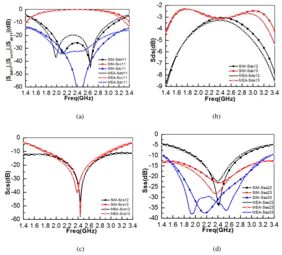
Finally, the simulated results and measured results obtained by Ansoft HFSS and Aglient E5071 are all shown in Fig.6.
(a) (b)
(c) (d)
Fig. 6.Simulated and measured results of the BTSE power divider prototype:(a) Parameters of balanced port 1;(b) Differential mode transmission parameters Sds;(c) Common mode transmission parameters |Scs|;(d) Return loss and isolation
As we can see, good performances have been successfully achieved with the proposed BTSE power divider. At center frequency 2.4GHz, the measured differential-mode transmissions are: |Sds12|=3.25dB, |Sds13|=3.17 dB; commonmode transmission parameters |Scs12|, |Scs13| are respectively -30.5dB and -28.6dB; differential-mode return loss of port 1 is |Sdd11|=-25.1 dB while common-mode return loss is |Scc11|=-0.10dB; the return loss of ports 2 and 3 are |Sss22|=-22.3dB, |Sss33|=-32.4dB; isolation parameters between 2 and 3(|Sss23|)is -23.7dB. The common-mode transmissions, the differential-mode return loss, the return loss of ports 2 and 3, the isolation between 2 and 3 are all lower than -15dB between 2.16 GHz~2.61 GHz. The relative bandwidth is 20%. Due to the error of the device fabrication and parameter testing, the experimental results and the simulated results have some differences in some parameters (Sdc11 and Sss33). Except this, the simulated results and the experimental results are in good agreement.
IV. CONCLUSION
Balanced-to-single-ended power divider makes up for the lack of performance when connect balanced devices and single-ended devices in many systems, and the research of this power divider is particularly important. A BTSE Wilkinson power divider of planar microstrip structure is proposed, investigated, and fabricated in this paper based on the theory of mixed-mode S parameters and the admittance matrix method. At center frequency 2.4GHz, differential-mode transmissions are|Sds12|=3.25dB, |Sds13|=3.17 dB, commonmode transmissions|Scs12|, |Scs13|are respectively 30.5dB and -28.6dB, common-mode return loss|Scc11|is -0.10dB, differential-mode return loss is|Sdd11|=-25.1 dB, isolation|Sss23|is -23.7dB. The 15dB relative bandwidth is about 20%. The simulated and measured results show its great merits of low insertion loss, good return loss, high isolation and high common-mode rejection (common-common-mode transmissions).Therefore, power divider designed in this paper can meet the requirements of most radar and communication systems.
ACKNOWLEDGMENT
This work is supported by Foundation of Zhejiang Province Key Laboratory of Automobile Safety and Opening Foundation of Jiangsu Key Laboratory of Spectral Imaging and Intelligent Sense.
REFERENCES
[1] J. W. May and G. M. Rebeiz, A 40-50 GHz SiGe 1:8 differential power divider using shielded broadside-coupled striplines[J], IEEE Transactions on Microwave Theory and Techniques, Jul. 2008, 1575–1581,
[2] B Xia, L S Wu, and J F Mao. A new balanced-to-balanced power divider/combiner[J], IEEE Trans. Microw. Theory Techn, Sep. 2012: 287–295.
[3] M J Park. Comments on ‘A new balanced-to-balanced power divider/combiner’ [J], IEEE Transactions on Microwave Theory and Techniques, Feb. 2013, 1000-1000.
[4] B Xia, L S Wu, and J F Mao. Authors’ reply[J], IEEE Transactions on Microwave Theory and Techniques, Feb. 2013,
1001–1003.
[5] L.S. Wu, B. Xia, and J. F. Mao. A half-mode substrate integrated waveguide ring for two-way power division of balanced circuit[J], IEEE Microw.Wireless Compon. Lett. , Jul. 2012: 333–335.
[6] B. Xia, L.-S. Wu, and J. F. Mao. A Balanced-to-Balanced Power Divider With Arbitrary Power Division[J], IEEE Transactions on Microwave Theory and Techniques, Aug. 2013, 2831-2840.
[7] B Xia and J F Mao, A new dual-band balanced-to-balanced power divider[J], Progr. Electromagn, Jan. 2013, 53–66. [8] S. B. Grković, "Small balanced antennas for Bluetooth applications," MELECON 2014 - 2014 17th IEEE
[9] A. R. Ghorbani and M. B. Ghaznavi-Ghoushchi, "A 35.6dB, 43.3% PAE class E differential power amplifier in 2.4GHz with cross coupling neutralization for IoT applications," 2016 24th Iranian Conference on Electrical Engineering (ICEE), Shiraz, 2016, pp. 490-495.
[10]L S Wu, Y X Guo, J F Mao. A New Balanced-to-Single-Ended (BTSE) Power Divider[J],Wireless Symposium (IWS),
2014 IEEE International,March 2014, 1 – 4.
[11]K. Xu, J. Shi, L. Lin, and J.-X. Chen, "A Balanced-to-Unbalanced Microstrip Power Divider With Filtering Function," IEEE Trans. Microw. Theory Techn., vol. 63, no. 8, Aug. 2015, pp. 2561 – 2569.
[12]CHEN Yin-chao, YANG Shu-hui. Mixed mode S-parameters for applications of RF differential networks[J], Journal of