Abstract— In this study, a novel microstrip fed Ultra Wideband
(UWB) antenna is presented. The proposed antenna, with a size of 26×30×1.6mm3, is capable of removing four bands of interference in the coverage band. Firs, three filtered bands are created by cutting U, L, and C-shapes, a horizontal line on the patch, and fed line of antenna. The fourth notch is created by a new method that involves the use of a metalized via-hole and a C-shaped strip line in the rear side of the radiation patch. In the next step, the proposed antenna is compared with similar models with regard to different features such as size, bandwidth, and the number of the filtered frequency bands, in a new framework based on the Analytic Hierarchy Process. Thus, with a comprehensive comparison, the functional aspects of the proposed antenna are presented. The characteristics of the proposed antenna, such as radiation pattern, gain, and return loss (S11<-10dB), were measured; the correspondence between the simulated and measured results was acceptable.
Index Terms— Analytical hierarchy Process, ultra-wideband antenna, L-shaped slot antenna, U-L-shaped slot antenna
I. INTRODUCTION
Recently, researchers developed ultra-wideband (UWB) systems with the aim of achieveing wider operating bandwidth, high speed data, lower power spectrum, etc. [1]. The restriction of UWB frequency spectrum (from 3.1 to 10.6GHz) by Federal Communications Commission (FCC), directed
researchers’ attention toward using UWB communication systems, and many monopole antennas with
different patches or slots were considered for UWB systems [1]. Nevertheless, the design of UWB systems is still facing many challenges [2]. For rinstance, in case of covering wider bandwidth, UWB systems could easily be interfered with the adjacent systems such as the wireless local area networks (WLANs) operating in the IEEE WiMAX network 3.35-GHz (3.3–3.4 GHz), 3.5-GHz (3.4–3.6 GHz), 3.7-GHz (3.6–3.8 GHz) (5.725–5.85 GHz), WLAN 5.25-GHz (5.15–5.35 GHz) and 5.75-GHz (5.725–5.825 GHz), IEEE INSAT/Super-Extended C-band, and X-band 7.5-8.5 GHz operating bands. Many systems and companies can be allowed to adjust operation to, at least, one or more of these
Designing Four Notched Bands Microstrip
Antenna for UWB Applications, Assessed
by Analytic Hierarchy Process Method
Y. Zehforoosh ,M. Mohammadifar,
Department of Electrical Engineering, Urmia Branch, Islamic Azad University, Urmia, Iran [email protected], [email protected],
Amir houshang Mohammadifar, Seyedeh Roghaye Ebadzadeh Sama Technical and Vocational Training College, Khoy Branch, Islamic Azad University, Khoy, Iran.
bands [3]. Therefore, the UWB systems are always at risk of being affected by several interference signals. A simple method to solve the mentioned problem is designing the UWB antennas with band-notched characteristics to conquer the interference signals. Hitherto, many works have been reported to apply different methods in order to achieve band notched characteristics. Etching slots on the UWB antenna radiator are among the earliest methods wildely discussed so far. For example, some UWB antennas with band rejected characteristics have been realized using a U-slot [4–7], an L-slot [8-9], a rectangular slot [10], a V-slot [11], an H-slot [12], and an E-slot [13]. Other methods often employed in this regard include implementation of parasitic element structure [14], folded strips [15], split-ring resonators (SRRs) [16], meander-ground structures [17-18], resonated cells on the coplanar-waveguide (CPW) [19], fractal tuning stub [20], slots on the ground [21], slots or folded-strip lines along the antenna feed line [22- 23], and quarter-wavelength tuning stubs [24]. Most of these references focused on designing antennas with one notch characteristic expected for [18]. However, some papers with multiple notches are reported in [25-27]. In this paper, with a novel approach of combining the mentioned methods, a four notched ultra wideband antenna is presented. The most important future of the proposed antenna in comparison to other antennas presented in literature is the utilization of a parasitic C-shape structure connected with a metalized via hole to attain fourth notch characteristics without any variation in antenna structure.
To evaluate the performance of the proposed UWB antenna compared with other antennas designed previously, the researchers suggested a frame based on Analytical Hierarchy Process (AHP) method. AHP is a method of decision-making where the selection of an antenna from among the previously designed antennas or prioritizing them is based on several effective factors. To apply the AHP method, the study employed the Expert Choice software. In the following sections, detailed explanations regarding the antenna structure and the method of comparison are presented.
II. ANTENNA STRUCTURE
The geometry of the proposed four-notched band UWB antenna is demonstrated in Figure 1. The
total size of the proposed antenna is 1.24λg×1.44λg (26×30 mm2
) and it is printed on commercial FR4
epoxy substrate with relative permittivity of ( r=) 4.4, loss tangent of (tan =) 0.02, and the substrate
thickness of (0.08λg) 1.6mm. To attain 50Ω input impedance, the researchers used a microstrip feed
W
f
L
f
Lh
Lu LL
1
LL2
Wu
WL
Wh
L
p
Wp
L
g
R
t We
Le
h=1.6mm
Lc1
Lc2
Wc
sg
Ln
W
n
Fig. 1. Configuration of the proposed antenna
A C-shaped slot is etched on microstrip feed line; there are four slots on the patch. A U-shaped slot and a horizontal line are created in the center and at the end of patch, respectively. To keep symmetry of the antenna, the researchers used two L-shaped slots in two sides of the antenna patch. At the other side of substrate, under patch, a C-shape structure which is connected to patch by a metalized via hole is created. The effects of each structure are discussed in the following section.
Fig. 2. Three steps of designing proposed UWB antenna; a) step 1, b) step 2, and c) step 3.
III. METHODOLOGY
In order to design a four notched band antenna, two aims are considered. First, designing an antenna capable of covering UWB bandwidth, and second creating notch structure in antenna to remove the interference caused by the bandwidth. To this end, a UWB antenna is designed and the addition of each of notches is discussed in the following sections.
A. Designing a UWB Antenna
The proposed UWB antenna is modified in three steps as shown in Fig. 2. In first step (Fig. 2a), a simple rectangular patch and a ground fed by a microstrip feed line are used. The results of each section are illustrated in Fig. 3. In first step, antenna can cover impedance bandwidth from 4.93 to 10.21 GHz. By modifying the ground plane (Fig. 2b) from a rectangular shape to a trapezoid shape and developing a conductor, where the microstrip feed line and patch meet, by a stepped triangular, the impedance bandwidth is expanded from 4.98 to 10.36GHz. As observed in Fig3, the lower region of the antenna is not marked properly to work in UWB application. To improve this region, the distance between antenna patch and the ground should be increased. Therefore, the ground plane at the end of the ground should be eliminated with a rectangular shape. Finally, the antenna could cover 3.17 to 11GHz for UWB application.
B. Discussion on Notches
In this section, using a smith chart in order to survey the effects of each of notches, the study will discuss the role of notches. To this end, the use of UWB antenna impedance matching as the base of analysis curve is offered. In Fig. 4, four steps of developing the proposed antenna are presented. As seen in Fig. 4a, by etching a C-shape on feed line, there will be a notch on antenna bandwidth of 7.04 to 8.55 GHz. Regarding the obstacle made to the flow of input current, accumulated flow changes the capacitance effect on antenna from 7.04 to 8.55GHz. In Fig. 4b, using the conventional approach, the researchers created a U-shaped slot on patch which leads to a change in inductance effect from 4.19 to 4.88 GHz. The possible reason for this issue is the strong current surrounding the notch. In the third step of antenna designing procedure, as displayed in Fig. 4c, two L-shape and a horizontal line slots change the real part of impedance and the third notch in antenna. The important feature distinguish the proposed antenna from other multiple notches, in addition to having four notches, is the type of the fourth notch.
IV. EXAMINING THE FOURTH STEP
All parameters of the antenna were optimized by using High Frequency Structure Simulator (Ansys HFSS ver.13). The fourth step of the antenna which plays a distinguishing role in antenna is discussed in this section. It should be noted that the S11 of antenna at the presence or absence of metalized via hole is displayed in Fig. 5. As shown in Fig. 5, without using a metalized via hole, the antenna behaves like a triple notch antenna. This is due to the fact that the effective size of a non-planar structure without a metalized via hole is almost equal to those of notches that were created in step three of Fig. 4(c). By creating a metalized via hole, the effective size of the patch and that of the non-planar C-shaped structure vary that cause fourth notch.
Fig. 5. Simulated S11 at the presence or absence of metalized via hole
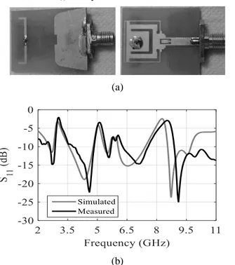
(a)
(b)
Fig. 6. (a) fabricated antenna (b) The comparison between simulated and measured S11 ofpropose four notches antenna
V. RESULTS AND DISCUSSION
(4.73-5.25GHz), (5.54-6.12GHz), and (7.6-9.1GHz). An acceptable matching was observed between simulated and measured results with little difference due to a fabrication error.
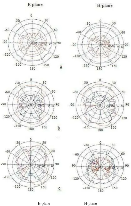
E-plane H-plane
Fig. 7. Radiation pattern at a) 2.6GHz, b) 5GHz, and c) 9.5GHz. (in E-plane red color is Co polarization and blue is Cross-polarization and in H-plane red color is Cross-Cross-polarization and blue color is Co-Cross-polarization)
E-plane pattern is bidirectional in nature. The comparison between simulated and measured gains of the UWB antenna with four notched bands bands is shown in Fig. 8. The average gain of the proposed antenna is nearly constant, 3dBi in the entire UWB range. However, by the introduction of four notch bands at 3, 5.3, 5.8 and 8.4 GHz frequencies, the gain becomes negative which shows the good band-notch performance of UWB antenna.
Fig. 8. Comparison results between simulated and measured gain of proposed antenna
Fig. 9. Radiation efficiency of the proposed antenna
Fig.
9
presents the efficiency of the proposed antenna, which is approximately over9
5%. The efficiency of the antenna decreased consumedly at notch bands as shown here. Also at thenotch
frequencies
, the antenna efficiency reduced to50%
.(24, 25, 26, & 27). The proposed antenna is compared with other 4 UWB antennas regarding three parameters of bandwidth, the number of notches, and overall size.
The characteristics of the mentioned antennas are summarized in Table 1. The Schematic structure of the Analytic Hierarchy Process is explained in 3 parts. The first part is the goal of the study. The other two parts are the substrates of the goal; in these sections, the antennas and the regarding characteristics are discussed. In the present study, comparing the effective factors for selecting an antenna with the capability to remove 4 bands, the researchers could be able to choose the most appropriate antenna.
The schematic structure of the AHP is shown in Fig. 10. Here “Selecting the best antenna structure” is pursued.
AHP is a simple method of comparison which helps avoid the complexity of other methods and make the right choice. For example, the aim of the present study was to design an antenna with a high bandwidth, small size, and high number of notches. Applying this method, one can easily choose the appropriate antenna from among several similar antennas designed previously equation for assessing the aforementioned antennas is introduced here:
(1)
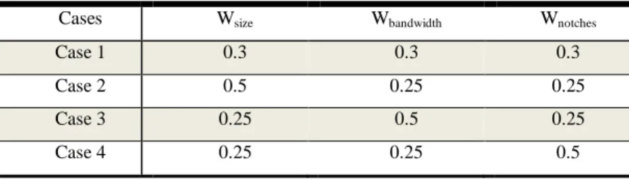
In the above equation, , and are the values given to size, bandwidth, and notch, respectively. The features of the proposed antenna such as size, bandwidth, and the number of notch bands, along with the 4 previously designed antennas are presented in Table 1. Implementing Expert choice software and employing AHP technique for comparing the 4 cases with different values presented in Table 2, one can recognize the superiority of each of the antennas. The comparison is presented in Table 3.
As can be seen from Figure 11, with regard to the first case, all the features had the same weight
value and the proposed antenna was the best choice. In the second case, ‘size’ had the most weight
value, thus the antenna number 25 was the best choice. With regard to the third and fourth cases,
Fig. 10. Analytical Hierarchy Process (AHP) schematic for the antenna selection problem
Table 1. comparison of the proposed antenna size and simulated characteristics with other
references. the impedance bandwidth is for a frequency range where VSWR ≤ 2;
Ref. Size (mm3) BW (GHz)- % Substrate(εr) Notch number
[24] 35×35×1.6 (2.8-11.8)-123.29% (4.4) 3
[25] 21×28×1.6 (2.8-11.3)-120.57% (2.65) 3
[26] 36.6×26.6× 1 (2.5-10.9)-73.68% (4.4) 3
[27] 35×30×1.5 (3.1-10.5)-108.82% (2.65) 3
This work 26×30×1.6 (2.55-11)-124.72% (4.4) 4
Table 2. 4 cases with different values for the various attributes
Cases Wsize Wbandwidth Wnotches
Case 1 0.3 0.3 0.3
Case 2 0.5 0.25 0.25
Case 3 0.25 0.5 0.25
Case 4 0.25 0.25 0.5
Table 3. Utility values of the antennas in four different cases for weight assignments
Cases This antenna Antenna[24] Antenna[25] Antenna[26] Antenna[27]
Case 1 0.225 0.181 0.221 0.191 0.182
Case 2 0.219 0.169 0.232 0.204 0.176
Case 3 0.226 0.193 0.221 0.174 0.186
0 0.05 0.1 0.15 0.2 0.25
Case1 Case2 Case3 Case4
This antenna Antenna[24] Antenna[25]
Antenna[26] Antenna[27]
Fig.11. Utility values for the antennas in four different cases
VII. CONCLUSION
In this study, a new UWB antenna is proposed with dimensions of 26×30×1.6 mm3 and the capability of filtering the disturbing frequency bands of WLAN, a part of C-Band, S-Band, and X-Band (satellite service bands as identified by the International Telecommunication Union (ITU)). This antenna is able to cover the broadband frequency from 2.55 to 11 GHz for VSWR<2. Also, the three main characteristics of this antenna are: 1) Wide bandwidth, 2) proper radiation performance, and 3) small size.
Moreover, a detailed comparison was done using Expert choice software and AHP technique. The results revealed that the proposed antenna is the best choice for the mentioned purpose. This technique provides a convenient and accurate assessment for users to make a right choice when selecting the required antenna for specific applications. The simulated and experimental results confirmed that the proposed antenna could be a good candidate for UWB applications.
ACKNOWLEDGMENT
The authors thank of the Islamic Azad University of Urmia, Iran, for allowing us to use the PNA-X network analyzer system (N5242A) for testing antenna in microwave laboratories.
REFERENCES
[1] Tang, Z.-j., Zhan, J. and Wu, X.-f, "Compact triple band-notched printed antenna with multi slots for UWB applications," Microwave And Optical Technology Letters, Vol. 57, pp. 2056–2060, 2015.
[2] Y. F. Weng, S. W. Cheung and T. I. Yuk, "Design of multiple band-notch using meander lines for compact ultra-wide band antennas," IET Microwaves, Antennas & Propagation, Vol. 6, pp. 908-914, June 7 2012.
[3] A. De Oliveira, M. Perotoni, S. Kofuji and J. Justo, "A Palm Tree Antipodal Vivaldi Antenna With Exponential Slot Edge for Improved Radiation Pattern", IEEE Antennas and Wireless Propagation Letters, vol. 14, pp. 1334-1337, 2015.
[4] Y. Cho, K. Kim, D. Choi, S. Lee and S. Park, "A Miniature UWB Planar Monopole Antenna With 5-GHz Band-Rejection Filter and the Time-Domain Characteristics", IEEE Transactions on Antennas and Propagation, vol. 54, no. 5, pp. 1453-1460, 2006.
[5] K. Shan, C.L. Ruan, and L. Peng, ''Compact UWB antenna with band-notchedcharacteristic using a coupling strip,'' International Symposium on IntelligentSignal Processing and Communication Systems, pp. 1–4, 2010.
[6] P. Gao, L. Xiong, and J.B. Dai, ''Compact printed wide-slot UWB antenna with3.5/5.5 GHz dual band-notched characteristics,'' IEEE Antennas Wireless Propag Lett , Vol12, pp. 983–986, 2013.
[7] N. Mohammadian, M.N. Azarmanesh, and S. Soltani, ''Compact ultrawideband slot antenna fed by coplanar waveguide and microstrip line with triple-band-notchedfrequency function,'' IET Microwave Antennas Propag, Vol 4, pp. 1811–1817, 2010.
[9] R. Zaker, C. Ghobadi, and J. Nourinia, ''Bandwidth enhancement of novel compact single and dual band-notched printed monopole antenna with a pair of L-shapedslots,'' IEEE Trans Antennas Propag, Vol 57, pp. 3978–3983, 2009.
[10]DE OLIVEIRA, Alexandre M. et al. "A palm tree antipodal Vivaldi antenna with exponential slot edge for improved radiation pattern," IEEE Antennas and Wireless Propagation Letters, v. 14, p. 1334-1337, 2015.
[11]S. Mohammadi, J. Nourinia, and C. Ghobadi,'' Compact CPW-fed rotated square-shaped patch slot antenna with band-notched function for UWB applications,'' Electronics Letter, Vol. 47, pp. 1307–1308, 2011.
[12]O. Nasser, O. Mohammad, and G. Noradin, ''Dual band-notched small monopole antenna with novel W-shaped conductor backed-plane and novel T-shaped slotforUWB applications,'' IET Microw. Antennas Propag, Vol. 7, pp. 8–14, 2013.
[13]P Syam Sundar, Sarat K Kotamraju, B T P Madhav, M Sreehari, K Raghavendra Rao, L Prathyusha, Y Pravallika, ''Parasitic Strip Loaded Dual Band Notch Circular Monopole Antenna with Defected Ground Structure,'' International Journal of Electrical and Computer Engineering(IJECE), Vol 6, pp. 1742-1750, 2016.
[14]Y. J. Cho, K. H. Kim, D. H. Choi, S. S. Lee, S. O. Park, A Miniature WB Planar monopole Antenna With 5-GHz Band-Rejection Filter and the Time-Domain Characteristics,'' IEEE Transaction Antennas and Propagation. Vol. 54 No. 5, May 2006.
[15]Ma, T.G., Wu, S.J, ''Ultrawideband band-notched folded strip monopole antenna,''IEEE Trans. Antennas Propag, Volume 55, pp. 2473–2479,September 2007.
[16]Kim, J., Cho, C.S., Lee, J.W, ''5.2 GHz notched ultra-wideband antenna using slottype SRR'', Electron. Lett, Vol 42, No 6, pp. 315–316, March 2006.
[17]Arash Khalilzadeh, Adrian Eng-Choon Tan, Karumudi Rambabu, ''Design of an integrated UWB antenna with dual band notch characteristics,'' International Journal of Electronics and communications, Vol 67, pp. 433-437, 2013. [18]Weng, Y.F., Cheung, S.W., Yuk, T.I, ''Triple band-notched UWB antenna using meandered ground
stub,''Loughborough Antennas and Propagation Conf.,Loughborough, pp. 341-344, November 2010.
[19]Ziyang Wang, Jinhai Liu, Yingzeng Yin, ''Triple Band-Notched UWB Antenna using novel asymmetrical resonators,'' International Journal of Electronics and Communications, Vol 70, 2016.
[20]DS Ramkiran, B T P Madhav, Kankara Narasimha Reddy, Shaik Shabbeer, Priyanshi Jain,Saggurthi Sowmya, ''Coplanar Wave Guide Fed Dual Band Notched MIMO Antenna,'' International Journal of Electrical and Computer Engineering (IJECE), Vol 6, pp. 1732-1741, 2016.
[21]Dong, Y.D., Hong, W., Kuai, Z.Q., Chen, J.X, ''Analysis of planar ultrawidebandantennas with on-ground slot band-notched structures,'' IEEE Trans. AntennasPropag, Vol. 57, pp. 1886–1893, July 2009.
[22]Pancera, E., Modotto, D., Locatelli, A., Pigozzo, F.M., De Angelis, C, ''Noveldesign of UWB antenna with band-notch capability,''European Conf. on WirelessTechnologies, pp. 48–50, December 2007.
[23]Lee, S.H., Baik, J.W., Kim, Y.S, ''A coplanar waveguide fed monopole ultra-wideband antenna having band-notched frequency function by two folded-stripline,'' Microw. Opt. Technol. Lett, Volume 49, pp. 2747–2750, August 2007. [24]Sarkar, D.; Srivastava, K.V.; Saurav, K, "A Compact Microstrip-Fed Triple Band- Notched UWB Monopole
Antenna," Antennas and Wireless Propagation Letters,IEEE, Vol.13, pp.396-399, 2014.
[25]Badamchi, Z. and Zehforoosh, Y. (2015), Switchable single/dual band filtering UWB antenna using parasitic element and T-shaped stub wave cancellers. Microw. Opt. Technol. Lett., 57: 2946–2950.
[26]M. Sefidi, Y. Zehforoosh and S. Moradi, "A small CPW-fed UWB antenna with dual band-notched charectrestics using two stepped impedance resonators", Microwave and Optical Technology Letters, vol. 58, no. 2, pp. 464-467, 2015.
[27]N. Ojaroudi A. Musavand, Y. Zehforoosh and H. Ojaroudi, “A Compact UWB Slot Antenna with Reconfigurable Band-Notched Function for εultimode Applications,” Applied Computational Electromagnetics Society (ACES) Journal, vol. 31, no. 1, pp. 14-18, Jan. 2016.
[28]Sefidi, M., Zehforoosh, Y. and Moradi, S. (2015), A novel CPW-fed antenna with dual band-notched charectrestics for UWB applications. Microw. Opt. Technol. Lett., 57: 2391–2394.