Abstract— Recently research show that some parameters such as the shapes of antenna patch and the ground plane when geometrically altered produces changes in the current density distribution of the planar structure and consequently in the resonant modes. This paper presents a new microstrip fractal antenna using the technique of inserting slots of shape fractal in ground plane in order to increase the bandwidth and insertion discontinuities in the feed line to reach specific behaviors in three resonant modes. The FR-4 substrate with dimensions 85.0 x 85.0 x 1.57 mm³ is used. Also, it used different techniques of impedance matching in feed line of antenna with changes of the width of the transmission line in order to obtain a variation in the current distribution and consequently of the impedance bandwidth for S11
≤ -10dB for C-band (3.625 GHz – 4.2 GHz) and S-band (2.0 GHz – 4.0 GHz). Good agreement between measured and simulated results is achieved. Proposed fractal microstrip antenna can be easily designed, built and applied in wireless communication.
Index Terms— Feed line discontinuity, microstrip fractal antenna, printed slots ground, wireless communication system.
I. INTRODUCTION
Nowadays, the microstrip antennas are especially attractive because of its low cost, low profile and
ease of integration with other circuit elements. The patch and the ground plane may have various
geometric configurations and input impedances are usually 50 Ω or 75 Ω. Some devices in wireless
communications require broadband transmission and even ultra-broadband. In order to obtain the
desired resonant modes is employed the addition of slots in microstrip antenna, both in the patch and
the ground plane [1-3]. The removal of ground plane parts for various applications has been studied,
as curve fractal-shaped for communication systems [4]. Studies of monopole antennas have been
considered in order to find resonant modes for WLAN/WiMAX applications [5]. Investigation of
radiation characteristics for microstrip antennas using geometries such as the island and the curve of
Minkowisk as well as fractal-shaped slots in the ground plane is shown in [6]. Several studies have
shown that the impedance bandwidths for printed antennas can be controlled by coupling between the
patch and the slot in the printed ground plane [7-9]. In [10], the author suggests variation in width of
A New Triple Band Microstrip Fractal
Antenna for C
-
band and S
-
band Applications
Edwin L. Barreto1, Laércio M. Mendonça2,
1
Federal Rural University of the Semi-Arid
Av. Francisco Mota, 572, CEP:59600-97, Mossoró, RN, Brazil 2
Federal University of Rio Grande do Norte, Dept. of Communication Engineering Av. Salgado Filho, 3000 CEP: 59072-970, Natal, RN, Brazil
the antenna's feed line, in order to obtain other resonant modes. Reference [11] shows different levels
fractal geometry can increase the electrical length of the slot sides that help in controlling the resonant
modes and makes the antenna resonates between 2 GHz and 6 GHz. Slots with fractal-shape and the
use of fractals geometry defects in ground plane producing two resonant modes in 2.5 GHz and 5.5
GHz is reported in [12]. Studies of microstrip patch antenna with defected ground structure (DGS) for
WLAN/WiMAX applications are shown in [13].
In this paper, a new triple band antenna fractal microstrip for C-Band and S-Band applications is
proposed. The methodological technique consists initially design and optimize a microstrip patch
antenna with full ground plane fractal with resonate modes at 4.3 GHz and 8.1 GHz. As a second step,
it’s inserted two defects in ground plane and then the microstrip patch fractal antenna adds two resonant modes at 5.0 GHz and 6.8 GHz, besides having controlling of resonant modes and
impedance in the operating range of interest. In this way, the antenna with fractal defect and feed line
discontinuity (¼ wavelength transformer) starts to resonate in three modes: 2.2 GHz, 3.7 GHz and
5.0 GHz for dimensions of specific parameters. The behavior of the resonant modes of the structure
and the influence they suffer due to the level of fractal geometry and defects in the ground plane
structure are important factors to be considered in this paper. Good agreement is obtained between the
simulation and experiment as such as results for resonant modes, far-field E-plane and H-plane
radiation patterns, and gain of the designed antennas. It’s important to note that these resonant modes
include frequency range of communication systems such as WLAN (2.4 GHz / 5.2 GHz / 5.8 GHz)
and WiMax (3.5 GHz / 5.5 GHz). In order to validate the technical proposals is realized a comparison
of the optimized antenna in this paper with another of the literature [13], observing best performance
for the antenna here reported.
The remainder this paper is organized as follows. Section 2 describes the proposed antenna with
resonant modes in terms of the discontinuities of feed microstrip line, patch of antenna and defects in
ground plane. Parametrization analysis is presented and analyzed in Section 3. Section 4 shows the
results and discussion for simulated and measured data are presented and analyzed for the resonant
modes, the linear current density, the radiation patterns and the gain. The conclusion is given in
Section 5.
II. PROPOSED ANTENNA:ANALYSIS AND DESIGN
In this section are analyzed the microstrip fractal antenna techniques and the effects of partial
ground plane removal and of discontinuities of feeding microstrip line on the transmission
characteristics of the proposed antenna. Some tests were performed with various forms of ground
plane and patches in analysis of the antennas and it was choosing the shaped-fractal for these
structures. Fractal geometry offers almost unlimited ways of describing, measuring and predicting the
resonant modes for planar structures of transmission. In computational numerical simulations was
microstrip antennas. After the optimization, the antennas were built and measurements carried out in
UFRN laboratories using an analyzer Vector network of Rohde & Schwarz. The topics following
describe the main parameters in the proposed antenna design.
A. Discontinuities of Feed Line
Figure 1 shows a microstrip feed line with discontinuities, where the line changes the width, being
shown in Fig. 1 (a). The Fig. 1(b) depicts fringing electric field and the Fig. 1(c) shows equivalent
circuit. This change in the width of the microstrip line is widely used for network configuration,
transformers and ¼ wavelength couplers. The main characteristics these lines are: (i) the parasite
effect or fringe fields effect (due to capacitance associated with the widest line of discontinuity);
(ii) the phase-shift related to the discontinuity; (iii) the parasitic effect of a step-junction that is similar
to open-end circuit. These characteristics are parameters used in the analysis of microstrip antenna.
Fig. 1. Characteristics of discontinuities for microstrip line: (a) change in width; (b) appearance of fringe electric field; (c) equivalent electric circuit with two Ls inductances and one Cp capacitance.
B. Patch Antenna
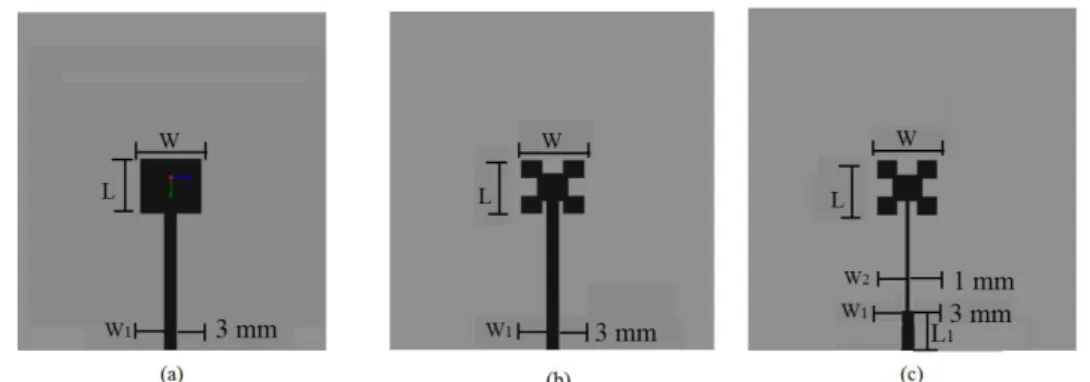
In Fig. 2 are shown three situations of optimized microstrip antennas with full ground planes. For
these designs were used FR-4 substrates with size 85 x 85 mm², relative permittivity 4.4, 1.57 mm of
thickness, and loss tangent = 0.001. Fig. 2(a) shows the patch rectangular shape with dimensions L =
13.34 mm, W = 15 mm. Fig. 2(b) using scale factors for fractal geometry: L/3; L/4; W/3; W/4, for printed patch geometries. In Fig. 2(c) is used the same structure of Fig. 2(b) in order to change the
width of the transmission line. The change in width of the feed line of W1 = 3.0 mm to W2 = 1.0 mm
featuring the discontinuity in the line. The length of the discontinuity W1 corresponds to 1/4 of the
length and width W2, and considering L1= 10 mm.
Figure 3 shows the simulation of the return loss characteristics for the structures shown in Fig
2(a)-(c). In order to do a comparative analysis, we noted that the case with the rectangular patch, it isn't
satisfactory in terms of impedance matching, because it does not reach the insertion loss of -10 dB for
operation of the printed antenna without discontinuities. However, for the case with patch fractal and
using discontinuities results the appearance of resonance modes in 4.3 GHz and 8.1 GHz.
Fig. 3. Return loss for the proposed patch antenna.
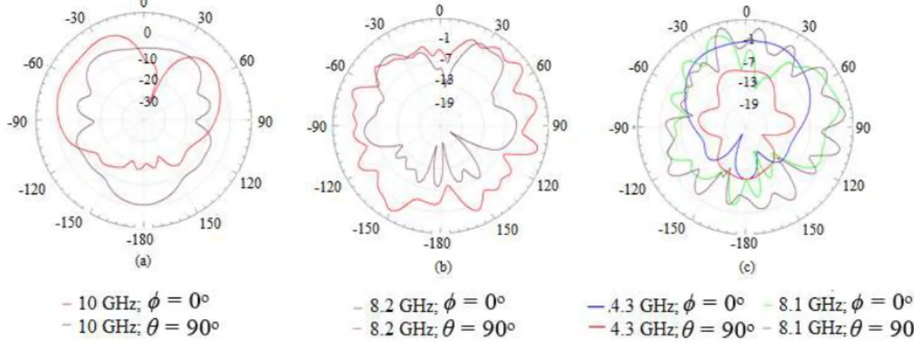
Figure 4 shows the radiation pattern for E-plane and H-plane for the structures of Fig. 2. Fig. 4(a)
depicted the planes ϕ = 0o andθ = 90o with geometry of full ground plane of the rectangular patch
antenna and resonant mode of 10 GHz, whereas for the Fig. 4(b) shows the fractal patch antenna with
resonant mode of 8.2 GHz. Fig. 4(c) shows the patch fractal with discontinuity and resonant modes in
4.3 GHz and 8.1 GHz.
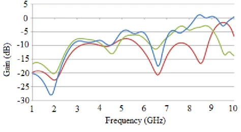
Figure 5 shows the gain of antennas for variations of frequencies between 1 GHz and 10 GHz, and
values less than 0 dBi. This implies in no antenna radiating. Therefore, we have that considering the
insert of defects in the ground plane and realize the analysis on the gain of the antennas.
Fig. 5. Gain simulated for ϕ= 0 ° and θ = 90º considered for cases of geometry with full ground plane. C. Defect on the Ground Plane
The defects on ground plane are used with the optimized patch antenna in order to investigate the
effects of fractal slots in the characterization of printed antennas in search of better behavior. We
tested different shaped-slots on ground plane, as seen in Fig. 6. In Table I is shown the dimensions of
proposed antenna. These values used in the slots are: Lg/3; Wg/3; Lg/4; Wg/4, as seen in Fig.6(c).
TABLE I.OPTIMIZED PROPOSAL ANTENNA
Antenna Dimension Value
W 15mm L 13.34mm W1 3mm
W2 1mm
L1 10mm
Wg 40 mm
Lg 45 mm
Lg/3; Wg/3 15 mm; 13.34 mm
Lg/4; Wg/4 11.25 mm; 10 mm
The fractal antenna seen in Fig. 6(c) was used for the physical construction and measurement.
Figure 7 shows the return loss curves for the case of antennas with ground plane defects (as seen in
Figure 6 (a) - (c)) for the resonant modes in 2.2 GHz, 3.7 GHz, and 5.0 GHz, demonstrating the
operation under triple band. In this case, it was used feed discontinuities in microstrip line and
fractal-shaped slots in the ground plane.
Fig. 7. Return loss for the tested cases of defect ground plane.
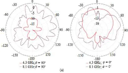
Figure 8 shows the measured radiation patterns in H and E planes of the proposed antenna for the
resonant modes in 4.3 GHz and 8.1 GHz with geometry full ground plane (a), with resonant mode in
6.8 GHz for rectangular-shaped slot on the ground plane (b), and resonant modes in 2.1 GHz, 3.8 GHz
Fig. 8. Radiation patterns of E-Plane and H-plane for cases of defects on ground plane for its resonant modes.
Figure 9 shows the gain peaks in dB in range between 1 GHz and 6 GHz for the proposed antenna.
In this case, fractals elements inserted by Minkowisk curve changed the formation of the fields in
antenna and therefore the insertion of resonant modes for antenna operation to frequencies band of
WLAN and adjusting the gain for a better propagation of the signal.
III. PARAMETRIZATION ANALYSIS
Variations were performed to investigate the relationship of influences on the antenna response as
function of the L1 e W2 parameters. The variation of parameters L1 and W2 have direct influence on
the impedance ratio given by 1/4 wavelength transformer, which causes direct change in the reflection
coefficient and control of frequency. For this test were considered the values of W2 = 0.9 mm; 1.0
mm; 1.1 mm. For L1, were used 7 mm; 9 mm; 10 mm; 11 mm; 13 mm, as shows the Table II. First it
was considered L1 = 10 mm and variations W2 as seen in Fig. 10. After this, it was done simulations
considering W2 fixed in 1.0 mm and variations in L1 as seen in Fig. 11.
TABLE II. PARAMETRIZATION
Fixed Parameter Variety Parameter
L1=10mm
W2 = 1.0 mm
W2=0.9mm
W2=1.0mm
W2=1.1mm L1=7mm
L1=9mm
L1=10mm
L1=11mm
L1=13mm
Figure 10 shows the variation of W2, considering fixed L1 = 10 mm. Thus, it can change the
simulated reflection coefficient and the bandwidth for S11 < -10dB practically unchanged. It happens
for resonant modes in 2.2 GHz, 3.7 GHz and 5.0 GHz.
However, in Fig. 11 are varied L1 and fixed W2 in 1.0 mm. Thus, it is shown a frequency control
up to 500 MHz. Thus, we can make application the control of bands down link and up link for
communication satellites applications.
Fig. 11. Variation L1 Fixed W2 = 1.0 mm
Figure 12 considers different values of W2 and L1 for simulated return loss. It is observed for the
second frequency band a control for the range of 500MHz of bandwidth for the case when W2 = 0.5
mm, L1 = 5 mm. The parametrization shows that changes in the parameters L1 and W2 has effects on
the resonant modes and operation of the microstrip antenna for WLAN application.
IV. RESULTS AND DISCUSSION
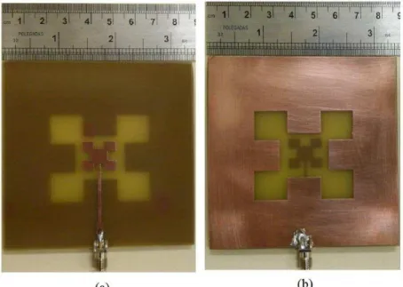
Figure 13 shows the geometry optimized while the Fig. 14 shows a photograph of the fabricated
antenna. For the physical construction and measurement model was used to analysis W2 = 1.0 mm,
and L1 = 7.0 mm. Thus, the results showed que the three bands for reflection coefficient were less
than -10dB, for the bandwidths of the proposed antenna. The numerical values for these three resonant
modes were 2.1 GHz, 3.8 GHz and 5.3 GHz.
Next, we analyze the parameters: (A) return loss, (B) current density distribution, (C) radiation
patterns and gain, and (D) the comparative study between the proposed antenna and the antenna
reported in [13].
Fig. 13. Schematic of the proposed antenna: (a) Patch antenna (b) Ground plane.
Fig. 14. Photograph of the fabricated antenna proposal: (a) microstrip patch; (b) ground plane. A. Return Loss
The behavior three bands have remained, as seen in Fig. 15. Simulations and measurements were
were collected values from the return loss of -10dB. Thus, the bandwidth is for the case with
discontinuity in feed line, bandwidth was BW1 = 75 MHz, BW3 = 250 MHz and BW5 = 350MHz for
measured results and BW2 =203 MHz, BW4 = 840 MHz and BW6 = 100 MHz for simulated results
for frequencies 2.1 GHz; 3.8 GHz; 5.3 GHzrespectively.
Fig. 15. Return loss measured and simulated. B. Current Density Distribution
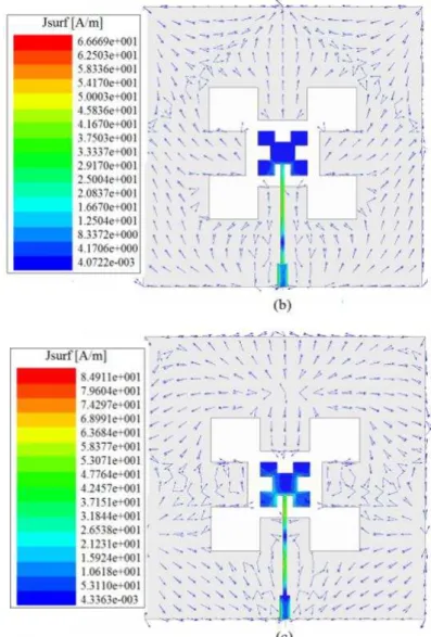
Figure 16 shows the distribution of current density J (A/m) for optimum antenna at frequencies of 2.1,
3.8 and 5.3 GHz. It can be observed that the antenna impedance changes due to the resonant
properties of the discontinuities and ground slot shaped. The surface current concentrated on the edges
of the interior and exterior of the fed by microstrip discontinues. The slits and indentations as well as
the use of discontinuities in microstrip lines is much studied in order to parasitic effects and structures
for linear current distributions analysis. Then observed a radiation pattern similar to a conventional
patch rectangular antenna, in which the maximum radiation in the far field occurs in the direction
Fig. 16. Density current distribution a microstrip line with W1 = 3 mm and W2 = 1 mm: (a); f = 2.1 GHz (b) f = 3.8 GHz; (c)
f = 5.3 GHz. C. Radiations Pattern and Gain
The simulated radiation patterns for the resonant frequencies of the proposal antenna are shown in
Fig. 17. Simulations for far fields E (ZX plane) and H (ZY plane) were obtained using the HFSS
software. Fig. 18 shows gain plot for measured antenna.
Fig. 18. Gain simulated, ϕ = 0 ° and θ = 90º considered. D. Comparative Analysis
Figure 19 shows the comparing the simulation results of the antenna proposed in this work and
results in [13]. It is evident the difference between a dual-band antenna and the antenna in this work
that has three resonant modes operating in 2.1GHz, 3.8 GHz and 5.3 GHz. In this analysis the
simulated bandwidths of proposed antenna were BW1 = 1.912 GHz-2.115 GHz, BW3 = 3.55
GHz-4.39 GHz, BW4 = 5.39 GHz-5.49 GHz; and the gain of 1.4 dBi, 4.8 dBi and 2.9 dBi for 2.1GHz, 3.8
GHz and 5.3 GHz, respectively, while the antenna proposed by Mohammad et. Al [13], presented
BW2 = 2.276 GHz-2.553 GHz and BW5 = 5.144 GHz-5.90 GHz bands with gain 2.053 dBi and 4.52
dBi for resonant modes 2.43 GHz and 5.52 GHz, respectively.
Note that for the two antennas in comparison were used similar techniques such as transformer 1/4
wave, fractal defects and patch geometries.
In table III is shown numerical parameters between the proposed antenna this paper and the
proposed antenna in [13].
TABLE III. SIMULATION RESULTS OF THE ANTENNAS
Parameter Proposed antenna Mohammad et. Al [13]
Resonant Mode Bandwidth Gain
2.10 GHz 3.80 GHz 5.30 GHz BW1 = 203 MHz BW3 = 840 MHz BW4 = 100 MHz
1.4 dBi 4.8 dBi 2.9 dBi
2.43 GHz 5.52 GHz BW2 = 275.5 MHz BW5 = 756 MHz
2.05dBi 4.52dBi
V. CONCLUSIONS
In this paper, we proposed a new tripe band microstrip patch antenna and a technique to increase its
performance. The antenna is designed, optimized and fabricated for S-band (2.0 GHz – 4.0 GHz) and
C-band (3.625 GHz – 4.200 GHz) for weather radar, satellites communications, WLAN and WiMAX
applications. Analyzed results concluded that the proposed antenna operates efficiently for resonant
modes in 2.1GHz, 3.8 GHz and 5.3 GHz. The measured bandwidths of proposed antenna were
75 MHz, 250 MHz and 350 MHz with simulated gain of 1.4 dBi, 4.8 dBi and 2.9 dBi, respectively.
The maximum return loss of −11 dB, −13 dB and −23 dB is obtained for these resonant modes. The enhancement of transmission characteristics, the small size, the light weight and the cost effectiveness
of the proposed antenna makes strong candidature for small and slim wireless devices in
telecommunication systems.
ACKNOWLEDGMENT
The authors thank the Graduate Program in Electrical Engineering and Computer and also the
telecommunication's laboratory of the Federal University of Rio Grande do Norte.
REFERENCES
[1] M.R. da Silva; C.L. Ńbrega; P.H. da Fonseca Silva; A.G D'Assunç̃o,“A new configuration of planar monopole quasi-fractal antenna for wireless communications,” in Electromagnetic Field Computation (CEFC), 14th Biennial IEEE Conference on , vol., no., pp.1-1, 9-12 May 2010.
[2] D.D. Krishna; M. Gopikrishna; C.K. Aanandan; P. Mohanan; K. Vasudevan, “Compact wideband Koch fractal printed slot antenna”, Microwaves, Antennas & Propagation, IET , vol.3, no.5, pp.782,789, August 2009.
[3] K. Cheng-Hsueh; Meng-Ju Chiang; Jia-Yi Sze, “Miniaturized Planar Annular Slot Antenna Design Utilizing Shorting Conducting Strip”, in Antennas and Wireless Propagation Letters, IEEE , vol.8, no., pp.1360-1363, 2009.
[4] M.K. Taher al-nuaimi, “Design of new miniaturized fractal microstrip line fed printed slot antenna”, Internet Communications (BCFIC Riga), 2011 Baltic Congress on Future, vol., no., pp.148, 152, 16-18 Feb. 2011.
[5] Ya Wei Shi, Ling Xiong, and Meng Gang Chen, “Compact Triple-Band Monopole Antenna for WLAN/WiMAX-Band USB Dongle Applications”, ETRI Journal, vol. 37, no. 1, Feb. 2015, pp. 21-25.
[6] S. Verma; P. Kumar, "Printed Multiband Minkowisk Fractal Curved Antenna," in Communications (NCC), 2014 Twentieth National Conference on , vol., no., pp.1-5, Feb. 28 2014-March 2 2014.
[7] Kahrizi, Masoud, Tapan K. Sarkar, and Zoran A. Maricevic. "Analysis of a wide radiating slot in the ground plane of a microstrip line." Microwave Theory and Techniques, IEEE Transactions on 41.1 (1993): 29-37.
[8] Yoshimura, Yoshikazu."A Microstripline Slot Antenna (Short Papers)," in IEEE Transactions on Microwave Theory and Techniques, vol. 20, no. 11, pp. 760-762, Nov 1972.
[10] S. C. Basaran; K. Sertel. "Compact and Planar Monopole Antenna for WLAN and WiMAX Applications." Applied Computational Electromagnetics Society Journal 30.5 2015.
[11]Al-Nuaimi, Mustafa K. Taher. "Design of new miniaturized fractal microstrip line fed printed slot antenna." Internet Communications (BCFIC Riga), 2011 Baltic Congress on Future. IEEE, 2011.
[12]Chen, Wen-Ling, Guang-Ming Wang, and Chen-Xin Zhang. "Bandwidth enhancement of a microstrip-line-fed printed wide-slot antenna with a fractal-shaped slot." Antennas and Propagation, IEEE Transactions on 57.7 (2009): 2176-2179.