Abstract— This paper presents a review with the state-of-the-art of
wireless microsystems for biomedical applications. Aspects including the radio-frequency systems, data acquisition, application specificities (especially those in the context of implantable devices), power consumption and issues associated to their integration are presented. A review of COTS (Commercial Off-The-Shelf) systems and new concepts and technologies are also presented.
Index Terms—Biomedical applications, data acquisition, data transmission,
wireless microsystems, wireless instrumentation.
I. INTRODUCTION
Invasive and implantable biomedical devices for doing diagnostics and for therapy purposes can be
expected in applications ranging from neural [1] up to endoscopic capsule systems with video
transmission [2]. The potential of these systems to open significant business activities in the near
future is high due to the new emerging innovative technologies. The success of such systems can be
explained in part with the advent of microtechnologies, which allowed the miniaturization of sensors
and actuators followed by their integration with readout and communication electronics. Wireless
implantable Microsystems constitute a breakthrough in the way the internal pathologies can be
treated. This means that the radio-frequency (RF) chips can play an important role. In this context,
this review starts with the discussion of issues associated with wireless instrumentation targeted for
biomedical applications. This review also presents the technological aspects related to such devices,
and finishes by presenting future directions of technology and applications.
II. TECHNOLOGY FOR WIRELESS SYSTEMS
A. Operational issues
The Figure 1 shows the currently available frequencies and bands for the several technologies used
in wireless communications. The suitable frequencies for possible use (but not restricted to these
ones) in wireless instruments are those belonged to the so called ISM band (Industrial, Scientific and
Medical), due to its unregulated usage. These frequencies can be freely used without being subjected
to standardization, but keeping the emission powers below the maximum levels imposed by
regulations. This usage-flexibility leaded to the widespread of new applications as further discussed.
Wireless microsystems
for biomedical applications
João Paulo Carmo, José Higino Correia,
Wireless communication technologies
Free usage bands
LR-WPAN 802.15.4 nanoNET
Standardized
DECT
Bluetooth
ZigBee
WLAN 802.11
ISM bands
433.05-434.379 MHz 868-870 MHz 1.88-1.9 GHz 2.4-2.4835 GHz 5.725-5.875 GHz
Radio-frequency (RF) Ultrasonic Magnetic field/ electromagnetic
RFID
Standardized LASER
Optical
IrDA Standardized
Infrared
Figure 1: Currently available frequencies for wireless applications [3]. This figure was reproduced with authorization of the editor (Elsevier Science).
The selection of a frequency for an implantable device is easy but not trivial to do. First, the sizes of
these devices must be the minimum as possible. In this context and as it is of general knowledge, the
antenna is one of the most critical subsystems in wireless communications. This means that the
antenna must be small enough to comply with the size constraints of the microsystems to not
compromise the desired miniaturization. The size reduction can be a problem because the antenna
must be designed for transferring the highest possible power into the receiver.
In the context of implantable devices, the size shortening of antennas can introduce additional
problems of the impedance matching [4]. Additional issues include the biocompatibility and the
bandwidth broadening for avoiding secondary effects related to frequency shifts. However, the
environmental issue (and the most forgotten one) that limits the performance of an antenna (either
transmitting or receiving antenna) is operating inside a lossy and relatively uncharacterized medium.
This means that contrary to what happens within the air, the medium constituted by the human tissue
will dominate the radiation performance of the whole RF link [5]. The antennas can be integrated with
RF chips using either the on-package [6], or the on-chip [7,8] or even the on-wafer [9] technique. The
Figure 2 illustrates for few cases, the respective concept behind the integration technique. The
photographs in the Figure 2(a) belong to a RF transceiver IC, which was fabricated using the
silicon-based (Si-based) System-in-Package (SiP) technology [6]. The SIP technology was invented
by Philips Corporation, on which the microdevices are flip-chip mounted onto passive component
substrates, whose consequence is the footprint area minimization as well as the parasitic elements. A
lateral cut photograph is showed in order to better illustrate this integration concept [6]. To resume, in
the on-package integration the antenna is coupled into the package where the RF chip is supported
(a)
(b)
(c)
Figure 2: Techniques for integrating antennas/heterogeneous technologies into microdevices: (a) on-package [6], (b) on-chip [7,8] and (c) on-wafer [9]. These figures were reproduced with authorization of the editor (Elsevier Science).
The on-chip integration requires more than one integration process for more than one technology,
which can lead to a situation where the technology for fabricating the RF chip can be incompatible
with the one used for fabricating the antenna. The Photographs in the Figure 2(b) shows microsystems
where the antennas were directly fabricated within the microdevice [7,8]. This second technique
presents more advantages when compared with the on-package: both the microdevice and antenna are
simultaneously subjected to the same process steps during the fabrication because they share the same
set of technological rules followed by the microelectronic foundries. This make easy to overcome
impedance mismatching problems and at the same time results on cheaper solutions because no
additional step processes and external connections (on PCBs) are not required. Moreover, it is
possible to obtain more compact and smaller devices than with other techniques. However, the main
drawback of this technique is not allowing antennas whose sizes are far outside of the order of
magnitude of microdevices. Moreover, a new antenna (either with a new shape or new specifications)
implies the project redraw and a new submission to the foundry for fabricating the new microdevice.
Finally, the technique that seems to be promising is the on-wafer because wafer-level-packaging
(WLP) techniques for joining heterogeneous technologies are offered by the industry with a relatively
low-price. The Figure 2(c) helps to understand the WLP technique, e.g., the picture on left is a process
flow to fabricate an antenna for operation in the millimeter-wave range [9]. In this picture, it is easy to
identify few microsystem (microfabrication) techniques: (a) starting with the coplanar waveguide fed
to join the antenna into the substrate (containing the microelectronics); (c) substrate thinning step; (d)
glass dicing. The photograph on left part of the Figure 2(c) shows few prototypes of fabricated
antennas suspended in the cavity of the packaging [9]. This last technique is especially suitable for
integrating patch-antennas (due to their planar shape) with RF chips [10]. A variety of antennas with a
variety of shapes and physical placement are related in the literature, as it is the work done by
Soontornpipit et al [11] who fabricated implantable patch antennas with spiral and serpentine shapes.
The folded shorted-patch antenna in the Figure 3(a) was fabricated by Mendes [12] and it exploits the
third dimension for fabricating small antennas with relatively good radiation characteristics. As
illustrated in the Figure 3(b), specific microfabrication techniques were employed on its fabrication:
e.g., sputtering of top and bottom layers of thin-films made of aluminium (Al) [13], patterning of the
Al top layer [14], adhesive bonding (using the BCB - Benzo Cyclo Butene - as adhesive material [15]),
seesaw cut dicing [16], vias formation by laser ablation, and singulation by dicing [17].
(a) (b)
Figure 3: For the folded shorted-patch antenna fabricated by Mendes[12]: Schematics showing (a) the concept, and (b) the fabrication sequence using microfabrication techniques (by laser ablated vias, sputtering, and so on). These figures were reproduced with authorization of the editor (Elsevier Science).
Finally, the research group of Chow et al [18] explores an outstanding methodology that makes
profit of cardiovascular stents to receive RF signals inside the human body. The precise modelling of the propagation channel inside the human body in conjunction with the equation of skin-depth, [m],
gives a rough estimative of the radiowaves penetration. The averaged parameters help to obtain the
skin-depth and the path-loss characteristics of the propagation medium. However, the simple
consideration of path-loss is not simpler because as stated by Scanlon et al [19], the electrical parameters of the surrounding tissue around the RF receiver and the body’s structure have a strong influence in the radiation pattern of the receiving antenna. The main consequences of this are
difficulties due to fading caused by radiation pattern fragmentation especially observed in the
azimuthal plane. This happen because the human body is composed by a variety of tissues comprising
the skin, fat, muscle, bone, nerve, among others. Therefore, it is required to do an averaging of the
muscle, indicating that this is the dominating type of tissue in an average and healthy human subject [20]. It is a difficult task to obtain both the electric conductivity, [S.m-1
], and the dielectric
constant, r, as the needed parameters for calculating the actual path-loss. Nevertheless and
independently of the electrical parameters that are used, the following skin-depth equation can be used
for obtaining an estimative of the expected path-loss [21]:
1 2 0 0 9 1 ) 18 ( 1 2 10 2 r GHz r GHz f f (1)
where 0=10
-9/(36) F.m-1
and 0=410 -7
H.m-1, are the electric permittivity and the magnetic permeability for the free-space (note that (00)
-1/2
=c), respectively. The quantity fGHz is the RF
frequency expressed in giga-cycles per second. To have an idea of how such difficult is to get the parameters, the cortical bone can present an electrical conductivity, , of 0.1032 S.m-1
and a dielectric
constant, r, of 13.77 [20]. Additionally, in [22] these values are found to be {r=5.2, =0.11 S.m
-1
}, {r=57, =1.12 S.m-1}, and {r=15, =0.26 S.m-1} for bone, for muscle and for fat, respectively. The
difficulty is even more evident when looking these parameters varying with the frequency, as described in [20] where a disparity of values are presented: {r=53, =1.10 S.m
-1
} and {r=51.6, =1.56 S.m
-1
} for 418 MHz and 916.5 MHz, respectively. This difficulty can also be used
in a positive way, as it happened with the work done by Karacolak et al [23] for continously
measuring the itens of glucose (the variations of the electric parameters are used for measuring the
sugar concentration). The previous parameters were used for obtaining the skin-depth for 433 MHz,
2.4 GHz and 5.7 GHz, whose values were observed to be much equal between them. This means that
for high frequencies, the path-loss can’t be the only criterion to follow. In the studies carried out by
Siwiak [24], the muscle tissue of the human body was modeled as a lossy wire antenna for simulating
its interaction with radiowaves. More precisely, the human body were modeled as a cylinder of saline
water with frequency dependeny electrical parameters. These studies resulted in skin-depths of
approximately 60 mm and 26 mm for 433 MHz and 2.4 GHz, respectively [24]. Additionally and as
demonstrated by Anacleto et al [25], the placement of the antenna within the human tissue, mounting
with electronics and other stuff (for example, electrodes for acquiring biopotential signals) will result
in the shifting of the centre frequency and/or on the broadening of the bandwidth.
B. Measurement and data acquisition systems
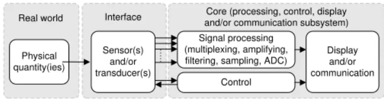
The Figure 4 shows a block diagram of a generic measurement instrument. The blocks of a
measurement system can be grouped into three major types: the real world (representing the physical
quantity to be acquired), the interface block (with the sensor) and the core (e.g., the instrumentation
itself). There are situations where the interface block can be part of the core, e.g., a voltmeter don’t
requires any external sensor because this one is already embedded inside the measuring instrument,
thus the sensing tips can touch directly the electrical potentials. In this context, it must be clarified that
former but if the former is passive (for example, a physical quantity dependant resistor mounted in a
Whitestone bridge) then additional circuits must be provided for obtaining the signal from the sensor.
This means that the set composed by sensor and powering system makes a transducer, confirming that
certain sensors are simultaneously transducers. The core blocks can include electronics of acquisition.
Display and/or communication Signal processing
(multiplexing, amplifying, filtering, sampling, ADC)
Control Sensor(s)
and/or transducer(s)
Core (processing, control, display and/or communication subsystem) Interface
Real world
Physical quantity(ies)
Figure 4: The block diagram of a generic measurement instrument.
The core also provides signal processing functions for signal conditioning purposes. These last
functions include amplification (with the possibility to adjust the gain), filtering (either low pass or
band pass or even high pass filtering) and analog to digital conversion. Then, the user can read the
acquired values in a dedicated display. A more sophisticated core system can interface with the
external world either to connect several measurement instruments or to send data to a central unit for
further processing. These communications can use wired (I2C [26], RS232 [27]) or wireless buses
(ZigBee [28] or customized solution [29]).
The core blocks of the measurement instruments can be analog or digital. The analog is the less
versatile core because requires the presence of a person to annotate the measurements. This type of
instrument is very limited and very difficult to be adapted to wide disparities of signals to measure.
Furthermore, it is not possible to send wirelessly the physical quantities, unless a specific interface
with an analog modulation scheme is provided. A digital core can be used for connecting transducers
(whose output can provide signals in the analog or in the digital domain). The difference from their
analog counterparts resides on the conversion component used in the final processing stage, e.g., the
sampler and the analog-to-digital (AD) converter (ADC) block. The inclusion of multiplexers enables
the acquisition of multiple channels with a single measurement instrument. This topic will be focus of
discussion in the next section. Then and after the ADC conversion, the acquired measurements can be
presented in a numerical display. These cores can also be built with internal memory for storing the
ADC converted samples for rendering in a more complete displaying system (e.g., a planar screen) or
for remote transmitting through a communication interface. This core also allows for changing and/or for programming the amplifier’s gain, thus allowing itself for adapting to wide variations of physical quantities. Finally and thanks to the latest developments of microelectronics, by making available
transducers with digital outputs (for example, integrated monolithic temperature transducers [30], Hall’s effect magnetometers [31] and accelerometers [32], among others) it is possible to have full-digital and reusable cores. The judicious selection of transducers and cores can be decisive points
for fabricating wireless instruments with low-power, reduced sizes and low-prices. This statement is
especially evident on measurement instruments composed by reusable cores (for controlling and
conditioning circuits [33] (for signal processing).
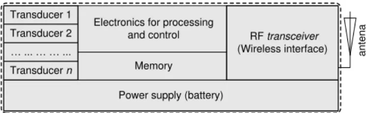
C. RF interfaces
A wireless instrument communicates with the external world by radio-frequency (RF). Thus, a
wireless interface must be provided for allowing RF communications. The Figure 5 shows a generic
schematic block of a wireless microsystem doing functions of a stand-along wireless instrument.
These microsystems are composed by transducers, electronics for control and signal processing, by
memory and by a RF interface (the RF transceiver) for connecting to an associated antenna. The
dimensions of the RF transceiver must be comparable with others elements integrated in the
microsystem (e.g., the transducers and remain electronics). The miniaturization of electronics and the
spreading of fabrication processes for integrating heterogeneous technologies (e.g., CMOS, SiGe,
III/V technologies, MEMS, among others) will result in the mass production of wireless microsystems
at low prices. All these issues combined with the flexibility to select which and the number of
transducers for integrating together with the RF transceiver and remain electronics allows engineers to
design wide number of devices for wide number of applications. This last goal can be easily achieved
with multi-chip-module (MCM) techniques applied to a limited number of components (which can be
of different technologies). In conclusion, the technology is also a major point to allow the fabrication
of wireless microsystems for use in wireless instruments. In this section, few examples for each of the
ISM band in the Figure 1 are presented for a better view of wireless instruments potential.
Power supply (battery)
a
n
te
n
a
Transducer 1
Transducer 2
… ... … … ...
Transducer n
Electronics for processing and control
Memory
RF transceiver
(Wireless interface)
Figure 5: A generic microsystem architecture with an associated antenna.
The Figure 6 shows a photograph of the first prototype (shading area) of a receiver for operation in
the 433 MHz ISM band that was developed for use in implantable Microsystems [34] and was
integrated in a die with an area of 55 mm2. The selected architecture explores the super-regeneration
phenomena to achieve a high sensitivity. This receiver can be supplied with a voltage of only 3 V for
demodulating signals with powers in the range [-100,-40] dB. The combination of modulation and
coding scheme is OOK (on/off keying) modulation combined with a variation of the Manchester code
(a Biphase code). The AMIS 0.7 µm CMOS process was selected for targeting the requirement to
fabricate a low-cost receiver. This receiver is compatible with commercial transmitters, as well as
customized RF solutions such as the transmitter fabricated by Morais et al [35].
Due to its inherent high sensitivity, the new developments around the super-regenerative
architecture are very notorious in the recent years. This is a contradictory point because the
super-regeneration principle was accidentally discovered by Edwin Armstrong in 1922 [36]. The
simplicity of construction and low power consumption [37]. However and despite these positive
points, this architecture was left forgotten during a long period of time due to inherent poor selectivity
and frequency instability [38]. The interest in the super-regenerative receivers stated to grow in the
recent years with a tentative to make such receivers with commercial off-the-shelf components [39],
culminating with a fully on-chip solution fabricated in a 0.8 m BiCMOS process [40]. This last
solution was one of the first successful approaches for obtaining integrated RF chips with receivers
based on the super-regenerative architecture. Since these first steps were done, a wide variety of
circuits were published in the literature for a wide number of applications fabricated with the available
processes. For example, the work conducted by Chen et al [41] resulted in a receiver fabricated in a
0.13 m CMOS process and able to operate at 2.4 GHz with passband tuning. The super-regenerative
receiver fabricated by Moncunill-Geniz et al [42] also operates at 2.4 GHz and was conceived for
high-speed data transfer purposes (e.g., 11 Mbps). Finally, the work proposed by
Moncunill-Geniz et al [43] pushes the super-regenerative concept further by presenting two new
architectures for achieving non-coherent detection of direct-sequence spread spectrum (DSSS)
signals. To finish, it is expected that the potential for use the super-regenerative in modern applications didn’t reached the end-of-line and new developments are expected in the newer future.
Figure 6: A die photography containing the first prototype of a super-regenerative receiver (non-shaded area) [34].
The power consumption of a wireless instrument limits its working time, especially when
functioning with batteries. In this context, the selection (or even further, the design) of RF transceivers can’t neglect this issue because this is the block with major impact in the total power consumption, when compared with the whole electronics in the instrument [44]. Furthermore and
despite the spreading of microelectronics fabrication processes with the potential to achieve smaller
power consumptions, the RF transceiver is irremediably the subsystem of highest power consumption
[45,46]. This demand for the integrated definition of architectures and methods of control, as well as
to provide means to predict the power consumption of the RF system. The Figure 7(a) shows a
photograph of a RF CMOS transceiver at 2.4 GHz for allowing the implementation of control actions,
in a standard 0.18 m CMOS process for achieving low-power consumption with low-voltage supply.
As illustrated in the Figure 7(b), the design of this RF CMOS transceiver predicted the use of control
signal to either select the transmitter or the receiver in order to allow its integration with electronics to
perform custom control. These control signals combined with optimized control protocols can result
in true green networks, where the minimization of power consumptions is a major concern.
An
te
n
n
a
LNA
PA RF switch
Receiver enable
Transmitter enable
External filter
Envelope detector Post-amplifier
Local oscillator PLL @ 2.4 GHz
RXD
TXD Output
buffer
Frequency up-converter
On-chip Frequency down-converter
(a) (b)
Figure 7: (a) Photography and (b) block schematic of a RF CMOS transceiver at 2.4 GHz [47].
It is possible to explore the band located between the 5.7 GHz and the 5.89 GHz for implementing
wireless instruments [48]. This band allows the fabrication of antennas, whose small dimensions
potentiates their integration with electronics using Wafer-Level-Packaging (WLP) techniques. The
integration of antennas and electronics in the same microsystem results in smaller impedance
mismatching problems. Moreover, the antenna and electronics co-integration systematizes the
fabrication process and at the same time results in microsystems with a small cost per unity. The
Figure 8(a) shows a photograph of the wireless interface measuring of 1.51.5 mm2 [49]. The
schematic illustrated in the Figure 8(b) shows the block diagram of the RF part at 5.7 GHz. The
digital signals {S0, S1, S2, S3} select the target frequency in the range
fout=fref(400+2S)=fref[400+2(S0+2S1+4S2+8S3)], whose range is located between 5.42 GHz and
5.83 GHz for a reference frequency fref=13.56 MHz.
An integrated low-cost solution for wireless instruments based on a microdevice fabricated with the
0.18 µm CMOS low-power consumption process can also be found in [50]. This microdevice is
naturally composed by a RF transceiver, by a RISC (Reduced Instruction Set Computer)
microcontroller, by RAM (Random Access Memory) memory, by a power-supply management
circuit, by analog electronics of signal conditioning and analog-to-digital conversion (ADC), and by
circuits for providing communication based in SPI and I2C buses. The control electronics was
developed for implementing a specific communication protocol for use with multiple wireless
instruments and low-power consumption, e.g., the WiseMAC protocol. According the authors, this
protocol working together with their RF transceiver achieves power consumptions thirty times smaller
from 433 MHz and 868 MHz, as well as either with the OOK modulation or the FSK modulation.
According to those claimed, their RF transceiver presents a power consumption of either 2.5 mW or
39 mW, when either the receiver or the transmit operation mode is respectively selected [50].
RF transceiver @ 5.7 GHz
Output driver RF
switch On-chip
External PA
An
te
n
n
a
External base-band down-conversion and
processing circuits RX
TX LNA
PA
Frequency down-converter
Frequency up-converter
Frequency selection
S0S1S3S2
RXD
TXD
Local oscillator PLL @ 5.7 GHz
(a) (b)
Figure 8: (a) A photograph [17] and (b) the respective schematic block of a RF transceiver at 5.7 GHz [49].
III. COTS SOLUTIONS
It is now clear that the biomedical applications are these with the higher potential for using wireless
instruments. An example that confirms this statement is the wireless monitoring systems of human
body information as a growing field. Body area network comprises smart sensors able to
communicate wirelessly to a base station. Examples of applications are the wireless
electroencephalogram (EEG) which is expected that will provide a breakthrough in the monitoring,
diagnostics and treatment of patients with neural diseases. Contrary to the conventional approaches
supported on wires (in the Figure 9(a) is possible to observe such a system for acquiring EEG signals,
where a large number of wires are used to connect the electrodes into the electronics of acquisition
and signal processing), the use of wireless solutions based on wireless modules (composed by the
neural electrodes, processing electronics and a RF transceiver with an associated antenna) will be an
important breakthrough in the way as the EEG diagnostics are made. Two approaches can be used for
implementing wireless EEG systems: the Commercial Off-The-Shelf (COTS) and the customized
solutions. As said by its name, a Commercial Off-The-Shelf solution uses discrete integrated circuits
and passive components for making wireless instruments, whereas a customized solution is designed
from the scratch and further integrated into single microdevices, in order to optimize the size, power
consumption and allow power supply with small batteries (for example, class AA, coin sized
batteries). The system proposed by Dias et al [51] is an example of a COTS system for acquiring EEG
signals and transmission by RF. Basically, this wireless EEG system uses a micaz module from the
Crossbow Company (xbow inc.) [52] at 2.4 GHz for RF transmission and for controlling and
converting the physical data (using the TinyOS operating system). This system uses two class AA
batteries of 1.5 V for power-supply, and achieves the maximum bit rate of 120 kbps. Other features of
this system include the resolution of about 4 V and presents the power consumption is 15 mW and
approximately in 5.7×4.8×2.0 cm3. The Figure 9(b) shows such a wireless system fixed into a human
subject with the help of an elastic band (the white strap) on the thorax region.
(a) (b)
Figure 9: A subject (a) with a conventional EEG system based on wires and (b) with a wireless data acquisiton, logging and transmission system prototype fixed with the help of an elastic band (the white strap) on the thorax region [51].
IV. NEW CONCEPTS
New techniques for implementing wireless instruments can be found in the literature. These
techniques are extremely innovative due to the breakthrough introduced in the way the measurements
are done. The work proposed by Karacolak et al [53] takes in account the variation of the electric
parameters for continuously measuring the items of glucose (the electric parameters varies with the
sugar concentrations). Alternatively, the research group of Chow et al [54] explores an uncommon
(but still very innovative) methodology that makes profit of cardiovascular stents to receive RF
signals inside the human body. In this work, the stents are used as radiating structures for transmitting
the measurements across the tissues of the human body.
The work proposed by Rodrigues et al [55] uses a MEMS antenna with an U-cantilever shaped
structure. Basically, this cantilever is sensitive to the magnetic field component of electromagnetic
waves and will oscillate. A piezoelectric material layer of polyvinylidene fluoride (PVDF) [56] is
used to convert the magnetic field into a voltage useful enough to be understood by the reading
circuit made by Lameiro et al [57]. The major innovation of this technique is allowing the integration
of antennas with implantable devices by way of Wafer-Level-Packaging (WLP) techniques for
achieving the fabrication of small sized devices. Their antenna occupies an area of 1.51.5 mm2 [55].
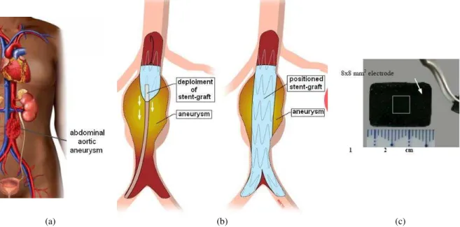
Another outstanding application is proposed by Sepulveda et al [58], where a capacitive sensor
made with a polymer can be used to measure the blood pressure on patients that were recently
subjected to an implantation of a stent-graft. The stent-grafts are widely placed within the veins to fix
a specific pathology, e.g., to close cardiac aneurysms. As showed in the Figure 10(a), an aneurysm is
a permanent and irreversible localized dilatation of an artery, having at least a 50% increase in
diameter compared with the common one. As showed in the Figure 10(a), this capacitive sensor found
on [58] closes the aneurism and at the same time provides a mechanism for monitoring the blood
the endovascular aneurysm repair and thus, avoiding the need for an open surgery. The process flow
used to fabricate this type of capacitive sensor [58] are based on an emergent nanotechnology: the
Carbon Nanotubes (CNTs) Science. In the Figure 10(c) is possible to observe a photograph of a
prototype of this capacitive sensor, which present a cavity dimension of 88 mm and a thickness of
0.8 mm [58]. Basically, the capacitive sensor is based on two square-plate electrodes which act as a
diaphragm and is separated by a dielectric (normally made of air) at a given pressure. The working is
very simple but very ingenious: the variations of pressure outside of the diaphragm make the
square-plates to bend, changing the capacitive proportional to the pressure changes.
(a) (b) (c)
Figure 10: (a) Illustration of an aneurysm localized in the aorta. (b) Artwork showing the endovascular aneurysm repair concept, using stent-grafts. (c) Photograph of fabricated sensors [58]: reproduced with authorization of Elsevier Science.
To finish, a new breakthrough can be obtained by doing the co-integration of the electronics with
microbatteries made of thin-film materials to provide energy in a harvested fashion [59]. This
microbattery supplies the microsystem in an enough time to increase the useful life of the
microsystem. The Figure 11 shows an artwork (for better illustration of the concept) [60] and a
cross-section SEM image of the microbattery prototype made of thin-films [61].
Protective coating
(Si3N4)
Cathode current
collector (Ti+Pt) Anode current collector
Cathode (LiCoO2)
[100] silicon substrate
Anode (Li)
Electrolyte (LiPON)
(a) (b)
ACKNOWLEDGMENT
This work was fully supported by the Algoritmi’s Strategic Project UI 319-2011-2012, under the
Portuguese Foundation for Science and Technology grant PEst-C/EEI/UI0319/2011.
REFERENCES
[1] K. T. Lau, et al., “A low-power synapse/neuron cell for artificial neural networks”, Microelectronics Journal, Vol. 30, pp. 1261-1264, 1999.
[2] B. Chi, et al., “Low power high data rate wireless endoscopy transceiver”, Microelectronics Journal, Vol. 38, pp. 1070-1081, 2007.
[3] J. P. Carmo, and J. H. Correia, "Low-power/low-voltage RF microsystems for wireless sensors networks", Microelectronics Journal, Vol. 40, No. 12, pp. 1746-1754, December 2009.
[4] M. D. Weiss, et al., "RF coupling in a 433-MHz biotelemetry system for an artificial hip", IEEE Antennas and Wireless Propagation Letters, Vol. 8, pp. 916-919, 2009.
[5] A. K. Skrivervik, and F, Merli, "On the efficient design, analysis and measurement of bio-compatible electrically small antennas", 2010 URSI International Symposium on Electromagnetic Theory, pp. 853-856, Berlin, Germany, 2010. [6] F. Roozeboom, et al., "Passive and heterogeneous integration towards a Si-based System-in-Package concept”, Thin
Solid Films, Vol. 504, No. 1-2, pp. 391-396, May 2006.
[7] B.-J. Gu, et al., "Wireless smart sensor with small spiral antenna on Si-substrate”, Microelectronics Journal, Vol. 42, No. 9, pp. 1066-1073, September 2011.
[8] M. Fernández-Bolaños, et al., "Dipole antenna and distributed MEMS phase shifter fully integrated in a single wafer process for beam steering applications”, Microelectronic Engineering, Vol. 87, No. 5-8, pp. 1290-1293,
May-August 2010.
[9] E. Herth, et al., "Wafer level packaging compatible with millimeter-wave antenna”, Sensors and Actuators A: Physical, Vol. 173, No. 1, pp. 238-243, January 2012.
[10]A. Polyakov, et al., “High-resistivity polycrystalline silicon as RF substrate in wafer-level packaging”, Electronic Letters: The IET, Vol. 41, No. 2, pp. 100-101, 2005.
[11]P. Soontornpipit, et al., "Design of implantable microstrip antenna for communication with medical implants", IEEE Trans. on Microwave Theory and Techniques, Vol. 52, No. 8, pp. 1944-1951, 2004.
[12]P. M. Mendes, et al., “Integrated chip-size antennas for wireless microsystems: Fabrication and design considerations”, Journal of Sensors and Actuators A: Elsevier Science, Vol. 125, pp. 217-222, 2006.
[13]J. H. Correia, and J. P. Carmo, Introdução às microtecnologias no silício, LIDEL, Lisbon, 2010. (In Portuguese). [14]L. M. Gonçalves, Microssistemas termoeléctricos baseados em teluretos de bismuto e de antimónio, PhD Thesis on
Industrial Electronics Engineering, University of Minho, Guimarães, Portugal, 2008. (In Portuguese).
[15]P. Abele, et al., “Wafer level integration of a 24 GHz differential SiGe-MMIC oscillator with a patch antenna using BCB as a dielectric layer”, 33rd European Microwave Conference Digest, Vol. 1, October 2003, pp. 293-296. [16]A. C. Peixoto , et al., “Invasive neural electrodes structure fabrication based on aluminum wafers”, Micromechanics
Europe 2012 (MME 2012), Ilmenau, Germany, pp. 1-4. Session A-07, 9-12 September 2012.
[17]P. M. Mendes, Microantenas integradas em microssistemas de rádio-frequência para comunicaçoes sem fios, PhD Thesis on Industrial Electronics Engineering, University of Minho, Guimarães, Portugal, 2005. (In Portuguese). [18]E. Y. Chow, et al., "Evaluation of cardiovascular stents as antennas for implantable wireless applications", IEEE
Transactions on Microwave Theory and Techniques, Vol. 57, No. 10, 2009.
[19]W. G. Scanlon, et al., “Radiowave propagation from a tissue-implanted source at 418 MHz and 916.5 MHz”, IEEE Transactions on Biomedical Engineering, Vol. 47, pp. 527-534, 2000.
[20]D. A. Christensen, et al., “Basic Introduction to Bioelectromagnetics”, 2nd Ed, CRC Press, 2009. [21]J. L. Volakis, "Antenna Engineering Handbook", McGraw-Hill 2007.
[22]R. Pethig, “Dielectric properties of body tissues”, Clinical Physics and Physiological Measurement: Institute of Physics (IOP), Vol. 8, No. Supplementary A, pp. 5-12, November 1987.
[23]T. Karacolak, et al., “Design of a dual-band implantable antenna and development of skin mimicking gels for continuous glucose monitoring”, IEEE Transactions on Microwave Theory and Techniques, Vol. 54, No. 4, pp. 1001-1008, April 2008.
[24]K. Siwiak, “Radiowave propagation and antennas for personal communications”, Third Edition, Artech-House, 2007. [25]P. Anacleto, et al., “Multifunction antenna for compact wireless electrophysiological monitoring devices”, 2010 IEEE
International Symposium on Antennas and Propagation and CNC/USN/URSI radio science meeting, Toronto - Ontário, Canada, 11-17 July 2010, pp. 1-4, paper 427.8.
[26]J. H. Correia, et al., “A CMOS optical microspectrometer with light-to-frequency converter, bus interface and
stray-light compensation”, IEEE Trans. Instrum. & Measurement, Vol. 50, No. 6, pp. 1530-1537, 2001.
[27]L. Korba, et al., “Active infrared sensors for mobile robots”, IEEE Trans. Instrumentation & Measurement, Vol. 43, pp. 283-287, 1994.
[28]H. F. López et al., "Towards the design of efficient nonbeacon-enabled ZigBee networks", Computer Networks: Elseviser Science, Vol. 56, No. 11, pp. 2714-2725, July 2012.
[29]J. P. Carmo, et al., "A low-cost wireless sensor network for industrial applications", Wireless Telecommunications Symposium 2009, Praga, Czech Republic, Session D-2, pp. 1-4, 2009.
[31]M. Motz, et al., “A chopped hall sensor with small jitter and programmable «true power-on» function”, IEEE Journal of Solid-State Circuits, Vol. 40, No. 7, pp. 1533-1540, 2005.
[32]J. Chae, et al., “A monolithic three-axis micro-g micromachined silicon capacitive accelerometer”, IEEE Journal of Microelectromechanical Systems, Vol. 14, No. 2, pp- 235-244, 2005.
[33]A. Arnaud, and C. Galup-Montoro, “Fully integrated signal conditioning of an accelerometer for implantable
pacemakers”, Analog Integrated Circuits and Signal Processing, Vol. 49, No. 3, pp. 313-321, 2006.
[34]J. P. Carmo, et al., "433 MHz implantable wireless stimulation of spinal nerves", 17th IEEE International Conference on Electronics Circuits and Systems, ICECS 2010, Athens, Greece, pp. 227-230, 2010.
[35]R. Morais, et al., “A wireless RF CMOS mixed signal interface for soil moisture measurements”, Journal Sensors and Actuators A: Elsevier Science Direct, Vol. 115, pp. 376 384, 2004.
[36]A. Vouilloz, et al., "A low-power CMOS super-regenerative receiver at 1 GHz", IEEE Journal of Solid-State Circuits, pp. 440-451, 2001.
[37]N. Joehl, et al., “A low power 1 GHz super regenerative transceiver with time shared PLL control”, IEEE Journal of Solid-State Circuits, Vol. 36, No. 7, pp. 1025-1031, 2001.
[38]D. M. W. Leenaerts, “Chaotic behavior in super regenerative detectors”, IEEE Transactions on Circuits and Systems I: Fundamental Theory and Applications, Vol. 43, No. 3, pp. 169-176, 1996.
[39]D. L. Ash, “A low-cost super-regenerative SAW stabilized receiver”, IEEE Transaction on Consumer Electronics, Vol. 33, pp. 395-404, 1987.
[40]P. Favre, et al., “A 2 V 600 uA 1 GHz BiCMOS super regenerative receiver for ISM applications”, IEEE Journal of Solid State Circuits, Vol. 33, No. 12, pp. 218- 2196, 1998.
[41]J. Y. Chen, et al., “A Fully Integrated Auto-Calibrated Super-Regenerative Receiver in 0.13 um CMOS”, IEEE Journal of Solid State Circuits, Vol. 42, No. 9, pp. 1976-1985, 2007.
[42]F. X. Moncunill-Geniz, et al., “An 11 Mb/s 2.1 mW synchronous superregenerative receiver at 2.4 GHz”, IEEE Transactions on Microwave Theory and Techniques, Vol. 55, pp. 1355-1362, 2007.
[43]F. X. Moncunill Geniz, et al., “New superregenerative architectures for direct sequence spread spectrum communications”, IEEE Transactions on Circuits and Systems II: Express Briefs, Vol. 52, pp. 415-419, 2005. [44]J. A. Gutierrez, et al., “IEEE 802.15.4: Develping standards for low-power low-cost wireless personal area networks”.
IEEE Network, Vol. 5, No. 15, 12-19, September/October 2001.
[45]C. Enz, et al., “Ultra low-power radio design for wireless sensor networks”, IEEE International Workshop on Radio-Frequency Integration Technology: Integrated Circuits for Wideband Communication and Wireless Sensor Networks, Singapure, 2005.
[46]C. C. Enz, et al., “WiseNET: An ultralow-power wireless sensor network solution”. IEEE Computer, Vol. 37, No. 8, pp. 62-70, 2004.
[47]J. P. Carmo, et al., "A 2.4-GHz CMOS short range wireless-sensor-network interface for automotive applications", IEEE Transactions on Industrial Electronics, Vol. 57, No. 5, pp. 1764-1771, May 2010.
[48]E. H. Callaway Jr., Wireless sensor networks, Architectures and protocols, Chapter 3: The physical layer, CRC Press, 2004.
[49]N. S. Dias, J. P. Carmo, et al., “A low power/low voltage CMOS wireless interface at 5.7 GHz with dry electrodes for
cognitive networks”, IEEE Sensors Journal, Vol. 11, pp. 755-762, March 2011.
[50]A. El Hoiydi, et al., “The ultra low power WiseNET system”. Design, Automation and Test in Europe 2006, Munich, Germany, pp. 1 5, 2006.
[51]N. S. Dias, J. P. Carmo, et al., “Wireless instrumentation system based on dry electrodes for acquiring EEG signals”,
accepted for publication in the Medical Engineering and Physics, pp. 1-10, 2012.
[52]L. A. Rocha, et al.,“A Body Sensor Network for E-Textiles Integration”. Eurosensors XX, Gothenburg, Sweden, 2006 [53]T. Karacolak, et al., “Design of a dual band implantable antenna and development of skin mimicking gels for
continuous glucose monitoring”, IEEE Transactions on Microwave Theory and Techniques, Vol. 54, No. 4, pp. 1001-1008, 2008.
[54]E. Y. Chow, et al., "Evaluation of cardiovascular stents as antennas for implantable wireless applications", IEEE Transactions on Microwave Theory and Techniques, Vol. 57, No. 10, pp. 2523-2532. 2009.
[55]F. J. O. Rodrigues, et al., "Modeling of a neural electrode with MEMS magnetic sensor for telemetry at low frequencies", MicroMechanics Europe (MME 2009), Toulouse, France, pp. D19/1-D194, 2009.
[56]R. Lameiro, et al., "Large Area Microfabrication of Electroactive Polymeric Structures Based on Near-Field Electrospinning", Proceedia Engineering, Vol. 25, pp. 888-891, 2011.
[57]R. Lameiro, F. J. O. Rodrigues, et al., "Small antenna based on a MEMS magnetic field sensor that uses a piezoelectric polymer as translation mechanism”, MicroMechanics Europe 2010 (MME 2010), pp. 116-119, Enschede,
The Netherlands, 26-29 September 2010.
[58]A. T. Sepulveda, et al., “Nanocomposite flexible pressure sensor for biomedical applications”, Procedia Engineering, Vol. 25, pp. 140-143, 2011.
[59]J. P. Carmo, et al., "Thermoelectric generator and solid-state battery for stand-alone microsystems", Journal of Micromechanics and Microengineering: Institute of Physics (IOP) Publishing, Vol. 20, No. 8, pp. 1-8, August 2010. [60]J. F. Ribeiro, J. P. Carmo, et al., "Enhanced solid-state electrolytes made of lithium phosphorous oxynitride films”,
Accepted for publication on Thin Solid Films, 2012.
![Figure 1: Currently available frequencies for wireless applications [3]. This figure was reproduced with authorization of the editor (Elsevier Science)](https://thumb-eu.123doks.com/thumbv2/123dok_br/18887748.424236/2.892.212.682.106.394/currently-available-frequencies-wireless-applications-reproduced-authorization-elsevier.webp)
![Figure 2: Techniques for integrating antennas/heterogeneous technologies into microdevices: (a) on-package [6], (b) on-chip [7,8] and (c) on-wafer [9]](https://thumb-eu.123doks.com/thumbv2/123dok_br/18887748.424236/3.892.105.783.104.558/figure-techniques-integrating-antennas-heterogeneous-technologies-microdevices-package.webp)
![Figure 3: For the folded shorted-patch antenna fabricated by Mendes [12]: Schematics showing (a) the concept, and (b) the fabrication sequence using microfabrication techniques (by laser ablated vias, sputtering, and so on)](https://thumb-eu.123doks.com/thumbv2/123dok_br/18887748.424236/4.892.124.777.455.740/figure-fabricated-schematics-fabrication-sequence-microfabrication-techniques-sputtering.webp)
![Figure 6: A die photography containing the first prototype of a super-regenerative receiver (non-shaded area) [34]](https://thumb-eu.123doks.com/thumbv2/123dok_br/18887748.424236/8.892.282.623.565.823/figure-photography-containing-prototype-super-regenerative-receiver-shaded.webp)
![Figure 9: A subject (a) with a conventional EEG system based on wires and (b) with a wireless data acquisiton, logging and transmission system prototype fixed with the help of an elastic band (the white strap) on the thorax region [51]](https://thumb-eu.123doks.com/thumbv2/123dok_br/18887748.424236/11.892.110.780.160.423/figure-subject-conventional-wireless-acquisiton-logging-transmission-prototype.webp)