Abstract— An L-strip proximity coupled circular microstrip
antenna is proposed. The structure is investigated using circuit
theoretic approach and simulated using IE3D simulation software.
The patch is designed on a thick substrate of thickness of 11 mm for
a design frequency of 3.74 GHz and provides ultra wide band
operation. The numerical results for input impedance, VSWR,
radiation pattern, efficiency and gain are presented. Bandwidth is
found to be dependent on length of horizontal part of L-strip. A
bandwidth of 69.52% is achieved (for VSWR≤2) for y0=0.112λ0 and
h2=0.097λ0. The beam of antenna rotates with operating frequency.
Index Terms—L-strip feed, Tunability, proximity coupled, wideband,
radiation pattern, antenna gain, radiation efficiency, return loss, directivity.
I. INTRODUCTION
Microstrip patch antennas have been attracting the antenna designers because they offer the features
of low profile, light weight, and compatibility with integrated-circuit technology. Recently, patch
antennas have been receiving a great interest in various wireless communication systems since they
can provide advantages over traditional antennas in terms of efficiency and electromagnetic coupling
to the human head. In many applications, the requirements of bandwidth, tunability and physical size
are quite important. Moreover, many efforts have been devoted to bandwidth widening techniques of
microstrip antennas, including short-circuited termination for microstrip-fed slot antennas by
Ching-Lieh Li, Pei-Ying Lin, and Chun-Kai Huang [1], dual slot loading by Amit A. Deshmukh and Girish
Ganga Prasad Pandey1*, Binod Kumar Kanaujia2
1*
Department of Electronics and Communication Engineering, Maharaja Agrasen Institute of Technology, Rohini, Delhi, INDIA-110086, Email: [email protected]
2
Department of Electronics and Communication Engineering, Ambedkar Institute of Technology, Geeta Colony, Delhi, INDIA- 110031, Email: [email protected]
Surendra. K. Gupta3 and A. K. Gautam4
3
Department of Electronics Engineering, Ambedkar Institute of Integrated technology, Shakarpur, Delhi, INDIA, Email: [email protected]
4
Department of Electronics and Communication Engineering, G. B. P. E. C. Pauri Uttarakhand, INDIA, Email:
Analysis and Design of L-strip Proximity
Kumar [2], use of notch by Y. H. Ge, K. P. Esselle, and T. S. Bird [3], U-shaped ground plane by W.
H. Hsu, and K. L. Wong [4]. For thick patch antenna, the coaxial feed is typically used. However, the
probe inductance limits its impedance bandwidth to less than 10%. K.M. Luk, Y.X. Guo and K.F. Lee
[5] used U-slot and L-probe feed, P.S. Hall [6] used probe compensation, C.L. Mak, K.F. Lee, and
K.M. Luk [7] used T-shape probe for feed and T. Huynh and K.F. Lee [8] used L-shape probe to
overcome band limitation problem. Many researchers have used L-shaped microstrip line as a feed
line. M.K. Meshram used L-strip to to achieve a bandwidth of 56.67% [9] in rectangular microstrip
antenna. Zhongbao Wang, Shaojun Fang, and Shiqiang Fu used modifies L-strip to 22% bandwidth
with improved gain of 9 dBi [10].
In this paper, ultra-wideband proximity coupled L-strip fed Circular Microstrip Antenna (CSMA)
has been presented. Using a foam layer of thickness 11 mm as a substrate, an impedance bandwidth of
69.52% and gain of upto 8 dBi has been achieved which is better than earlier reported results by T.
Huynh and K.F. Lee [8]. No optimization was adopted in the design. The antenna is simulated using
IE3D software. The computed results using circuit theoretic approach agree well with simulated data.
The simulation for antenna efficiency, radiation efficiency, radiation pattern, gain and directivity has
also been carried out.
II. THEORETICAL INVESTIGATION
The L-strip proximity coupled circular microstrip antenna is analyzed using circuit theoretic
approach and cavity model. Broad banding is achieved by using thick substrate. But this reduces
coupling between patch and microstrip feed. Various techniques have been used to counter this
problem. The antenna given Y. X. Guo, K. M. Luk and K. F. Lee [11] is taken as reference for
comparison. In the present analysis L-shaped micro-strip feed is used. The proposed structure is
shown in fig. 1. The antenna structure contains a thick substrate of thickness H. An L-shaped strip line
is designed to couple the power to patch electromagnetically. This L-shaped feed is connected to a
standard microstrip feed which in turn is connected to source. The fig. 2 shows equivalent circuit of
proposed antenna. The length of horizontal part of L-strip under patch is kept less than quarter
wavelength because up to λ/4 length of an open circuited stub, the nature of impedance is capacitive.
The capacitance thus introduced is suppressed by the inductance arising from vertical part of L-strip.
Apart from these, a series resistance arises due to finite conductivity of copper used. The expressions
of series resistance (Rs) and series inductance (Ls) as given by R. K. Huffman (1987) [12] are
] 5 . 0 } / ) {( 2235 . 0
)} /(
2 [ln{ 2 . 0
2 2 2
+ +
+ + =
h t w
t w h h
L
s s
s s s
Fig 1. Structure of proposed antenna.
Fig 2. Equivalent circuit of L-strip proximity coupled CSMA.
0 2
(
)
.
/
13
.
4
h
w
t
f
ρ
ρ
R
s=
s+
s (2)Where ws is width and ts is thickness of strip in mm, h2 is height of L-strip, f is operating
frequency in GHz, ρ is specific resistance of the strip ( cm) and ρ0 is specific resistance of copper.
All antenna metallization is taken as perfect except vertical portion. There is a capacitance (Cs1)
arisingdue to vertical electric fields between horizontal part of L-strip and ground plane in series with
above Ls and Rs and is calculated as
) /( 1 2 0
0
1 wy h h
Cs =
ε
rε
s + (3)Where y0 is penetration of L-strip into patch εr is relative dielectric constant and ε0 is dielectric
constant of vacuum. There is a fringing capacitance between open end of L-strip and ground plane
(Cf1), between open end of L-strip and patch (Cf2) and between radiating edge of patch and horizontal
part of L-strip (Cf2). These capacitances are calculated by evaluating extended effective length of L-Rs Ls
Zin
Cp Rp
Lp Cs1
Cf1
Cf2
C1
Cf2
y0
wS
2a
h2
h33
h1
Microstrip feed
CMSA
GND
H
Top view
strip. The expression of extension in the length of an open ended microstrip line is given by T. C.
Edward [13] and is given as
) 8 . 0 / )( 258 . 0 ( ) 264 . 0 / )( 3 . 0 ( 412 . 0 + − + + = h w h w h l s e s e e
ε
ε
(4)Where εe is effective dielectric constant of material buried under the microstrip line and
ground plane. From T. C. Edward [13] the associated fringing capacitance is calculated as
0 /cZ l
Cf = e
ε
reff (5)Where le is extension in length of L-strip feed, c is velocity of light in vacuum, Z0 is
characteristic impedance of feed and εreff is effective dielectric constant. The fringing capacitance
between horizontal part of L-strip and ground plane (Cf1) is calculated by putting h=h1+h2 and the two
capacitances between patch and horizontal part of L-strip (both Cf2) is calculated by putting h=h3.
Fringing capacitance between patch and L-strip is calculated using equations (4) and (5), ignoring
curvature of patch. The capacitance due to vertical electric field between horizontal part of L-strip and
patch is calculated as
3 0 0
1 y w /h
C =
ε
rε
s (6)The equivalent circuit of L-strip fed circular microstrip antenna is shown in fig. 2. The structure
contains a series RLC resonant circuit in series with a parallel RLC resonant circuit. The parallel RLC
circuit is equivalent of circular microstrip antenna. The resonance resistance Rp of patch, antenna
capacitance Cp and inductance Lp are calculated by Stuart A. Long, Liang C. Shen, Mark D. Walton
and Martin R. Allerding [14] and is given as
}]
{
/[
))
(
(
0 22
ka
J
G
y
a
k
J
R
p=
n−
T n (7)} 2
/{ res p T
p Q f R
C =
π
(8)And Lp =Rp /{2
π
fresQT} (9)Where QT is total quality factor, GT is total conductance of patch of radius a incorporating
radiation loss, conduction loss and dielectric loss [15] and fres is resonant frequency of patch [16].
)
/
1
(
)
/
1
(
1
1
p p p total s s inL
j
C
j
R
C
j
L
j
R
Z
ω
ω
ω
ω
+
+
+
+
+
=
(10)where Ctotal is total capacitance arising due to L-strip (i. e. C1, Cs1, Cf1, and Cf2) and is calculated as
) 2 ( ) )( 2 ( 1 1 2 1 1 1 2 1 f s f f s f total C C C C C C C C C + + + + + = (11)
The reflection coefficient of the antenna is given as
0 0 Z Z Z Z in in + − =
Γ (12)
and the VSWR is calculated as
Γ
−
Γ
+
=
1
1
VSWR
(13)III. DESIGN PARAMETERS
The basic design parameters of the proposed antenna are same as taken by Y. X. Guo, K. M. Luk
and K. F. Lee [11] for comparison purpose. The radius of patch (a) is 17 mm, total height (H) of
substrate is 11mm, and dielectric constant is 1.07 (foam layer). The parameters which are new for the
design are - height of microstrip feed (h1= 1.6 mm or 0.02λ0), height of L-strip (h2= 7.8 mm or
0.097λ0) and gap between circular patch and horizontal part of L-strip (h3= 1.6 mm or 0.02λ0). The
width and length of L-strip are 5mm and 9.5 mm (0.097λ0) respectively. The design frequency of the
antenna is 3.74 GHz (λ0= 80.2 mm). A 50 ohms microstrip line on 1.6 mm thick substrate was taken
to feed the power to L-strip (ws= 5 mm).
IV. RESULTS AND DISCUSSIONS
The L-strip proximity coupled microstrip CMSA is analyzed and the results are compared with the
ones obtained by Y. X. Guo, K. M. Luk and K. F. Lee [11]. The variation of input impedance with
frequency for different horizontal length of L-strip of proposed structure is shown in fig. 3. The
capacitive nature of antenna increases with horizontal length of L-strip. The resonance resistance
decreases as open end of L-strip moves towards center of patch. This indicates that open end is
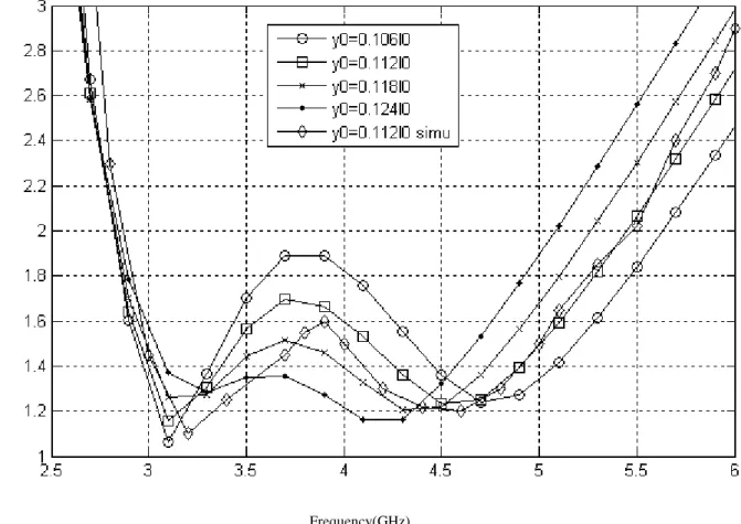
strip is shown in fig. 4. The fig. shows that matching improves with the horizontal length of L-strip.
At the same time, bandwidth decreases due to increased quality factor of the structure. The bandwidth
for different y0 is given in Table I. it is clear that bandwidth decreases with increase in y0 at constant
value of h2. The simulated result is also given in the table which shows a close resemblance with
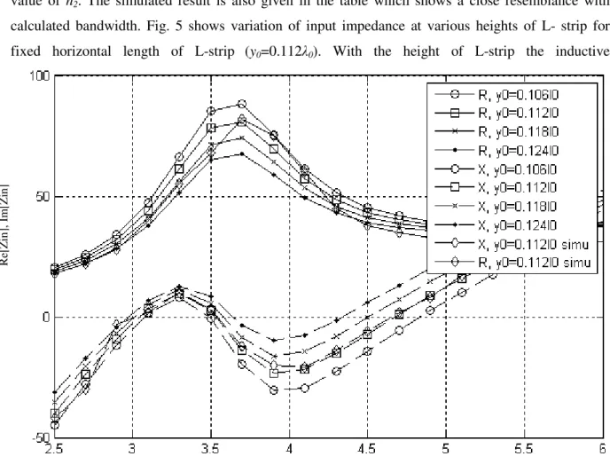
calculated bandwidth. Fig. 5 shows variation of input impedance at various heights of L- strip for
fixed horizontal length of L-strip (y0=0.112λ0). With the height of L-strip the inductive
Frequency(GHz) [R—real part, X---Imaginary part]
Fig 3. Variation of input impedance with frequency for different L-strip lengths h2=0.097λ0.
TABLE I.BANDWIDTH FOR DIFFERENT y0 AT h2=0.097Λ0.
Result y0 fH(GHz) fL(GHz) f(GHz) %BW
C
al
cu
la
te
d
0.106λ0 5.65 2.85 2.8 74.86
0.112λ0 5.45 2.85 2.6 69.50
0.118λ0 5.30 2.85 2.45 65.5
0.124λ0 5.10 2.85 2.25 60.1
Simulated 0.112λ0 5.5 2.90 2.6 69.5
R
e[
Z
in
],
I
m
[Z
in
Frequency(GHz)
Fig 4. Variation of VSWR with frequency for different horizontal length of L-strip at h2=0.097λ0.
Frequency(GHz)
Fig 5. Variation of input impedance with frequency for different height of L-strip at y0=0.112 λ0.
V
S
W
R
R
e[
Z
in
],
I
m
[Z
in
nature increases which is obvious. The variation of VSWR with frequency at different height of
L-strip is shown in fig. 6. The bandwidth for different height of L-L-strip is given in Table II. The
bandwidth decreases with height of L-strip. It is very similar to bandwidth variation with length of
horizontal part of L-strip (y0). Again the simulated and calculated results are in good agreement. The
antenna wassimulated on Zealand IE3D v 14.0 software [17]. The variation of VSWR and input
impedance at y0=0.112λ0 and h2=0.097λ0 are shown in figs. 3, 4, 5 and 6. The calculated results using
circuit theoretic approach and simulated results were in good agreement.
TABLE II.BANDWIDTH FOR DIFFERENT h2 AT y0=0.112λ0.
Result H2 fH(GHz) fL(GHz) f(GHz) %BW
C
al
ul
at
ed 0.091λ0 5.70 2.90 2.80 74.86
0.097λ0 5.47 2.80 2.67 71.39
0.103λ0 4.90 2.70 2.20 58.8
Simulated 0.097λ0 5.25 2.95 2.30 69.52
Frequency(GHz)
Fig 6. Variation of VSWR with frequency for different heights of L-strip y0=0.112 λ0.
V
S
W
The return loss of an antenna shows how well antenna port is matched with source. A good return loss
or VSWR alone is not measure of a good antenna as it does not tell how well the radiation is taking
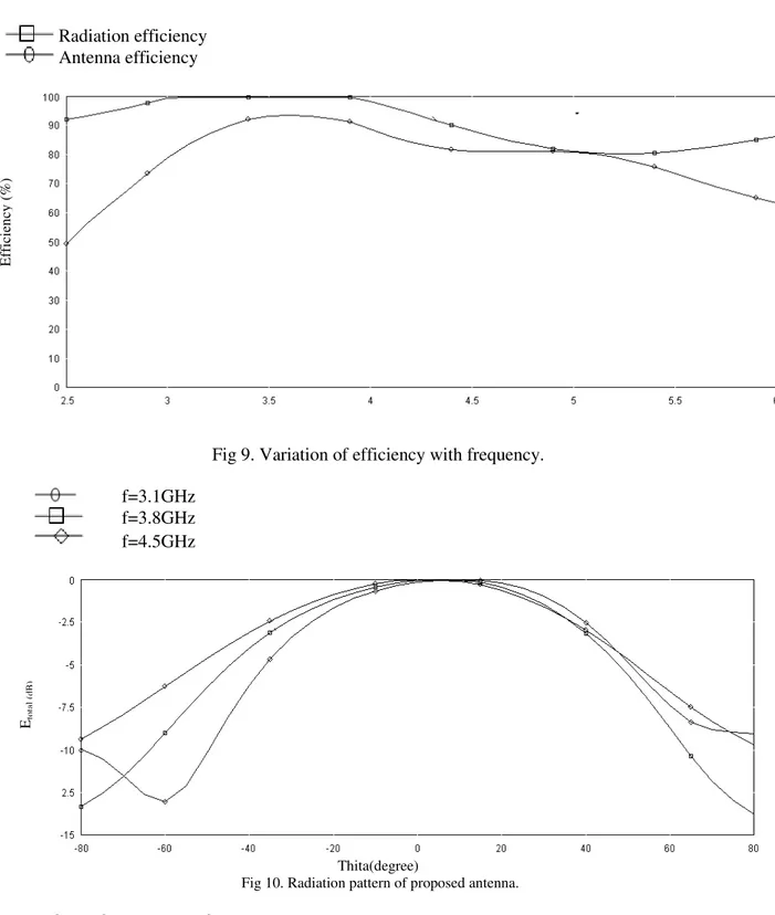
place. Hence investigation of Directivity, radiation efficiency, antenna efficiency and antenna gain is
required. Radiation efficiency of an antenna is defined as ratio of power radiated to power given to
antenna excluding return loss at antenna port. However, the antenna efficiency is defined as ratio of
radiated power to actual power fed to antenna (includes return loss at port). For a good antenna high
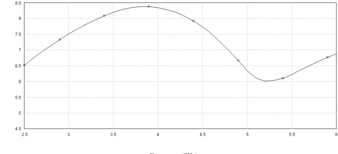
gain, high efficiency is desirable. The variation of directivity at different operating frequency is
shown in fig. 7. It is clear that directivity is maximum (8.4 dBi) at the design frequency and it remains
above 6 dBi for the entire range. The fig. 8 shows variation of maximum antenna gain
Frequency (GHz)
Fig 7. Variation of maximum field directivity with frequency.
Frequency (GHz)
Fig 8. Variation of Gain of the antenna with frequency.
D
ir
ec
ti
v
it
y
(
d
B
)
G
ai
n
(
d
B
with frequency. The gain of the antenna remains more than 4 dBi for the entire range of operation
(2.9-5.5GHz).Total antenna efficiency and radiation efficiency is shown in fig. 9. The antenna
efficiency remains above 80% for the entire range. Total antenna efficiency is above 70%. The
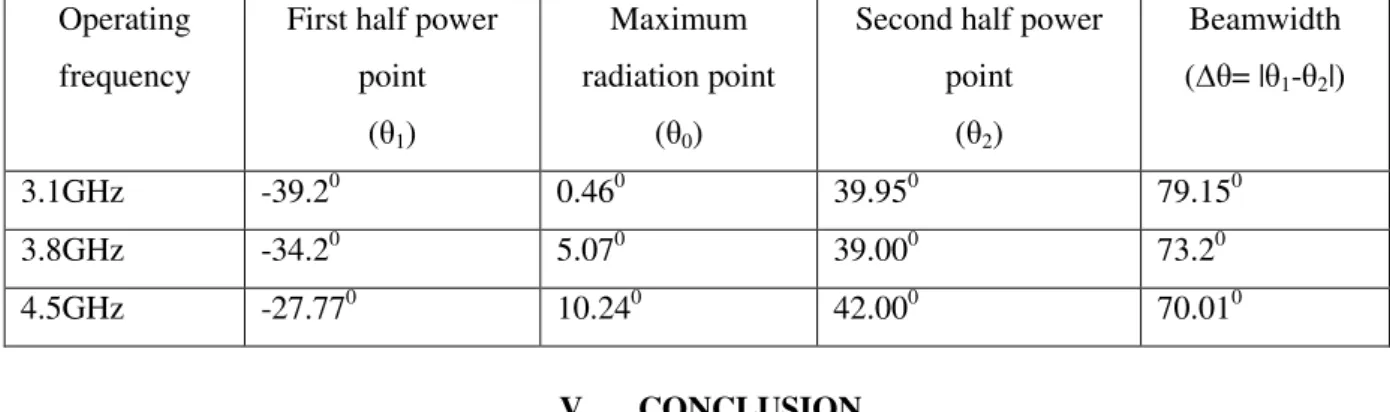
radiation pattern of the proposed antenna using IE3D at 3.1 GHz, 3.8 Ghz and 4.5 GHz is shown in
Fig. 10. It is also observed that beam rotates with frequency of operation. The radiation achieves its
peak
Radiation efficiency Antenna efficiency
Fig 9. Variation of efficiency with frequency.
f=3.1GHz f=3.8GHz
f=4.5GHz
Thita(degree)
Fig 10. Radiation pattern of proposed antenna.
at 0.460, 5.070, and at 10.240 for 3.1GHz, 3.8 GHz and 4.5GHz frequencies respectively. The variation
of beam width and its direction shift is shown in table III. The wave takes definite time to reach at the
E
ff
ic
ie
n
cy
(
%
)
Etot
al
(
dB
feed end and get coupled to the patch. This time delay causes phase difference which in turn affects
the total field in the far field zone. Hence antenna beam rotates for different frequency of operation.
Table III.Beam Rotation at Different Operating Frequency.
Operating
frequency
First half power
point
(θ1)
Maximum
radiation point
(θ0)
Second half power
point
(θ2)
Beamwidth
(∆θ= |θ1-θ2|)
3.1GHz -39.20 0.460 39.950 79.150
3.8GHz -34.20 5.070 39.000 73.20
4.5GHz -27.770 10.240 42.000 70.010
V. CONCLUSION
A novel L-strip fed circular microstrip antenna has been presented for ultra wideband application. An
equivalent circuit was given for the structure and calculations were carried out for circular patch of 11
mm thickness. Various antenna properties were investigated using circuit theoretic approach and
results were verified with simulation. The proposed antenna has an operating frequency range from
2.85GHz to 5.45GHz (2.9GHz to 5.5GHz simulated) and bandwidth of 69.52% which is better than
earlier reported bandwidth (35%) and gain (8 dBi). It may also be concluded that the input impedance
is very sensitive to variation in horizontal length and height of L-strip feed. The beam of antenna is
rotating with the frequency of operation.
REFERENCES
[1] Ching-Lieh Li, Pei-Ying Lin, and Chun-Kai Huang, “Impedance Bandwidth Improvement for Microstrip fed Slot
Antennas Using Short Circuit Termination”, Microwave and optical Tecnology Letters, Vol. 45, No. 1, pp. 67-70,
2005.
[2] Amit A. Deshmukh and Girish Kumar, “Broadband Pairs of Slot Loaded Rectangular Microstrip Antennas”,
Microwave and Optical Technology Letters, Vol. 47, No. 3, pp. 223-226, 2005.
[3] Y. H. Ge, K. P. Esselle, and T. S. Bird, “A Compact E-shaped Patch Antenna with Corrugated Wings,” IEEE
Trans. Antennas and Propagation, vol. 54, no. 8, pp. 2411-2413, Aug. 2006.
[4] W. H. Hsu, and K. L. Wong, “Broad-band Probe-fed Patch Antenna with a U-shaped Ground Plane for
Cross-Polarization Reduction,” IEEE Trans. Antennas and Propagation, vol. 50, no. 3, pp. 352-355, Mar. 2002.
[5] K.M. Luk, Y.X. Guo, and K.F. Lee, “L-probe Proximity Fed U-Slot Patch Antenna,” Electron Lett 34, pp.
1806-1807, 1998.
[6] P.S. Hall, “Probe Compensation in Thick Microstrip Patches,” Electron Lett, 23, pp. 606-607, 1987.
[7] C.L. Mak, K.F. Lee, and K.M. Luk, “Broadband Patch Antenna with a T-shaped Probe,” Proc Inst Elect Eng 147,
pp. 73-76, 2000.
[8] T. Huynh and K.F. Lee, “Single Layer single Patch Wideband Microstrip Antenna,” Electron Lett 31, pp.
[9] M.K. Meshram, “Analysis of L-strip Proximity Fed Rectangular Microstrip Antenna for Mobile Base Station,”
Microwave and Optical Technology Letters, vol. 49, no. 8, pp. 1817-1824, Aug. 2007.
[10] Zhongbao Wang, Shaojun Fang, and Shiqiang Fu, “Wideband Dual-Layer Patch Antenna Fed by a Modified
L-Strip”, Journal of Microwaves, Optoelectronics and Electromagnetic Applications, Vol. 9, No. 2,pp. 89-100, 2010.
[11] Y. X. Guo, K. M. Luk and K. F. Lee, “Regular Circular an Compact Semicircular Patch Antennas with a T-probe
Feeding,” Microwave and Optical Technology Letters, Vol. 31, No. 1, pp. 68-71, 2001.
[12] R. K. Huffman, Handbook of Microwave Integrated circuits, Artech House, Narwood, MA, 1987.
[13] T. C. Edward, Foundation for Microstrip Circuit Design, john Wiley, 1983.
[14] Stuart A. Long, Liang C. Shen, Mark D. Walton and Martin R. Allerding, “Impedance of a Circular Disc Printed
Antenna”, Electronics letters, Vol. 14, No. 21, 1978.
[15] F. Abboud, J. P. Damiano and A. Papiernik, “A New Model for Calculating the Input Impedance of Coax-Fed
Circular Microstrip Antennas with and without Air Gaps”, IEEE Transaction on Antenna and Propagation, Vol.
38, No. 11, pp. 1882-1885, 1990.
[16] Debatosh Guha, “Resonant Frequency of Circular Microstrip Antennas with and without Air Gaps”, IEEE
Transaction on Antenna and Propagation, Vol. 49, No.1, pp. 55-59, 2001.