Abstract — This paper shows fundamentals and results that support a promising methodology for evaluation in locus of a LED from its own radiating signal, and that allows monitoring of its aging by remote inference on which degradation mechanism is acting internally to the device’s structure. It brings out also an alternative route for estimation of parameters of the Shockley’s equation directly from small-signal ac analysis in a simple bench circuit. This last approach is shown to be effective and advantageous relatively to methods which take near a hundred points to achieve good estimations, while it uses only two points of the I-V static characteristic. Both approaches __ referred to as
remote inference method (RIM) and two-pointsmethod (TPM) __ are applied together to show that external quantum efficiency (EQE) can be closely correlated to the injection process assumed to take place in that emitting device, meanwhile overvalued serial resistances due to neutral layers and ohmic contacts in electrodes affect only its electrical performance.
Index Terms— curves I-V,diode, LED, Shockley equation.
I. INTRODUCTION
Static I-V plots use to be analyzed to quality evaluation of diodes or parameterization of their electrical behavior in terms of charge-carrier transport and injection phenomenology, according to the
theoretical model adopted a priori. When real diodes are assumed to follow the Shockley’s formalism __ i.e, their current are due to either diffusion of minority carriers (p-n barrier junction) or thermionic emission of majority carriers (Schottky barrier junction) [1] __ deviations from the ideal exponential
dependence of current on voltage predicted by theory are “saw” by means of an ideality factor (n).
Even for complex last generation LEDs evaluating the n is still a practical use for quality control [2]. Such parameter exhibit values, for example, lying in the range 1<n<2 when a competition between the ideal carrier drift-diffusion process (with n=1) and some generation-recombination process (as the known Sah-Noyce-Shockley’s or Shockley-Read-Hall’s, for which n=2) takes place into the LED [3]. In his paper from late 80’s Werner [4] proposed three approaches to treat I-V data graphically, one of them being cited latter [5]-[8] as a referential methodology for efficient estimation of parameters of
the Shockley equation, when applied for analysis of data from p-n junction and Schottky barrier diodes. For evaluating solar cells and Schottky diodes he applied the well known concepts of
A methodology for performance evaluation of
LEDs based on ac small signal analysis
Isnaldo J. Souza Coêlho, James N. da Silva,
Journal of Microwaves, Optoelectronics and Electromagnetic Applications, Vol. 12, No. 2, December 2013 581
differential resistance and differential conductance all through their curves I-V, and dealt with data directly in relationships (which can be easily demonstrated from Shockley equation [4]) by fitting
selected regions in graphs. Discussions on reliability and precision of estimations for methodologies
like that are surrounded by limitations imposed by internal serial resistance (RS) [6]-[8]. Devices of
special interest like organic LEDs (OLEDs), for example, that have recently increased their
importance in display technology, actually exhibit typical values for RS much higher than their
counterpart crystalline inorganic rivals [9]. That parameter arises in Shockley’s formulation because
injection of carriers, either through p-n or Schottky barriers, both are limited by rates the carriers arrive the junction neighborhood. Therefore, prior to their injection and radiative interaction electrons and holes are transported in the LED’s structure from electrodes towards its optically active junction or layer. Transport layers play a fundamental role not only in light-emission efficiency, but also in the overall device’s electrical performance because they are also responsible for both undesirable effects of additional voltage drops and ohmic power dissipation.
Special attention is paid to RS in many approaches due to the suggested sequences of estimation that
often start by this parameter. The reason is because the knowledge of its value prior to the others
allows the distortion caused by RS in the I-V data to be compensated in the semi-logarithmic scale [4].
In this work a common IR LED (the photo-emitter, PE), available in market elsewhere, is optically
coupled to a photo-detector (PD) whose spectrum matches perfectly to the first. The hypotheses which
justify the key-idea of monitoring internal processes taking place at the PE by means of analysis of the
electrical signals photo-induced in the PD are promptly explained. An innovative methodology for
evaluation of two of the key parameters in the Shockley equation (n and RS) is presented where only a
simple circuit, a two channel oscilloscope and a sinusoidal waveform generator are necessary in the
experimental setup. We start by showing the theoretical fundamentals supporting the method which is
based on small-signal regime operation of the LED. Procedures for characterization of a given LED
are described in detail and algebraic relationships are deduced to be used for estimations from
wave-forms acquired under controlled conditions. Simultaneously the experimental setup is presented for
biasing and excitation of that device as well as for sensing its radiant signal. Then details of the
methodology are described along with the characterization of one sampling device for sake of
exemplification. Estimations for parameters n and RS by means of the referential Werner’s method are
driven from data which were acquired previously and values are compared. Finally, preliminary
results are discussed as well as perspectives and obstacles to be overcome to achieve a better
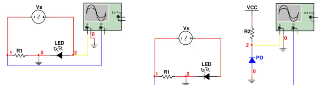
R1
100Ω
A B Ext T rig
+ + _ _ + _ Vs 0 2 1 0 LED
II. THEORETICAL FUNDAMENTS
The Shockley equation (1), which expresses the behavior I-V either for diodes of p-n junction type or Schottky junction type [1], and that can be used also for modeling optoelectronic devices like solar
cells [4] and OLEDs [10]-[11], expresses the main current component as
0 exp 1
nkT i R v e I
i S . (1)
In (1) I0 is the reverse current, RS is the serial resistance (due to ohmic contacts at electrodes and to
non-null resistivity of neutral layers), n is the ideality factor and kT/e ~ 0,026 V at 300 K. The ideality factor n is introduced to fit theoretical curves to experimental data with values greater then unit due to co-existing injection processes taking place together with the main injection process in each kind of
diode [1]. Parameters in (1) are meaningful of what internal charge injection and transportation
processes take place through the structures. So their estimations from analysis of the characteristic
behavior I-V bring fundamental information relatively to those phenomena.
A. Experimental setup
Nothing more than the simple circuits shown in Fig.1a-b are necessary to characterization of the
sampling device under test (DUT). They are composed by one voltage supply (VCC) to bias the PD,
and one ac voltage signal source (Vs), with internally adjustable dc off-set voltage, which is used to
bias and simultaneously to excite the DUT properly. That device should operate under “small-signal”
regime [12] with fixed frequency at a quiescent voltage beyond its forward conductive threshold. Like
described elsewhere when a specific DUT is put to work under such conditions its behavior can be
analyzed according to its equivalent linear model [12], whose parameters are promptly expressed from the dc and ac analyses of the circuit. Figure 1a shows the setup for acquisition of the waveforms arising as result of the electric sinusoidal excitation in the circuit of the PE; while Fig.1b shows how the resulting sinusoidal radiant signal is monitored (i.e, how the optic sinusoidal excitation of the PD is used by means of that circuit to get the information transported by the radiant signal).
Fig. 1 Circuit setup for characterization of LEDs: a) bias and electrical excitation of the sampling DUT; b) bias of the PD optically copled to the sampling DUT (used to monitor its emitted signals).
Proceeding with a typical dc circuit analysis in Fig.1a one easily achieves the expression to estimating the DUT’s threshold voltage:
d
Dos
D
V
r
R
I
V
0
1 , (2)where Vos is the off-set voltage level of the source, rdis the DUT’s dynamic resistance [4,12] and ID is R1
100Ω
A B Ext T rig
Journal of Microwaves, Optoelectronics and Electromagnetic Applications, Vol. 12, No. 2, December 2013 583
the quiescent value of current (bias current or off-set current). On the other hand, ac analysis leads to
b a
d
v
v
R
r
1 , (3)allowing the dynamic resistance to be estimated in the quiescent point directly from readings of signal
waveforms acquired with aid of an oscilloscope (in Chanel A: voltage signal across the DUT, va; in
Chanel B: current signal through the DUT, vb/R1, with dephasing of 180° relatively to the source).
Since the off-set voltage will be defined as a function of the point of quiescent operationQ(ID, VD)
on the I-V curve, according to
D D
os
V
R
I
V
1 , (4)this expression is inserted to (2) together with (3) for allowing one to estimate also VD0 directly from
readings at oscilloscope screen,
B b a A
D v V
v V
V
0 . (5)
In (5), which can obviously be deduced from DUT’s equivalent linear model [12], VA and VB are
the dc voltage levels acquired also by means of channels A and B of that instrument, respectively. Now looking at the circuit in Fig.1b, where the PD is optically coupled to the DUT along with its
electrical characterization as described before, the photo-generated current exhibits both a dc level (IR)
and an ac signal (ir), with the same frequency as the source at the left-hand side circuit (Fig.1a).
B. The Remote Inference Method - RIM
Components IR and ir keep straight correlations with the DUT’s EQE and dynamic resistance (rd),
respectively, since the responsivity of the PD stay stable. Because of the bias current (ID) stability the
level of optical intensity may translate LED’s EQE, meanwhile at the operating point, due to the dependence on rd of the amplitude of its exciting signal (id), the correspondent amplitude of the
optical intensity signal is limited proportionally. In other words, excursions allowed by DUT’s structure to its proper current signal id (see Fig.1a-b) makes its optical emission excursions limited as
well, giving an amplitude to the photo-generated current ir in the PD which depends on rd in the PE.
For a given setup with fixed geometry including the coupled pair PE/PD the ratio between the photo-induced and the exciting currents (R) can be defined such that
r R d D
R
R
I
i
I
i
i
(
)
. (6)Proceeding with the dc and ac analyses of circuits in Fig.1b one achieves, respectively,
B CC
R
V
R
R
R
V
V
1 2
(7a)b
r
v
R
R
R
v
1 2
, (7b)The ratio R could be estimated a priori from (7a or 7b) along with aging of the PE (DUT) giving a “measure” of its EQE, since PD is supposed to maintain its responsivity [13] for a much longer time. However, for engineering application purposes it is the level VR and the signal vr that have to be
monitored along with life-time of LEDs, since (7a) shows an explicit linear dependence on R (i.e, on
EQE of the DUT), while (7b) “brings” also the amplitude of the exciting signal id (i.e, the information
on rd) to the PD by means of vb/R1.
C. The Two Points Method - TPM
When the ac (small-signal) analysis and the Shockley equation are brought together an innovative way to estimate the aimed parameter RSin (1) is revealed. Taking hand of the dynamic conductance
definition (inverse of dynamic resistance [4,12]), an expression arises from (1),
S d
D Q d
d
R
g
nkT
eI
dv
di
r
g
1
1
, (8)showing that RS can be estimated from establishment of an adequate bias point to the DUT,
D d S
eI
nkT
r
R
. (9)Now, combining (9) and (3) and checking the bias current by means of the dc voltage on R1, the
knowledge a priori of the diode’s ideality allows one to estimate RS again from readings at the bench
instrument, taking hand of
b a B Sv
v
eV
nkT
R
R
1 . (10)To conclude the methodology description we suggest n to be estimated by application of (9) in a following step, when the same procedure is run in a second bias point on the LED’s I-V characteristic. From the hypothesis that rd, n and RS are all independent on each other, as well as the last two
parameters are independent on the bias voltage, we get
2 2 1 1 D d D d S
eI
nkT
r
eI
nkT
r
R
, (11)such that
1 2 2 1 2 1 D D d d D DI
I
r
r
kT
I
eI
n
. (12)Here it is worthy to remember the dynamic resistances at both operating points can be expressed
according to (3), while quiescent currents can be measured directly from both dc voltages on each step across R1. Expression (12) can be put into the format
2 1 1 2 1 2 ) ( b a b a B B B B v v v v V V V V kT e
n , (13)
Journal of Microwaves, Optoelectronics and Electromagnetic Applications, Vol. 12, No. 2, December 2013 585
Now it is pointed out that procedures could be quite simplified whether the choice for such a
second bias point was criteriously close to the threshold voltage VD0. Taking hand of (3) again, (13)
could be written as
2 2 2 2
b a B d Dv
v
kT
eV
r
kT
eI
n
, (14)and the ideality factor could be measured directly from circuit in the second bias point at once.
III. PROCEDURES
The kernel of the proposed methodology is to characterize a given LED primarily under its
equivalent linear model for small-signals (available elsewhere [12]), by estimating rd and VD0 always
in the same bias current ID. Such estimations are obtained by means of (3) and (5) directly from
readings at oscilloscope screen. Immediately after the “linear characterization” of that DUT, still
taking hand of direct readings in that same bench instrument, two of the parameters in the nonlinear model expressed by (1) are estimated, n and RS, in this order, by means of (13) and (10). It is
preferable choosing two bias points from which to acquire the waveforms in (13) as suggested before, instead of estimating n by means of (14) from the second bias point only (due to practical reasons to be discussed later). The third parameter (I0) __ whose value could be estimated from plotting the
graph iD vs ln(vD - RSiD) in a following step __ is not included because it is not crucial to the
arguments relative to the aging processes covered by this article.
A. Quiescent operating points and test conditions
An IR LED is now characterized according to the RIM and TPM fundaments. For sake of
verification the efficiency of the proposed methodology is tested by comparing estimations for
parameters n and RS to the values obtained under the Werner’s Plot A method [4]. Its I-V curve is
shown in Fig. 2, considering the cables’ resistance effect (RS, ext = 0.8 ).
Fig.2 – Static I-V curve of the sampling device. The points chosen for bias operation (according to TPM) are shown explicitly, together with the straight line representative of the linear model, the equivalent circuit for operation under small-signal regime around quiescent point Q1.
0,0 0,2 0,4 0,6 0,8 1,0 1,2 1,4 1,6
-10 0 10 20 30 40 50 60 70 80 90 100 110 Q
2(VA2 , ID2 )
Q
1(VA1 , ID1 )
V D0 1/rd2 1/r d1 Q2 Characteristic curve I-V
Data points for Rs,ext = 0R8
F o rw a rd cu rre n t (mA)
Bias voltage (V)
Q
According to that typical I-V curve a bias current ID = 80 mA is established for a dc voltage level
near to VD= 1.4 V. So this is the chosen test current for RIM application purposes, and the first bias
current at which the waveforms in the PE circuit (Fig.1a) are acquired for TPM application purposes.
In circuit of Fig.1a R1 = 100 , so that a dc referential voltage VB = -8.0 V must be verified (by means
of the oscilloscope) as the starting step. The excitation signal from source (vs) is a sinusoidal
wave-form with amplitude 500 mV and frequency 100 Hz, displaced by an off-set of around Vos = 9.4 V
according to what is prescribed in (4).
Plots obtained by handling the original data points in the I-V curve (Fig. 2), for analysis applying the referential methodology [4], are shown in Fig. 3 together with estimations to n, RS and I0.
Fig. 3 – Plotting of data points for estimative of RS from graphical analysis under Werner’s method (plot A [4]).
Inset is part of the compensated I vs (V-RSI) curve from which complementary Shockley’s parameters n and I0 were estimated.
B. Application of new approaches
Typical waveforms from circuit setup are shown in Fig. 4, which are visualized at the oscilloscope
screen for operation around the quiescent point (ID = 80 mA) along with the procedures for
characterization of the DUT under the proposed methodology.
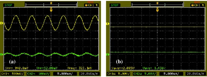
Fig. 4 – Voltage waveforms at points 1 and 2 in circuit setup (see Fig.1a) using a digital oscilloscope (Agilent DSO 3062A): a) signals v1 and v2 are shown with amplitudes 480 mV and 16 mV, respectively; b) dc voltages V1 and V2are shown with levels - 8.01 V
and 1.63 V, respectively. The following correlations relatively to Fig.1a must be highlighted: v1 = vb, v2 = va, V1 = VB, V2 = VA.
0,05 0,10 0,15 0,20 0,25 0,30 0,35 0,40 0,45
0 5 10 15 20 25 30 35 40 45 50
n = 1.38 I0 = 1.7x10 -17 A
R
a
ti
o
g
/I
(V
-1 )
Dynamic conductance (S) Treated data points from curve I-V
Linear fittings
RS = 2.32
1,10 1,12 1,14 1,16 1,18 1,20 1,22 1,24 1,26 1,28 0,001
0,010 0,100
C
u
rr
e
n
t
(m
A
)
Effective voltage (V)
Journal of Microwaves, Optoelectronics and Electromagnetic Applications, Vol. 12, No. 2, December 2013 587
Based on those waveforms and according to (3) one could immediately estimate the dynamic resistance of the DUT at quiescent operation as rd = 3.33 , while the threshold voltage could be
estimated by (5) as VD0 = 1.36 V. For estimating n and RS to equation (1) a second quiescent point is
required, according to the novel methodology, since (13) now can be used to get a value of ideality
which leads to a serial resistance when inserted to (10), together with readings from screen. The waveforms resulting from circuit operation around the lower quiescent current (ID2 = 20 mA) for the
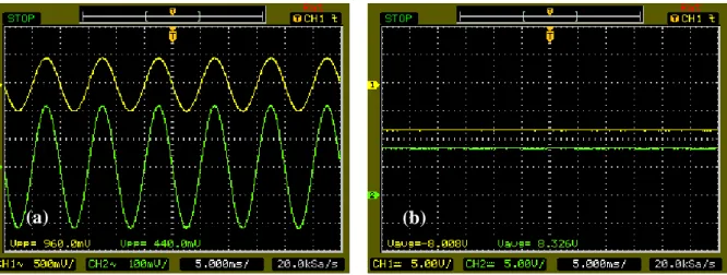
same exciting signal, now displaced by Vos2 = 3.36 V accordingly to (4), are shown in Fig. 5.
Fig. 5 – Voltage waveforms at points 1 and 2 in circuit setup (see Fig.1a) using a digital oscilloscope (Agilent DSO 3062A): a) signals v1 and v2 are shown with amplitudes 470 mV and 26 mV, respectively; b) dc voltages V1 and V2 are shown with levels -2.01 V
and 1.44 V, respectively. The following correlations relatively to Fig.1a must be highlighted: v1 = vb, v2 = va, V1 = VB, V2 = VA.
The Shockley equation (1) possesses a third parameter (I0) whose value will not be estimated,
although it could be obtained from plotting the graph iD vs ln(vD - RSiD) in a following step. However,
it is not crucial to the arguments relative to the supposed aging processes of interest.
According to the waveforms in Fig. 5 the LED’s dynamic resistance increased considerably in the second quiescent point Q2 (see Fig. 2): rd2= 5.53 . Such a higher value is expected due to the greater
proximity to threshold voltage on I-V characteristic. Now tanking hand of (13) an estimation for
ideality is available (n = 2.29) as well as the estimation for serial resistance (RS = 2.60 ) by means
of (10), always keeping in mind the readings at screen of the oscilloscope (Fig.4a-b and Fig.5a-b). Recordings of the trace “2” (Chanel A) in Fig.5a makes it clear, however, how the poor ratio signal/noise in this waveform can affect considerably the precision of estimations. It must be
emphasized that automatic voltage amplitude evaluations the equipment drives by itself are majored,
and some refinement of estimations must be directed (even visually) by the operator.
Turning to the waveforms originated from the coupled circuits and shown in Fig. 6a-b __ which
were obtained simply by taking probe A (i.e, Chanel A of oscilloscope) from point 2 in Fig. 1a to
point 2 in Fig.1b __ the ratio between the photo-induced and the exciting currents (R) can be estimated by means of (7a-b) promptly. The PD’s bias circuit uses a voltage supply VCC= 12 V and a
resistance R2 = 100 k such that R = 4.6x10 -4
. This ratio R must be gauged prior to each test of performance of a given LED, becoming a referential “measure” for evaluating its EQE evolution.
Fig. 6 – Voltage waveforms at points 1 and 2 in coupled circuits (see Fig.1b) using a digital oscilloscope (Agilent DSO 3062A). In this test DUT is biased at ID = 80 mA: a) signals v1 and v2 shown with amplitudes 480 mV and 220 mV, respectively; b) dc voltages V1 and V2 are
shown with levels -8.01 V and 8.33V. The following correlations relatively to Fig.1b must be highlighted: v1 = vb, v2 = vr, V1 = VB, V2 = VR.
C. Simulating increase of RS
When a discrete resistor (RS,ext) is associated externally in series with the DUT, simulating some
degradation process of contacts or transport layers in its internal structure, the TPM is applied again to
get estimations for n and RS, while the RIM’s working is verified. The correspondent voltage signals
and levels measured and used for estimations are shown in Fig.7a-f. Particularly the waveforms in
Fig.7e-f bellow were obtained for RS,ext = 15.8 , keeping the same conditions of excitation of the
DUT’s biasing circuit, as can be confirmed by adding the amplitudes of v1 and v2 in Figs.4a,7a. Note
the re-distribution of voltage signals that got apparent due to the voltage divider performed by R1 and
DUT association in Fig.1a-b. However, due to the resulting increase of “dynamic load” (composed by
this set with two devices) to the exciting source (Vs in Fig.1a), a reduction is expected to take place to
the current signal vb/R1 measured by means of Chanel B of the oscilloscope. The dc voltage across the
DUT, which is measured by means of Chanel A in Fig.1a, is expected to rise since the bias current is
kept the same (ID= 80 mA) in this test. It is clearly shown that both amplitudes were shortened in
Fig.7e, relatively to Fig.6a, meanwhile dc voltage levels measured in Chanel B exhibit almost the same values in Fig. 7f as before (compare with Fig. 6b). It is worthy to emphasize that such behaviors
agree with predictions from (7a-b) for a stable R, since in reality there was not enough time of work to depreciate the internal structure of the LED under test in terms of its level of emission.
Trying to remove effects of noise in the estimations obtained earlier we assumed, according to
Fig.5a, that automatic evaluation for amplitude of signal va is majored by 10 mV (i.e, this is the
average amplitude peak-to-peak supposed for noise). When such an assumption is used to estimating more refined values to the parameters of interest, one achieves n’ = 2.27 and RS’ = 2.08
(associating RS,ext = 0.8 ) and n’’ = 0.49 and RS’’ = 18.29 (associating RS,ext = 15.8 ). For sake of
comparisons both estimations for parameters of the Shockley equation (1) from Werner’s method and
from TPM (with RS,ext = 0.8 and RS,ext = 15.8 ) were inserted to TABLE I bellow.
Journal of Microwaves, Optoelectronics and Electromagnetic Applications, Vol. 12, No. 2, December 2013 589
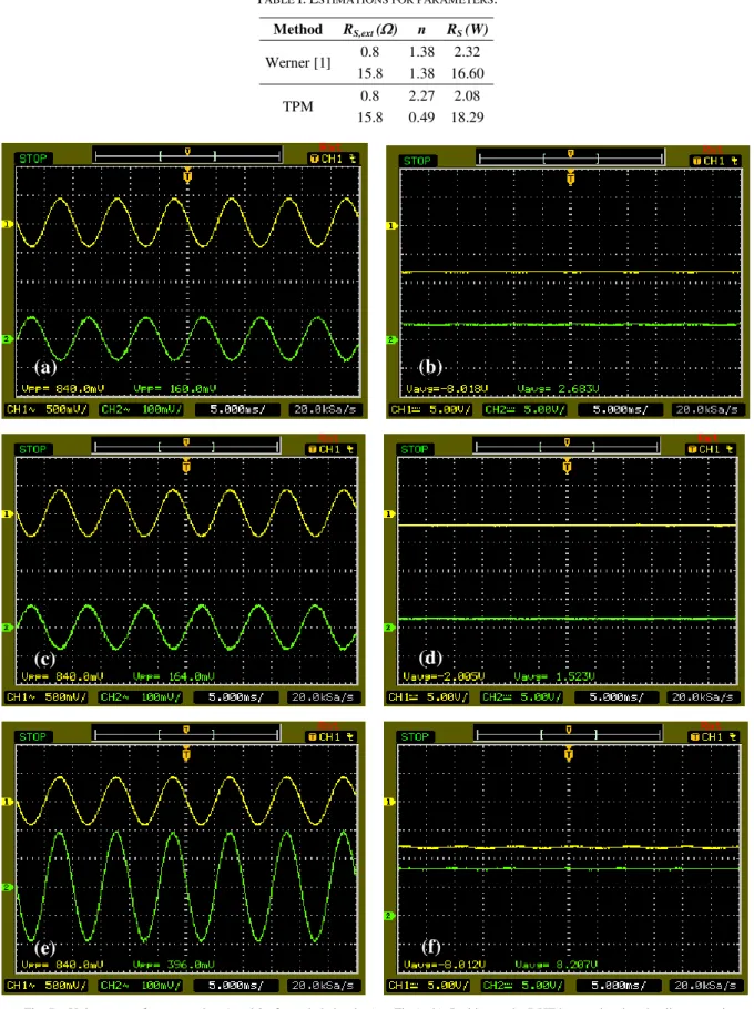
TABLE I.ESTIMATIONS FOR PARAMETERS.
Method RS,ext () n RS (W)
Werner [1] 0.8 1.38 2.32 15.8 1.38 16.60
TPM 0.8 2.27 2.08 15.8 0.49 18.29
Fig. 7 – Voltage waveforms at points 1 and 2 of coupled circuits (see Fig.1a-b). In this test the DUT is associated to the discrete resistor
RS,ext = 15.8 . Proceeding with the TPM: a) bias current at ID = 80 mA; signals v1 and v2 with amplitudes 420 mV and 80 mV, respectively;
b) dc voltages V1 andV2 with levels -8.02 V and 2.68 V; c) bias current at ID = 20 mA; signals v1 and v2 with amplitudes 418 mV and 82.0 mV,
respectively; d) dc voltages V1 and V2 with levels -2.01 V and = 1.52 V, respectively. Relatively to Fig.1a the following correlations must be
noted: v1 = vb, v2 = va, V1 = VB, V2 = VA. Now proceeding with the RIM: e) signals v1 and v2 with amplitudes 420 mV and 198 mV,
respectively; f) dc voltages V1 and V2 with levels -8.01 V and = 8.21 V. Note the correlations in Fig.1b: v1 = vb, v2 = vr, V1 = VB, V2 = VR.
(e)
(f)
(a)
(b)
IV. RESULTS AND DISCUSSIONS
Comparing the estimations obtained to the parameters of interest in the Shockley equation (1)
(recorded in TABLE I) from application of both the Werner’s method and the TPM, the notorious discrepancies appear unacceptable. Such results, however, cannot be attributed to greater efficiency of
one or other methodology in treating the data obtained from I-V curves of a given LED (Fig. 2). Werner’s plot A (Fig. 3) exhibits spreading of experimental points due to limitations (noise) imposed by the instrumentation available in tests. So, linear fittings were obtained only for small sub-sets of
points that align jointly, the reason why they have been selected for linear approximation purposes.
Certainly the estimations are affected by unsatisfactory inclusions or exclusions of significant data
points. It is pointed out, for example, that estimation of I0 seems not to be reliable because of the value
much lower than expected for a real device. Values listed in the first row of TABLE I serve, however, as referential estimations for sake of comparison relatively to the values obtained from TPM.
On the other hand, values listed in the second row (TPM) confirm that proposed methodology is
sensible for estimating n and RS, with earnings in terms of fastness, ease and practicity for tests in
laboratory. Even though those values suffer of inexactness, their estimation took only few minutes of work on bench. It is mandatory to emphasize that “small-signal hypothesis” exact voltage signals with amplitudes smaller than [12] 10% of nkT/e (i.e, smaller than 2.5 mV) otherwise the linear approximation subsidizing the adopted model is severely deniable. To downsize voltage signals,
however, requires additional efforts directed to improvement of the ratio signal/noise (S/N),
something hardly tried at the moment but still not surpassed in our lab. The strength of our theoretical
fundamentation in the TPM’s formulation composes the main argument to uphold its applicability on
quality control of devices, as well as to continue employing efforts on its improvement. Greater
efforts were dedicated for stabilization of waveforms in tests for estimation of ideality factors (n), because the DUT had to be operated closer to its threshold where the dynamic resistances (rd2) are
significantly higher. In the second quiescent point Q2 nonlinear distortion is stronger due to the
“knees” of curves. Efforts would be compensated whether the estimation for n by means of (14) could be satisfactory (according to the waveforms in Fig. 5a, one reaches an alternative value n’’’= 3.9). However, (14) can be deduced directly from (8) or (11) when RS = 0 in that expressions. That is the
reason why estimating n by means of (14) seems not to be the best choice. In fact, the closer is the quiescent point to the “knee” of the LED the smaller is the voltage drop (due to RS) in equation (1).
Contents of TABLE I include also estimations for simulated increase onRS (due to aging processes
related to ohmic contacts or transport layers in the structure of LEDs) by means of inserting an
external resistance RS,ext = 15.8 (this value results from serial association of one resistor of 15 and
the cable’s original resistance), to make clear that TPM is reliable for evaluation of LEDs even for
samples with higher serial resistances. The estimation of ideality becomes difficult, however, when the dynamic resistance gets closer to the serial resistance (now rd = 18.45 W, based on waveforms in
Journal of Microwaves, Optoelectronics and Electromagnetic Applications, Vol. 12, No. 2, December 2013 591
It is worthy to emphasize that even for highly resistive neutral layers the rate of radiative
recombination (i.e, the EQE) can still be made noticeable provided that the bias circuit preserves its capability to sustain the same level of current injected through the structure. In other words it must be
noted that along with its aging a typical LED experiences both increasing of RS and decreasing of
EQE, but not necessarily these effects happen together or directly related to each other. Speaking about OLEDs again, for sake of information, one well known mechanism leading the resistances of
transport layers to rise is the bond-breaking by atmospheric attack, compromising the conjugation in
the polymeric main-chains. Their EQE would not be compromised, however, whether the peripheral ligand molecules were not affected via chemical reaction with oxygen or water [9].
On the other hand, it has to be mentioned the existing discussions on the belief that carrier
injection is governed by another regime in OLEDs, which is known as space-charge limited current
(SCLC) [9], [14]-[15], due to their typically much higher resistive transport layers. Because of the
abrupt change in mobility of electrons when crossing the interface metal-organic semiconductor at
cathode, there would be carriers accumulated imposing further opposition to injection of current in the
structure. In such a point of view the high valued resistance of that neutral layer (said
electron-transport layer [9]) does imply reduction of the EQE of the LED in the sense that it depends on balanced injection of both positive and negative charge-carriers. In that case effects of higher resistive
neutral layers and lower efficiency for radiative recombination are not distinguishable and must be
thought under more careful criteria. Because of the inorganic nature of LEDs treated in this article, the
Shockley Equation is adopted and the alternative formalism based on SCLC is fully discarded. It does
not mean, however, that TPM cannot be applicable for evaluation purposes to OLED’s, since
Shockley formalism is not completely discarded to modeling devices with organic features [10].
Now turning to the tests of performance by remote monitoration via optical signals emitted by the
given LED, it is noticeable the clarity (low noise) of traces in the oscilloscope screen shown if Fig. 6a
and in Fig. 7e, as well as the apparent absence of nonlinear distortion in the transmitted optical signal.
That traces demonstrate the possibility of monitoration of the current signal in the DUT from
photocurrent generated in the PD optically coupled to it, according to (6) and (7a-b). Connecting the
discrete resistor RS,ext = 15.8 an immediate amplitude shortening is noted in the current signal of
excitation (DUT), according to Chanel 1 (compare vb in Fig. 6a to Fig. 7e). This “information” is
transmitted to the PD which receives an optical signal with shorter amplitude, according to Chanel 2.
On the other hand, since the same dc level of current (ID = 80 mA) flows through the DUT (whose
EQE is kept unchanged), the level of photo-current stays stable (compare Fig. 6b to Fig. 7f). These observations open good perspectives for application of the RIM in monitoration of RS and EQE,
because it seems to allow one to identify which mechanism of degradation acts internally to the
In laboratory the ratio R between exciting and photo-induced currents defined in (6) was also measured by means of (7b) after insertion of RS,ext to confirm the stability of the EQE, supposed
earlier from levels VR shown in Figs.6b-7f, according to what is expressed by (7a). Further arguments
could arise from estimations to the parameter VD0 by means of (5) in the linear model approximation,
since mechanisms that lead to increasing rd in the quiescent point are not the same as the mechanisms
that could lead to increasing the threshold voltage along with LED’s lifetime. Equation (9) suggests
that changes of rd could be due to changes either in RS (related to transport phenomena) or in n
(related to injection phenomena) for a given temperature. So, measuring vr could only indicate
whether a change in rd has happened or not, but it does not allow to identify which mechanism is
acting internally to DUT’s structure. Measuring VR simultaneously to vr could, however, allow the
hypothesis of change in n to be discarded for those cases where R was not altered, according to (7a). In such cases VR keeps unchanged and vrexhibits “how” rd behaves (i.e, due to RS only) directly since,
for the same level of charge injection (always ID = 80 mA), the R maintenance points towards the
hypothesis of injection phenomena being preserved. Following the same clue the voltage threshold
estimation (VD0) would arise as some “counter-proof” because it should also exhibit a stable value
along with time. In other words, it is known [1],[16] that positioning of the “knee” of curves I-V is hardly dependent on the ideality n, since this parameter determines how fast the LED’s current “turns on” with voltage in the exponential law (1).
Otherwise when VR changes (probably to a higher value), a behavior that can be attributed only to
changes in R according to (7a), it is certainly due to EQE evolution on time. However, measuring vr
simultaneously to VR could not give conclusive information relatively to RS in the LED because
changes of R imply also changes of amplitude of the transmitted signal. For that cases, it is possible to take hand of (7a) and (7b) to estimate, separately, values to the ratio R allowing to conclude whether
RS has also changed (same R value) or not (differing R values). Such a test makes sense only in
laboratory, being hard to be implemented in circuitry for engineering purposes. Finally, it must be
pointed out the strongly improbable possibility of an increase in VR (i.e, decrease of the EQE) to occur
simultaneously to a decrease in RS (i.e, improvement of contacts and/or conductivity of transport
layers) leading the amplitude of vr to stay the same or to increase with time. Such a behavior is not
expected to happen in generic LEDs along with their life-time.
V. CONCLUSIONS
It is possible to evaluate electrical behavior of LEDs by means of their equivalent linear model for “small-signals” taking hand of the simple circuit setup shown in Fig.1 operated around a specific bias point. The same DUT could be evaluated periodically often times along with its aging, when operated
under identical charge injection conditions. Also, distinct DUTs taken out of the same lot in industry
could be evaluated under standard operating conditions to establish working parameters and for
Journal of Microwaves, Optoelectronics and Electromagnetic Applications, Vol. 12, No. 2, December 2013 593
operational limit of instruments on bench. Maybe the qualification of the new methodology as “state of the art” resides in this fact. Additional efforts searching for reduction of noise must be driven, aiming to improve exactness and precision of estimations to parameters of the Shockley equation.
However, we already demonstrated the potentiality of this methodology for estimation of ideality n
and serial resistance RS in LEDs, with good precision only from two points on its I-V curve. That is an
enormous advantage relatively to other methods, as the Werner’s plot A, which applies many
experimental points for those estimations. Other merits of this new methodology that must be
emphasized are its easy, practicity and fastness for estimative procedures, because it employs
essentially one simple circuit and two common bench instruments. Finally, we also emphasize that the
greater merit of all is to bring with it a possibility of remote monitoration of the performance of a
given LED, supplying meaningful sense of internal processes taking place during degradation of its
structure. In the best of our efforts on researching for anteriority this is a pioneer work.
ACKNOWLEDGMENT
THE AUTHORS ACKNOWLEDGE THE FINANCIAL SUPPORT FROM CNPQ AND FACEPE FOR SCHOLARSHIPS AND GRANTS.
REFERENCES
[1] S. M. Sze, “Physics of semiconductor devices” - Willey, 1981.
[2] J. Bai, Q. Wang, and T. Wang, “Characterization of InGaN-based nanorod light emitting diodes with different indium
compositions” – J. Appl. Phys. 111, 113103 (2012).
[3] C.-T. Sah, R. N. Noyce, and W. Shockley, “Carrier generation and recombination in p-n junctions and p-n junction
characteristics” – Proceeding of the IRE, pp. 1228-1243, September 1957.
[4] J. H. Werner, “Schottky barrier and pn-junction I-V plots –small signal evaluation”, Appl. Phys. A 47, pp.291-300, July
1988.
[5] V. Aubry and F. Meyer, “Schottky diodes with high series resistance: limitations of forward I-Vmethods”, J. Appl.
Phys. 76 (12), pp. 7973-7984, December 1994.
[6] M. Lyakas, R. Zaharia, M. Eizenberg, “Analysis of nonideal Schottky and p-n junction diodes – Extraction of
parameters from I-V plots”, J. Appl. Phys. 78 (9), pp. 5481-5489, November 1995.
[7] A. Kaminski, J. J. Marchand, A. Laugier, “I-V method to extract junction parameters with special emphasis on low
series resistance”, Solid-State Electronics 43, pp. 741-745, November 1998.
[8] A. I. Prokopyev, S. A. Mesheryakov, “Restrictions of forward I-V methods for determination of Schottky diode
parameters” – Measurement 33 (2003), pp. 135-144.
[9] A. B. Walker, A. Kambili, S. J. Martin, “Electrical transport modeling in organic electroluminescent devices” – J. Phys. Condens. Matter 14 (2002), pp. 9825-9876.
[10]M. E. Aydin, F. Yakuphanoglu, J.-H. Eom, D.-H. Hwang, “Electrical characterization of Al/MEH-PPV/p-Si Schottky diode by current-voltage and capacitance-voltage methods” – Phys. B 387 (2007), pp. 239-244.
[11]S. Karg, M. Meier, W. Riess, “Light-emitting diodes based on poly-p-phenylene-vinylene: I. Charge-carrier injection
and transport” – J. Appl. Phys., 82 (4), Aug. 1997, pp. 1951-1960.
[12] A. S. Sedra, K. C. Smith, “Microelectronic Circuits” – 4th. Ed., Oxford University Press, Inc., 1998.
[13]J. Singh, “Optoelectronics –An introduction to materials and devices” – McGraw-Hill, 1996.
[14]T. Mori, T. Ogawa, D. -C. Cho, T. Mizutani, “A discussion of conduction in organic light-emitting diodes” – App. Surf. Science, 212-213 (2003), ppl 458-463.
[15]T. Ogawa, D. –C. Cho, K. Kaneko, T. Mori, T. Mizutani, “Numerical analisys of the Carrier behavior of organic light -emitting diode: comparing a hopping conduction model with a SCLC model” – Thin Solid Films, 438-439 (2003), pp. 171-176.
[16]I. J. S. Coêlho, H. P. Oliveira, J. F. Martins-Filho, C. P. Melo, “Employing engineering methods for the analysis of
![Fig. 3 – Plotting of data points for estimative of R S from graphical analysis under Werner’s method (plot A [4])](https://thumb-eu.123doks.com/thumbv2/123dok_br/18887794.424243/7.892.257.636.374.657/fig-plotting-points-estimative-graphical-analysis-werner-method.webp)