Capaitane-Voltage Charateristis of
InAs Dots: A Simple Model
A. J. Chiquito
, Yu. A. Pusep,S. Mergulh~ao 1
, and J. C. Galzerani 1
Institutode FisiadeS~aoCarlos,UniversidadedeS~aoPaulo,
C.P.639,13650-970, S~aoCarlos, S~aoPaulo,Brazil
1
Departamento deFisia,UniversidadeFederaldeS~aoCarlos,
C.P.676,13565-905, S~aoCarlos, S~aoPaulo,Brazil
Reeivedon19Otober,2001. Revisedversionreeivedon18April,2002.
Aneletrostatimodelwaspresentedforthealulationoftheapaitane-voltageharateristisof
asemiondutorstruturewherequantumdotswereembedded. Themodelwasbasedonthelinear
oupling between the ontributions of the quantum dots and the bulkhost. We further applied
thismodeltoanInAs/GaAsself-assembledquantumdotssystem. Thealulatedapaitanewas
foundingoodagreementwiththeexperimentalurves,providingparametersofthedotsensemble,
astheexitationenergyoftheonnedeletrons.
I Introdution
Self-assembledquantum(SAQDs)dotsproduing
zero-dimensional eletrononnement areusually obtained
growing materials with dierent lattie parameters
whih provides high quality strutures. In this work
we studythe InAs/GaAssystemin whih the7%
lat-tiemismathbetweentheepitaxiallm(InAs)andthe
GaAssubstrateinduestheStranski-Krastanowgrowth
modeandthen,3DInAsislandsareformed[1℄. Inorder
toinvestigatetheeletroniandstruturalpropertiesof
thedots,eletrialmethodsforharaterizationsuhas
theadmittanespetrosopy,deepleveltransient
spe-trosopy and the apaitane-voltage(C-V) tehnique
aretypiallyused[2,3,4,5℄.
Theenergeti distributionof eletronsin a system
impliitlyinludesthephysialpropertiesofthesystem
anditdependsessentiallyontheloaldensityofstates
(DOS).Inthisway,theapaitane-voltage(energy)
re-lationship,measuringthenumberofhargesasa
fun-tion of the energyis an useful tehniqueto study the
propertiesoftheonnedeletronsinquantumdotsas
well in other low dimensional semiondutor systems.
Note that the system dimensionality is naturally
in-ludedin theapaitane-DOSrelationship. Thework
heredesribeddealswiththeroleoftheeletrial
ou-pling betweenthe quantum dotsand the bulk
ontri-butionsandtheirinueneontheapaitane.
II Samples and experimental
methods
The strutures of thesamples [Fig. 1(a)℄ used in this
study were basedon aeld eet devie[6℄. The
sam-ples were grown by moleular-beam epitaxy on (100)
GaAs highly doped substrates. Thegrowthproessof
the struturesanbesummarized asfollows: after an
oxide desorption,aGaAs:Si buerlayerwasgrownat
T = 580 Æ
C followed by adoped (GaAs)
17
/(AlAs)
2 :Si
smoothing superlattie and a 25 nm thik undoped
GaAs layer. The next stage wasthe formation of the
InAsdots. Thetemperaturewasreduedto500 Æ
C(in
order to minimize the proess of In segregation) and
an InAslayerwith the nominal thikness 2.3 ML was
grown. The formation of the dotswasobserved after
thedepositionof1.8MLthikInAs. Thetemperature
was inreased to T = 580 Æ
C and an undoped GaAs
layer(25nm)wasgrown. Atthetopofthestrutures
undoped(GaAs)
11
/(AlAs)
4
(withtotalthiknesses120
nm) superlatties were grownin order to inrease the
impedane of thesamples and then, allowthe voltage
range applied to thesamples to be extended. Finally,
in order to preventsurfaeoxidationin air, the
stru-tureswere appedwith5nmGaAs layers. Duringthe
growth,theInAsandGaAsuxeswerexedat0.1and
0.5respetively,whileP
AS
=510 6
Pa.
FortheShottkydiodeonstrution,aonventional
ohmiontatwasfabriatedtothesubstrate,withan
AuGeNialloyannealedat450 Æ
Cfor120s;theShottky
ontatwasformedbythedeposition ofa100nmgold
layerwith500mdiameter. Theadmittane
measure-ments were arriedout using a standardlok-in
teh-nique (usingaSR530 Stanforddual phaselok-in
am-plier) with a10mVmeasuringsignal(f =100kHz).
The samples were mounted in ryostat oupled with
themeasurementsystemandtheC-Vurveswere
mea-suredat T=10K.
III Model
Consider the sketh of the energy band diagram
de-pited in Fig. 1(b). Generally, the apaitaneof the
whole strutureisanunknownfuntion (F)ofthe
ap-pliedvoltage:
C=F " dQ Bulk dV ; X i dQ i SAQDs dV # ; (1) where Q Bulk andQ i SAQDs
arethehargesof thebulk
and thoseonnedinthedisretelevelsof theSAQDs
(summationisassumedoveralloupiedstates). In
or-derto alulatetheapaitaneoneneedstotakeinto
aountthe energydependene of allquantizedstates
using the Shrodinger's and Poisson's equations in a
self-onsistentproedure[7℄.
However,weanuseapartiularformforthe
fun-tion F basedon someonsiderations: weansuppose
that theplaneontainingthedotsatslikean
equipo-tential surfae. Considering only the ground state of
the oupied dotsone may assimilate that the
ontri-bution of the eletrons in the SAQDs region will be
a small orretion to the depletion layer apaitane.
Duetotheproximitybetweentheplaneontainingthe
SAQDs and the highly doped buer we onsider that
these two layersare near theeletrostati equilibrium
[8℄. Usingthisapproximationwearedesribingthe
sys-temasapureeletrostatisystem,wherethequantum
eets areaountedbythedensityofstates.
TheapaitaneinaShottkydevieisdiretly
re-latedwiththehargeinsidethedepletionregion,whih
in thisaseisgivenby:
Q Depletion = Q Bulk +Q SAQDs
= qS(N
D
w n
SAQDs
); (2)
where S is the Shottky ontatarea, N
D
is the bulk
dopinglevel,wisthewidthofthedepletionregionand
n
SAQDs
isthenumberofeletronsintheplane
ontain-ingthedots.
ApplyingavoltageattheShottkyontatand
solv-ing thePoisson'sequationfor this voltage wean
al-ulatetheeletripotentialalongthestruture. Using
t 'wdue to thelow dopinglevelof thesamples
(un-doped)weobtain
V =t Q Bulk " + t " 1 t 2 t Q SAQDs ; (3) where" s
isthedieletrionstantofGaAsandt;t
2 are
dened onFig. 1(b). Equation(3) givesa general[9℄
expressionfortheeletripotentialinastruturewith
anaumulationlayer(lowdimensionalsystem)inside
thedepletionregionanditanbeonlyusedwhenthere
isnodurrentowingin thesample. Thefration t
2
t
representstheomponentoftheappliedvoltageatthe
planeontainingtheSAQDswhennoband bending is
present;obviously,thisisanapproximationbeausethe
preseneofhargesinsidethedotsalwaysinduessome
bandbendingthatwasnegleted.
Bydierentiationofeqs.(2)and(3)withrespetto
theapplied voltage weobtaindQ and dV.Aftersome
algebraand using the denition C = dQ
dV
; the
apai-taneofthewholestruture wasobtainedasfollows:
C=C
Bulk +C SAQDs ; (4) where[ B
istheShottkybarrier height,Fig. 1(b)℄
C Bulk = s qN D " s 2( B V) ; (5) C SAQDs =q t 2 t d dV Z 1 0
D(";V)f(";V)"
; (6)
where
D(";V)= N SAQDs p 2 " exp " 2
"+"
SAQDs +q t2 t V " 2 # (7)
Smoothing superlattice
GaAs/
(GaAs)
4
/(AlAs)
10
(b)
(a)
undoped
GaAs (25 nm)
Ohmic contact
Schottky contact
t ≅ w
t
2
t
1
Φ
B
InAs SAQDs
CB
E
F
GaAs n
+
substrate
doped buffer (GaAs)
undoped
GaAs (25 nm)
GaAs cap layer (5 nm)
undoped
(top) superlattice
(GaAs)
4
/(AlAs)
10
(120 nm)
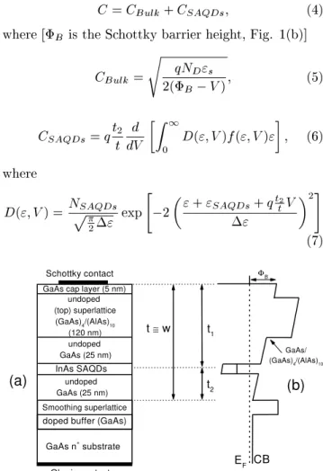
Figure1. Panel (a) shows a skethof the samplesand in
panel(b)is showntheorrespondingskethofthe energy
banddiagram.
B
istheShottkybarrierheight,E
F isthe
Fermienergy.
Intheaboveequations,D(";V)istheeletron
den-sity of states, f(";V) is the Fermi-Dira energy
dis-tribution, t2
t
V the voltage aross the quantum dots.
Theloaldensityof statesin theInAs SAQDsanbe
written in adelta funtion form in the idealase (no
dots size dispersion); here, we should inlude the
agaussianbroadeningofthedensityofstates[10℄with
a harateristi energy dispersion ". "
SAQDs is the
exitation energy of the trapped eletrons in SAQDs.
NotiethatC
SAQDs
alsotakesintoaounttheeets
ofthe temperaturewhihare inludedintothe F
ermi-Diradistribution.
Asabovementionedandinaordanewitheqs. (4)
and (6) apaitane measurements are well suited for
investigationson thedensityof statesand onthe
sys-temdimensionality. Thissituationisdiretlyobserved
inthelowtemperaturelimit(T !0)whereC
SAQDs is
welldesribedby[11, 12℄
C
SAQDs =
t
2
t q
2
D("
F )+
2
6 (kT)
2
2
" 2
F D("
F )+
7 4
360 (kT)
4
4
" 4
F D("
F )+:::
; (8)
d
where"
F
istheFermienergy. Inthisase,thetunneling
isthedominantmehanismoftheharging/disharging
proessoftheeletronstatesintheSAQDs. Underthe
abovesimplifying onditions(no durrentowingin
thestrutureandnoband bending)theapaitaneis
adiret method of measuringtheDOS[12℄.
Consider-ing only the rst term of the expansion in eq. (8) in
powersofkT,weareabletousetheDOS-apaitane
relantionship in order to identiate the
dimensional-ityof aneletronsystem. However,eq. (8) should be
arefullyused(inaqualitativeapproah)beauseinan
interatingsystem(astheSAQDs)theDOSdependson
thenumberofeletronsin thesystem.
The eletrial oupling established in eq. (4) also
reetstheinompletesreeningoftheeletrieldby
all parts of thestruture. The nonabruptedge of the
depletionregionallowsasmalltailoftheeld to
pen-etrate through the rst barrier [width t
1
; Fig. 1(b)℄
into the SAQDs plane. Thus, when the eletri eld
isdepleting therstbarrier,theSAQDsregion isalso
ontributing to the apaitane. The distribution of
eletronsintheplaneoftheSAQDswillnotsreen
en-tirelytheeldwhihpenetratesintotheseondbarrier
[width t
2
,Fig. 1(b)℄. Thenat agivenvoltage applied
to the Shottky ontat all parts of the struture are
ontributing to the measured apaitane. Certainly,
theeletrial ouplingbetweenthebarriers and
quan-tum dots depends on the interlayer distanes and on
thedopingleveloftheseregions.
IV Results and disussion
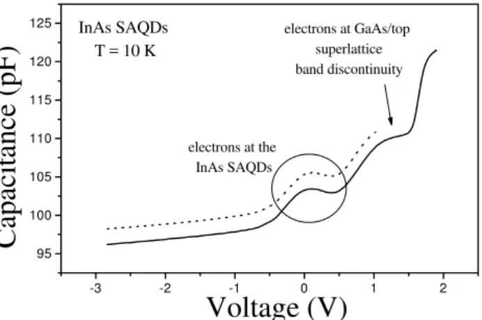
Next,weappliedthemodeltottheexperimentalC-V
urves. Fig. 2 shows both the experimental and
the-oretial urves. The measuredapaitane shows two
distintregions: awelldenedpeakinthevoltagerange
from-0.8 to0.2V andaplateaulikedependene from
0.5to1.5V.Thisseondregionwillbedisussedlater.
Thebehaviorof theapaitanein therstrange an
be explained as follows: starting at V = -0.8 V, the
measuredapaitaneinreasesduetothellingofthe
dots,showingapeakatV=-0.11V(thepeakisbroad
reases, the apaitanesignaldiminishes beause the
dotsare ompletelylledand forafurther inreaseof
theappliedvoltage,thetotalapaitaneisgivenbythe
ontributionof thebulkGaAs. Fromeq. (6),whereit
wasusedagaussianfuntiontodesribethedensityof
states, thepeakobserved in theC-V urvesis an
evi-deneofan eletronsystemharaterizedbya
dimen-sionality lowerthan two. Sine wedo not expet the
presene of an one-dimensional system, it seems lear
that thenegativedierentialapaitaneinthe-0.8to
0.2 V voltagerange onrmsthepresene ofquantum
dots,thusrevealingitszero-dimensionalharater. Eq.
(4)wasnumeriallysolvedinthelowtemperaturelimit
(8) using "
SAQDs
and " as tting parameters. The
tting proess was limited to the voltage range from
the1.0Vto-3.0V,where theontributionofthedots
dominatestheapaitaneofthestruture. Themodel
reproduestheexperimentalbehaviorandthetted
pa-rametersof thezero-dimensionalgaussian distribution
werefoundtobe" C V
SAQDs
=110meV and" C V
=94
meV (Fig. 2).
-3
-2
-1
0
1
2
95
100
105
110
115
120
125
InAs SAQDs
T = 10 K
electrons at the
InAs SAQDs
electrons at GaAs/top
superlattice
band discontinuity
Capacitance (pF)
Voltage (V)
Figure2. Experimental(solid line)andalulated (dotted
line) apaitane-voltage urvesfor the sample with InAs
SAQDs. Thenegativedierentialapaitanebetween-0.8
and 0.2Vis anevideneof thezero-dimensionalharater
ofthequantumdots.
As it is well established, the magnitude of the
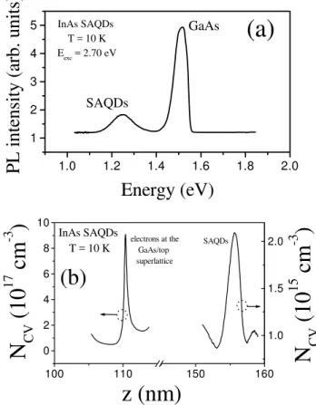
trum [10℄. Fig. 3(a) shows the PL measurements
takenat 10K.Weonlyobservetheluminesenelines
related with the eletron-hole reombination in the
SAQDs (E = 1.24 eV) and in the GaAs (E = 1.51
eV). The energy E = 1:24eV with an energy
broad-ening of 111 meV (obtained by agaussian t),
orre-sponds to an eletron level loated at 90 meV below
the ondution band of GaAs. It was alulated
us-ing the disontinuity energy for the ondution band
E
CB
=0:85(E
GaAs E
InAs
). Theother peakat
E =1:51eV is assoiatedwiththelumineseneofthe
bulk GaAs. Theexitation energy ("
SAQDs
) and the
width (") ofthe PLline assoiatedwiththeSAQDs
were found in aordane with the apaitane
mea-surements(" PL
SAQDs
=90meV and" PL
=111meV).
This isavalidation oftheproposedmodelforthe
al-ulation oftheapaitane-voltageurves.
Dueto thesampleonstrutiongeometry,the
ele-trons an also be loalized forming a 2DEG in both
(GaAs)
4
=(AlAs)
11
=GaAs top interfae (indiated in
Fig. 1) and in thewettinglayer. Infat,weobserved
the presene of this kind of eletron onnement on
themeasuredapaitaneasevidenedbytheinrease
of the apaitaneand the plateau observed from 0.5
V to 1.5 V in Fig. 2. This observation is in
aor-dane with the well dened relationship between
a-paitaneanddensityofstates:atwodimensional
ele-tron gas(2DEG) presentsastep-likedensityof states
whihshouldprodueaplateau-likedependeneforthe
apaitane-voltageurves[12℄.
Someexperimentalfatsallowedustoonludethat
theobservedplateaushould berelatedto theonned
eletronsatthe(GaAs)
4
=(AlAs)
11
=GaAstopinterfae:
thePLmeasurementsplottedinFig. 3(a)didnotshow
evidenesoftheontributionofthewetting-layerwhih
was onrmed by additional Raman sattering
mea-surements, as we reently reported [13℄. Also, there
is no evidene of the exited states of the SAQDs in
boththePLspetrumandC-Vmeasurements. By
ap-plying a forward bias to the sample, a 2DEG at the
(GaAs)
4
=(AlAs)
11
=GaAs top interfae is formed and
a plateau is observed in the C-V urves. At a high
enoughvoltagethe 2DEGis depletedof eletronsand
a derease of the apaitane is observed in the C-V
urves(Fig. 2).
An additional onrmation of the origin of the
plateau in the measured apaitane an be obtained
from the alulation of the spatial distributionof the
harges in this sample alulating the C-V prole
[14, 15℄,
N
C V (z)=
2
qS 2
"
s
dC 2
dV
1
; (9)
and
z=S "
s
; (10)
where N
C V
is the density of eletrons at z. A very
sharppeakin the eletrondensitywasobtainedwhen
using the eq. (9) to alulate the prole [Fig. 3(b)℄.
Thispeakat z=110nmreetstheeletron
aumu-lation at the GaAs/topsuperlattie as expeted from
theanalysisof theC-Vurves.
100
110
150
160
0
2
4
6
8
10
electrons at the
GaAs/top
superlattice
SAQDs
InAs SAQDs
T = 10 K
(b)
N
CV
(10
17
cm
-3
)
z (nm)
1.0
1.2
1.4
1.6
1.8
2.0
1
2
3
4
5
GaAs
SAQDs
(a)
InAs SAQDs
T = 10 K
E
exc
= 2.70 eV
Energy (eV)
PL intensity
(arb. units)
1.0
1.5
2.0
N
CV
(10
15
cm
-3
)
Figure3. (a)PLspetrumofthesamplewithInAsSAQDs
atT=10K.ThelinesatE=1.24eVandE=1.54eVare
relatedtotheSAQDsandGaAsbulkluminesenes,
respe-tively. Panel (b)shows the eletronditribution along the
growth diretion. It was alulated usingthe
apaitane-voltagedata.
In the voltage range where the negative
dieren-tial apaitane is dominant, the onventional
equa-tions [eq. (9) and eq. (10)℄ for the C-V alulation
are not valid and thus we use an alternative method
asdesribedinourpreviouswork[5℄. Inthefollowing
somerelevantaspetsofthisnewmethodaregiven. An
alternativeand diret wayfor the onstrution of the
C-Vproleinoursamplesisthealulationofageneral
expressionfor thespatial eletroni distribution along
thestrutureasafuntion ofthetotalapaitane:
N
C V
(w)=F(C)F(w) (11)
with
C=G(C
Bulk ;C
SAQDs
) (12)
where w is the depletion region, F, G are unknown
eq. (11) is only possible to obtain if there is a well
dened relation between the apaitane and the
de-pletionwidth. Inaquantumdotssystem,thisrelation
annotbedeterminedbeausethedepletion
approxima-tionisnotvalidforasystemwithdimensionalitylower
than3[theeqs. (9) and(10)were deduedin this
ap-proximation℄. Inotherwords,anexpressionwhihgives
therelation between theeletrondistribution andthe
apaitanelikeeq. (9) is notpossible to be ahieved
forasystemontainingquantum dots.
Desribingthesystem(dots)asapureeletrostati
systemembeddedin abulk struture, thedependene
between the distribution of eletrons and apaitane
allowedus to determinetheform offuntion F as
fol-lows[5℄:
N
CV =
C 3
Bulk
q"
s
dC
Bulk
dV
1
1+ qt
1
"
s n
V
(13)
with
w= "
s
C
Bulk
S; (14)
where C
Bulk
is the apaitane of the bulk struture
without quantum dots. Notie that eq. (13) an be
writenas
N
CV =F
1 (C
Bulk )+F
2 (C
SAQDs
); (15)
where
F
1 (C
Bulk ) =
C 3
Bulk
q"
s
dC
Bulk
dV
1
(16)
F
2 (C
SAQDs ) =
"
C 3
Bulk
q"
s
dC
Bulk
dV
1 #
qt
1
"
s n
V
(17)
This means that the unknown dependene of the
onned eletronsupon thewidth of thedepletion
re-gionisdeterminedbytheprodutindiatedinfuntion
F
2 (C
SAQDs
) above. The dependene of the funtion
F
2 (C
SAQDs
)onthenominalpositionofthedotsplane
(t
1
) give an unertainty in the amplitude of the C-V
prole. It is worthwhile to notie two points: rstly,
we onsideralinearform for theunknownfuntion G
whih states the dependene of the total apaitane
[C = C
Bulk +C
SAQDs
, in eq. (12)℄ on the bulk and
dotsapaitane;seondly,thedotsontributionineq.
(13)isproportionaltothe apaitaneofthedotsper
unity of harge and area, and impliitly ontains the
dimensionalityoftheonnedsystemthroughthe
den-sityofstates.
Using the model desribed above, the C-V prole
wasalulatedandthepeakatz=155nmreetsthe
[Fig. 3(b)℄. Thedensityofeletronsin the plane
on-tainingthe dotsanbe obtainedfrom theC-V prole
by the integration of the N
C V
w urves [16℄: an
averagevaluen'510 9
m 2
wasfound.
In summary, this paper presented a study of the
apaitane-voltage harateristis in the InAs
quan-tum dotssystem embedded in anundoped GaAs
ma-trix. The proposed model reprodues essential
fea-tures of the studied system and it was based on
the analysis of the solution of the Poisson's equation
and in the well dened relationship between
apai-tane and density of sates. As a result, the
ontri-butions of the eletrons onned in zero- (SAQDs),
bi- [(GaAs)
4
=(AlAs)
11
=GaAs interfae℄ and
three-dimensional (bulk) states were distinguished in the
measuredapaitane. Inaddition, the energy
disper-sion and the eletronexitation energy of theSAQDs
wereobtained in loseagreementwith the
photolumi-nesenemeasurements.
TheauthorswouldliketoaknowledgeE.Diagonel
for hishelp with thesamplepreparation.The nanial
support of Brazilian agenies CNPq and FAPESP is
alsoaknowledged.
Referenes
[1℄ M.Grundmann,O.Stier,andD.Bimberg,Phys.Rev.
B52,11969(1995).
[2℄ R.C.Ashoori,H.L.Stormer,J.S.Weiner,L.N.
Pfeif-fer,S.J.Pearton,K.W.Baldwin,andK.West,Phys.
Rev.Lett.68,3088(1992).
[3℄ G. Medeiros-Ribeiro, D. Leonard, and P. M. Petro,
Appl.Phys.Lett.66,1767(1995).
[4℄ S.Anand,N.Carlsson,M.E.Pistol,L.Samuelson,and
W.Seifert,Appl.Phys.Lett.67,3016(1995).
[5℄ A.J.Chiquito,Yu.A.Pusep,S.Mergulh~ao,J.C.
Galz-erani, and N. T. Moshegov, Phys. Rev. B 61, 5499
(2000).
[6℄ H. Drexler, D. Leonard, W. Hansen, J. P.Kotthaus,
andP.M.Petro,Phys.Rev.Lett.73,2252(1994).
[7℄ T. P. Smith III, K.Y.. Lee, C. M. Knoeldler, J. M.
Hong,andD.P.Kern,Phys.Rev.B38,2172 (1988).
[8℄ Ph. Lelong, O. Heller, G. Bastard, Physia E 2, 678
(1998).
[9℄ J. M. Lopez-Villegas, P. Roura, J. Bosh, J. R.
Morante, A. Georgakilas, and K. Zekentes, J.
Ele-trohem.So.140,1492(1993).
[10℄ P. N. Brounkov, A.A. Suvorova, N. A. Bert, A. R.
Kovsh, A. E.Zhukov,A. Yu.Egorov,V. M. Ustinov,
A.F.Tsatsulnikov,N.N.Ledentsov,P.S.Kopev,S.G.
Konnikov, L. Eaves, and P. S.Main, Semiondutors
32,1096(1998).
[11℄ K.Hatori, J.Appl.Phys.78,4543(1995).
[12℄ S.Luryi,Appl.Phys.Lett.52,501(1988).
[13℄ Yu. A.Pusep, G.Zanelatto, S. W.Silva, J.C.
[14℄ E. H. Rhoderik and R. H. Williams,
Metal-semiondutorContats(Oxford,Cambridge),1988.
[15℄ P.Blood,Semiond.Si. Teh.1,1(1986).
[16℄ E. F. Shubert, Semiondutors and Semimetals Vol.