Strain and Relaxation Processes in In
1,xGa
xAs
yP
1,y/ InP
Single Quantum Wells Grown by LP-MOVPE
A.A. Bernussi, W.Carvalho Jr.,M.T.Furtado, and A.L. Gobbi
Fundac~ao Centro de Pesquisa e Desenvolvimento em Telecomunicac~oes Fundac~ao CPqD / Associac~ao Brasileira de Tecnologia de Luz Sncrotron-ABTLuS
13088-061 Campinas, SP, Brazil
Received February 6, 1999
Strained and partially relaxed In1,xGaxAsyP1,y/InP single quantum wells (SQWs) with dierent
cap layer thicknesses and biaxial strain values grown by low-pressure metalorganic vapor phase epitaxy (LP-MOVPE) were investigated by double crystal X-ray diraction, photoluminescence microscopy (PLM) imaging and photoluminescence spectroscopy techniques. Our results indicate a signicant improvement of the optical quality of the quaternary wells with increasing values of the cap layer thickness. Tensile and compressive strained In1,xGaxAsyP1,y/InP SQWs grown with
the same structure exhibited dierent relaxation processes, even when the strain magnitude was the same. PLM images of highly compressive quantum wells exhibited a large number of dark lines corresponding to mist dislocations as a result of the partial relaxation process in the well material. PLM images of similar tensile strained samples revealed only the presence of dark spots with no evidence of mist dislocations.
I Introduction
Strained-layer In1,xGaxAsyP1,y quaternary alloys
grown on InP substrates have been widely used as ac-tive layers in optoelectronic devices, mainly in long wavelength semiconductor lasers and electroabsorption modulators for optical communication systems. The introduction of a biaxial strain into the active region of multiple-quantum well laser diodes and modulators resulted in improved electro-optic performances as com-pared with similar ones employing lattice-matched qua-ternary materials[1]. Although high quality InGaAsP strained layers have been successfully obtained by dif-ferent growth techniques, the strain relaxation mech-anisms involved in these structures are still unclear. If a critical thickness is exceeded, plastic relaxation of the elastic energy can occur through generation of mist dislocations. More recently, relaxation through elastic mechanisms was observed in tensile strained In-GaAsP/InP structures, where the strain relief takes place via surface undulations along [110]direction. This elastic relaxation process was found to be strongly de-pendent on the growth temperature and on the growth rate[2-4]. It has been reported evidence of strain re-covery in partially relaxed InGaAs/GaAs single
quan-tum wells (SQWs) with increasing cap layer thickness, suggesting that the cap layer thickness should be also considered as a parameter to determine critical layer thickness in lattice mismatched SQWs[5].
The aim of this contribution is to investigate the ef-fects of the cap layer thickness and the sign of the strain on the relaxation processes of strained and partially re-laxed InGaAsP/InP SQWs grown by low-pressure (LP) metalorganic vapor phase epitaxy (MOVPE). Our anal-ysis is mainly focused on the optical properties of qua-ternary strained materials using photoluminescence mi-croscopy (PLM) imaging and photoluminescence (PL) spectroscopy techniques.
II Experimental details
Strained InGaAsP/InP SQWs were grown in a Thomas Swan LP-MOVPE horizontal reactor equipped with a fast vent-run switching manifold. The samples were grown on InP:S (100)-oriented substrates at 70 Torr pressure and at a growth temperature of 670oC.
tempera-ture in the range of 1250-1350nm and nominal strain values () of=0:75% and=1:0%:
The structures were ended with an undoped InP cap layer (dcap) with thicknesses varying from 5 to 500nm. The PLM imaging system uses the 514.5nm line of an argon ion laser as the excitation source. The spa-tial resolution of the PLM imaging apparatus is about 1m. Integral luminescence radiation emitted from the
samples was collected and imaged into a lead-sulde infrared (IR) camera. The laser excitation power used was in the range of 1 to 500W/cm2. All PLM
measure-ments were performed at room temperature.
Spectrally resolved PL measurements were per-formed at 12K temperature using the 514.5nm line of an argon ion laser with an excitation power in the range of 10,3% to 10+2 W/cm2. The emitted PL radiation
was dispersed by a 0.75m grating monochromator and the detection was obtained by a liquid-nitrogen cooled Ge photodetector using a standard lock-in technique. Double crystal X-ray diraction experiments were car-ried out on (200) reection using Cu-K1 radiation.
In1,xGaxAsyP1,y biaxial strain values and alloy
com-positions were determined by combining results of X-ray and PL measurements.
III Results and discussion
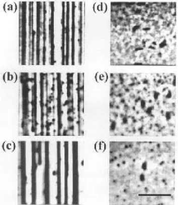
Fig. 1 shows the PLM images of compressive ( =
+0:90%) and tensile ( = ,0:98%) strained
In-GaAsP/InP SQWs with dierent cap layer thicknesses. PLM images of compressive strained SQWs (Figs.1a-1c) revealed a large number of dark lines that were at-tributed to mist dislocations. The occurrence of plas-tic relaxation in these samples indicates that the well thickness exceeded the critical layer thickness. As the cap layer is increased the density of dark lines slightly decreases. This suggests an increase of the residual strain in compressive strained SQWs. PLM images of tensile strained SQWs (Figs.1d-1f) exhibited the pres-ence of dark spots with no evidpres-ence of mist disloca-tions. The dark spots were attributed to crystal de-fects acting as non- radiative centers, strongly quench-ing the luminescence in the extent of the carrier dif-fusion length. The dark spot density is almost three orders of magnitude higher than the etch pit density measured on the InP:S substrate, indicating that they are not correlated with threading dislocations originat-ing at the substrate[6]. PLM images (not shown) of InGaAsP/InP SQWs with strain values of= +0:70%
and = ,0:75% exhibited only the presence of dark
spots without any evidence of mist dislocations. The results shown in Fig.1 indicate a signicant dierence in the strain relaxation processes in In-GaAsP/InP SQWs grown with essentially the same structure and strain magnitude but having opposite signs. In the case of compressive strained SQWs with
= +0:90% a plastic deformation occurs trough the
creation of mist dislocations. On the other hand, strain relaxation in tensile structures with=,0:98%
takes place via elastic processes and can be explained by the lateral composition modulation caused by the mis-cibility gap of the quaternary alloy, which favors phase separation during growth into InAs- and GaP-rich re-gions[7].
Figure 1. PLM images of compressive strained,= +0:90%,
InGaAsP/InP SQWs with cap layer thicknesses of (a) 5nm, (b) 100nm and (c) 400nm, and tensile strained,=,0:98%,
InGaAsP/InP SQWs with cap layer thicknesses of (d) 5nm, (e) 100nm and (f) 400nm. Marker represents 100m.
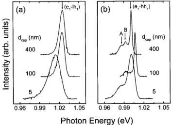
In order to provide additional informationabout the relaxation processes on strained InGaAsP/InP SQWs, we show in Fig.2 the results of low temperature PL mea-surements (normalized to unity) performed on the same samples analyzed in Fig.1. The PL spectra of tensile strained SQWs (Fig.2a) exhibited a single emission line corresponding to the fundamental transition between rst electron and light-hole states (e
1 ,l h
1). When the
increases and the full width at half maximum(FWHM) decreases from 21.1 meV to 10.6 meV, respectively. The PL spectra of compressive strained SQWs (see Fig.2b) exhibited three emission lines. The main peak located at the high-energy side was attributed to the transition between rst electron and heavy-hole states (e
1 ,hh
1).
The remainder peaks labeled as A and B are located
at 14 meV and 8 meV below the fundamental
QW e 1
,hh
1 transition, respectively and their origin
will be discussed later. Again, the increase of cap layer thickness in compressive strained SQWs resulted in im-proved material quality. As the cap layer is increased from 5 to 400 nm the PL intensity increases and the FWHM corresponding to thee
1 ,hh
1transition is
re-duced from 10.6 meV to 3.9 meV, respectively. The PL results exhibited in Fig.2 clearly indicate that sam-ples grown with larger d
cap values exhibited narrower
PL linewidths. Variations in PL peak positions with increasing d
cap values shown in Fig.2 are attributed
to dierences in the alloy compositions between sam-ples. A larger PL linewidth was observed for all ten-sile strained samples grown with dierent d
cap values
when compared to similar compressive strained sam-ples. This behavior is due to larger composition uc-tuations caused by phase separation during growth of tensile quaternary alloys into of InAs- and GaP-rich re-gions [7].
The remarkable reduction of PL linewidth with cap layer thickness can be explained by an improvement of the interface quality and to a decrease of the quaternary alloy composition uctuation during growth of the bi-nary cap layer. Samples grown with larger cap layer thicknesses require longer growth times. As a conse-quence, strained quaternary well materials experience longer annealing times. A possible explanation for the observed PL linewidth reduction with cap layer thick-ness is the sharpening of lateral composition modula-tion interfaces caused by the thermal annealing pro-cess[8]. Also, the annealing process tends to homoge-nize regions of dierent alloy compositions.
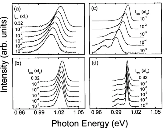
In order to identify the origin of the additional features observed in compressive strained SQWs (see Fig.2b), the excitation power dependence of the PL spectra at low temperatures of these samples, and the corresponding tensile strained ones, were investigated. Figs.3a and 3b shows the PL spectra (normalized to unity) of tensile strained SQWs with d
cap = 5 and
100nm, respectively, as a function of excitation
inten-sity. When the excitation intensity is increased by four orders of magnitude, thee
1 ,l h
1PL peak energy of the
tensile strained SQW sample with d
cap=5nm (Fig.3a)
shifted by 14.0 meV towards higher energies. At the same excitation intensity range a negligible shift of the
e
1 ,l h
1 PL peak energy was observed for the tensile
strained sample with d
cap = 100nm. The excitation
power dependence of the compressive strained SQW sample with d
cap = 5nm (Fig.3c) showed a shift of
the e 1
,hh
1 PL peak energy as large as 31.1 meV
towards higher energies. Also, as the excitation in-tensity increases the relative inin-tensity of the spectral featureAdecreases and almost vanishes at higher
exci-tation power levels. Similarto the tensile strained SQW with larged
cap layer, a negligible PL peak energy shift
was observed on the compressive strained sample with
d
cap = 5nm. However, the relative intensity of
tran-sitions A and B decreases with the excitation power
intensity.
Figure 2. PL spectra at T=12K of (a) tensile strained,
= ,0:98%, and (b) compressive strained, = +0:90%,
InGaAsP/InP SQWs with dierent cap layer thicknesses.
The intensity saturation of low-energy A and B
PL emissions (see Figs.3c and 3d) suggest that defects might be involved in these transitions[9]. Similar PL experiments were performed on compressive strained SQWs with = +0:70% and with dierent dcap
val-ues. The PL spectra (not shown) of those samples ex-hibited only a single emission band corresponding to thee
1 ,hh
1 transition and no evidence of low- energy
features were observed. The above results and those obtained in Figs.1a-1c provide additional support that transitions observed below the e
1 ,hh
1 peak energy
Figure 3. PL spectra at T=12K at dierent excitation power levels of tensile strained InGaAsP/InP SQWs, =,0:98%,
with (a)dcap= 5nm and (b)dcap=100nm, and compressive strained InGaAsP/InP SQWs,= +0:90%, with (c)dcap= 5nm
and (d)dcap= 100nm.
The strong PL peak energy shift with excitation power observed on strained InGaAsP/InP SQWs sam-ples with d
cap = 5nm (see Figs. 3a and 3c) can be
tentatively explained by a decrease of the surface band bending. As the excitation intensity increases, optically created minority carriers move toward the surface and recombine with charges trapped in surface states. This reduces the net charge at the cap layer surface and then reduces the built-in electric eld. As a consequence, the PL peak energy shifts to higher energies. On the other hand, strained quantum wells grown with larger d
cap
values are less sensitive to the built-in electric eld and exhibited a negligible PL energy shift with excitation intensity.
IV Conclusions
Strained and partially relaxed strained InGaAsP/InP single quantum wells with dierent strain values and dierent cap layer thicknesses were investigated by PL, PLM and high resolution X-ray diraction techniques. Plastic relaxation was observed in highly compressive strained SQWs through the generation of mist dislo-cations. Similartensile strained SQWs exhibited elastic
relaxation processes via composition uctuations. In-creased values of the cap layer thickness resulted in im-proved optical quality of the analyzed samples. Near-surface strained InGaAsP/InP SQWs exhibited pro-nounced PL peak energy shift with power excitation. This eect was attributed to a reduction of the surface built-in electric eld.
Acknowledgements
The authors gratefully acknowledge the technical assistance of Mr. L.C. Silveira Vieira and Mr. H. Gazetta Filho.
References
[1] P.J.A. Thijs, J.J.M. Binsma, L.F. Tiemeijer and T. van Dongen, IEEE J. Quantum Electron.30, 477 (1994).
[2] A. Ponchet, A. Rocher, J.-Y. Emery, C. Starck and L. Goldstein, J. Appl. Phys.77, 1977 (1995).
[3] T. Okada and G.C. Weatherly, J. Crystal Growth179,
339 (1997).
[4] W. Carvalho Jr., A.A. Bernussi, M.T. Furtado and A.L. Gobbi, unpublished.
[6] A.A. Bernussi, W. Carvalho Jr., M.T. Furtado and A.L. Gobbi, unpublished.
[7] R.R. LaPierre, T. Okada, B.J. Robinson, D.A. Thomp-son and G.C. Weaterly, J. Crystal Growth 155, 1
(1995).
[8] C.K.W. Wyllie and D.A. Thompson, Semicond. Sci. Technol. 13, 750 (1998).