Abstract— Nowadays, optical amplifiers designs are induced by
new requirements generated by optical networks. The introduction of WDM reconfigurable networks with increasing rate from 10-40 Gb/s to 100 Gb/s and beyond, demand new optical amplifiers development with improved gain spectral flatness and noise figure for all operational range of input powers and set-point gains. In this paper, it was developed a hybrid distributed Raman/EDFA amplifier with a novel hybrid gain control (HGC) scheme based on joint actuation. The HGC was firstly developed by numerical simulation and after experimentally, in a WDM system with 100 km SSMF fiber span and full C-band load. The Results shows an improved equivalent noise figure with flattened gain spectrum for all amplifier operation range in dynamic optical networks.
Index Terms— Hybrid optical amplifier, Automatic gain control, EDFA, Raman amplifier, WDM reconfigurable optical networks.
I. INTRODUCTION
Optical amplifiers are key elements in wavelength and waveband routed dynamic DWDM (dense wavelength division multiplexing) networks. While the capacity of optical transmission systems is increasing with higher bit rates and more complex modulation schemes to meet growing bandwidth demand [1], large changes in channel loading or input powers of optical amplifiers can result in faults in branching networks [2]. Then, dynamic gain control to provide spectral gain flatness becomes a fundamental feature for optical amplifiers operating in reconfigurable optical networks [2].
The two-stage erbium doped fiber amplifier (EDFA) with coupled automatic gain control (AGC) [3] is mostly used as an optical amplifier topology to provide variable AGC with flattened spectral gain for dynamic optical DWDM networks. Unfortunately, flat spectral gain for the full range of controlled gain values is achieved only at the expense of degraded noise figure (NF) [3], [4]. This NF penalty is particularly detrimental because advanced modulation formats for high-rate channels (100 Gb/s and beyond) are being widely deployed, imposing a better noise performance in optical amplifiers [1], [2], [5].
Thereby, there is a clear need to develop new optical amplifier structures with variable AGC, to provide both, flat spectral gain with lower NF, for the complete AGC gain set point range, as well as
Hybrid Distributed Raman/EDFA Amplifier
with Hybrid Automatic Gain Control for
Reconfigurable WDM Optical Networks
Juliano R. F. Oliveira, Uiara C. Moura, Júlio C. R. F. Oliveira
Centro de Pesquisa e Desenvolvimento em Telecomunicações – CPqD, Campinas, Brasil {jrfo,umoura,julioc}@cpqd.com.br
Murilo A. Romero
for the full amplifier input power operation range.
In this paper, it is proposed a hybrid optical amplifier topology and developed a novel hybrid gain control (HGC) through computational simulation tool, and experimentally, applying the HGC in a distributed Raman amplifier (DRA)/EDFA hybrid topology. This novel gain control is based on the use of a simultaneous and complementary way of an AGC EDFA and an on-off AGC DRA [6].
Considering the improved noise characteristics provided by the DRA and the EDFA high amplification efficiency providing high output power, it was shown in [7] that the DRA/EDFA hybrid amplifier can provide an improved performance in reconfigurable WDM networks.
The Paper Structure is organized as follow: Sec. II presents the simulated design of hybrid amplifier optical circuit and AGC for each stage (DRA and EDFA), and the developed HGC for the hybrid DRA/EDFA through joint actuation. Sec. III presents the experimental hybrid amplifier design. In Sec. IV, the hybrid amplifier performance is evaluated (equivalent noise figure, flatness gain spectrum, and AGC accuracy) for all defined dynamic operation range, experimentally and by simulation. Sec. V presents the results and discussion and finally, Sec. VI presents the conclusions.
II. SIMULATION HYBRID AMPLIFIER DESIGN
Due the long simulation time required to use feedback AGC in optical amplifiers through the optical simulation tool (Optisystem®), it was developed a forward AGC EDFA, and a
feed-forward AGC (on-off gain) DRA, and using both the HGC for the proposed hybrid amplifier was developed [6]. To develop feed-forward AGC, it was necessary to perform a previous amplifier characterization using the optical simulation tool, and from the results it was extracted the feed-forward AGC equations. Then, each simulated AGC amplifier (and hybrid amplifier with HGC) was made by implementing the feed-forward control loop in MATLAB® assisting the simulation tool. In
this section, the optical circuits for simulated EDFA and DRA amplifiers are presented. Also, it is detailed the designed AGC for each amplifier, and the designed HGC for simulated hybrid amplifier.
A. EDFA Design and Gain Control
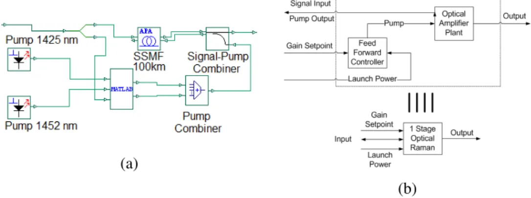
The EDFA module and its feed-forward AGC control loop were developed as shown in Fig. 1. In Fig. 1(a) the designed EDFA optical circuit to provide high output power with average NF is shown, which consists in a single co-propagating EDFA stage with 980 nm wavelength pump with 500 mW of nominal optical power, that is combined with the input signal through an integrated tap/isolator/pump coupler (1.4 dB of insertion loss for signal and 0.6 dB for pump), followed by 14 m of Erbium doped fiber (EDF), isolator, tap (99%/1%) and a pump remove filter, with 0.8 dB of combined insertion loss. The EDF length was designed to provide best gain spectral flatness at 17 dB.
Fig. 1(b) illustrates the feed-forward AGC control loop, which is implemented inside the simulated EDFA MATLAB box, illustrated in Fig. 1(a).
over the total input power varying from 0 to -30 dBm with 0.5 dB step, and over the pump power varying from 10 mW to 500 mW with 80 steps in a logarithm scale [4]. The channel loading was 40 channels (full C-band load), ranging from 192.1 THz to 196.0 THz (worst load scenario). This simulation procedure lasts 21 hours for the designed EDFA, but is made one time only. After this, the simulated feed-forward AGC run in 18 seconds instead 1200 seconds for simulated feedback AGC.
(a)
(b)
Fig. 1. (a) feed-forward AGC EDFA implemented on software simulation tool, (b) feed-forward AGC EDFA control loop. To generate the AGC feed-forward coefficients, the characterization results are processed for each gain setpoint from the target setpoint range, generating a five degree polynomial equation, which calculates the pump power (mW) level to provide requested gain depending on EDFA input total power (dBm), as illustrated in Fig. 1(b). Then, simulated feed-forward AGC EDFA provides the desired gain, executing the Fig. 1(b) feed-forward AGC control loop inside Fig. 1(a) MATLAB box.
B. Distributed Raman Amplifier Design and Gain Control
The DRA gain stage was developed as shown in Fig. 2(a), with the feed-forward on-off AGC control loop illustrated in Fig. 2(b). Fig. 2(a) represents the simulated DRA designed to provide low equivalent NF and spectral gain flatness in SSMF (G.652) fiber span (higher than 60 km). The DRA consists in two counter-propagating pumps at 1425 nm and 1452 nm wavelengths, each with 250 mW maximum optical powers, combined with signal input through a pump coupler with 1.5 dB of signal insertion loss and 0.6 dB pump insertion loss.
(a)
(b)
Fig. 2. (a) Distributed Raman amplifier with feed-forward on-off AGC implemented on software simulation tool, (b) Distributed Raman amplifier feed-forward on-off AGC control loop.
Fig. 2(b), the DRA was previously characterized by the simulation tool.
The characterization procedure is similar to the performed for EDFA in Sec. II-A [4], but now use a two level nested parameter simulation over the total launch power (varying from -10 dBm to 20 dBm with 0.5 dB step), and over 1425/1452 nm pump powers (varying from 0 mW to 250 mW (100%) for 1424 nm pump and 181 mW (72.4%) for 1452 nm), for 80 steps in a logarithm scale (the pumps power tilt is applied to provide a more flattened DRA gain spectrum). The same input channel loading (full C-band) was used. This simulation procedure lasts around 57 hours for the designed DRA but, as in EDFA design, it is needed to be executed only one time to characterize the designed DRA.
The developed MATLAB script processes the characterization results and generates for each on-off gain setpoint (from 0 dB to 10 dB) a five degree polynomial equation, to calculate the pump powers (mW) needed to provide the on-off gain requested in function of the DRA input power (dBm) with pumps off, as illustrated in Fig. 2(b). Moreover, the simulated DRA provides on-off AGC for requested setpoint gain, running the Fig. 2(b) feed-forward on-off AGC inside the Fig. 2(a) MATLAB box. This feed-forward controller calculates the DRA pump powers needed to provide the requested gain based on the DRA input power with pumps off (launch power minus span attenuation loss). After the characterization process, the simulation time for DRA with on-off AGC run in 60 seconds.
C. Hybrid DRA/EDFA Design and Gain Control
The simulated hybrid amplifier is illustrated in Fig. 3(a), and the feed-forward HGC control loop is illustrated in Fig. 3(b). In Fig. 3(a), the proposed simulated hybrid amplifier is composed firstly by a counter-propagating DRA with on-off feed-forward AGC designed in Fig. 2(a), and an EDFA with feed-forward AGC designed in Fig. 1(a), and a intermediate gain flattened filter (GFF).
(a) (b)
Fig. 3. (a) Distributed Raman/EDFA hybrid amplifier simulation layout with HGC, (b) Distributed Raman/EDFA hybrid amplifier hybrid automatic gain control loop.
Because of this, the GFF must provide flat gain spectrum for the EDFA at the nominal gain of 17 dB. To reach higher gain values, a designed flat gain spectrum DRA is used to provide the complementary gain (from 0 dB to 10 dB), covering the hybrid amplifier setpoint gain range from 17 dB to 27 dB with flat spectrum gain. Additionally, DRA improves the effective NF of the proposed hybrid amplifier due the distributed gain at the transmission span [1]. This way, the hybrid amplifier with HGC will provide a flat spectrum gain with better NF than a two stage EDFA with coupled AGC (most used variable gain flattened amplifier) [3], for any gain setpoint inside the gain range.
For hybrid gain control loop illustrated in Fig. 3(b), the HGC is executed in two separated and simultaneous phases. At first phase, each amplifier stage control their gain in a separated way. The EDFA always makes nominal gain control (17 dB), and the hybrid setpoint gain is complemented by DRA on-off AGC, providing the remaining gain needed calculated through Equation (1).
Raman setpoint nominalEDFAgain
G G G (1)
Where GRaman represents the DRA on-off target gain, Gsetpoint is the hybrid amplifier target setpoint
gain and GnominalEDFAgain is the EDFA nominal stage gain. For desired higher gain range, the nominal
power of Raman pump laser or the number of pumps must be increased.
III. EXPERIMENTAL HYBRID AMPLIFIER DESIGN
The HGC for hybrid amplifier was implemented by a Raman pump module with embedded EDFA [10]. This amplifier provides EDFA feed-back AGC with ASE compensation at output power of the EDFA amplifier stage, and pump powers level control for Raman counter-propagating pumps.
Using this amplifier module, it was implemented a DRA on-off AGC through the blind estimation of DRA input power with pumps off, and the polynomial equations to adjust the Raman pumps power to provide the on-off gain requested for spans with SSMF (G.652) fiber (≥ 60 km).
This section will describe the experimental hybrid amplifier topology developed, followed by the Raman on-off AGC and the DRA/EDFA HGC implemented to control the hybrid amplifier.
A. Raman amplifier pump module with embedded EDFA
Fig. 4(a) illustrates the optical circuit topology for experimental hybrid amplifier. This optical circuit is similar to the previously simulated hybrid amplifier, illustrated in Fig. 3(a).
(a)
(b)
(c)
The hybrid amplifier is composed by two counter-propagating Raman pumps at 1425 nm and 1452 nm wavelengths with up to 500 mW of total combined output power [10], and a single stage EDFA with co-propagating pump at 980 nm wavelength. The GFF position is the first difference between simulated and experimented hybrid amplifier (GFF in experimental optical amplifier is positioned at the amplifier output). The second difference between the experimental and simulation optical amplifier is related to the EDFA AGC method, on the experimental amplifier the AGC make the ASE noise compensation, where in the simulated one the AGC does not make the ASE noise compensation.
The experimental EDFA AGC used was the feedback AGC with amplified spontaneous emission (ASE) compensation available at amplifier module, provides an AGC with better accuracy than the simulated feed-forward AGC.
Fig. 4(b) illustrates the feedback AGC with ASE compensation control loop. The ASE calculation is made through a feed-forward characterized equation in function of input power and gain setpoint [11]. The ASE power is added to currently gain setpoint generating the new gain setpoint to provide the gain with ASE compensation [11] (the ASE compensation extends the dynamic range). This new gain setpoint is then subtracted to the real measured gain (output power minus input power), and a proportional integrate (PI) controller actuates at the pump power to reach the setpoint gain.
The DRA stage feed-forward on-off AGC illustrated in Fig. 4(c) is carried out through a blind estimation of the total output Raman off power [6], avoiding the need to turn off Raman pumps to measure the on-off gain. This blind estimation is made through the Equations (2) and (3).
RamanOut Raman Attenuation
LaunchEst
P PD
G
Span
(2)OffEst LaunchEst Attenuation
P P
Span
(3)Where PLaunchEst is the launch power estimated, PDRamanOut is the Raman amplifier output power,
GRaman is the Raman on-off gain, SpanAttenuation is the span attenuation and POffEst is the Raman amplifier
output power estimated with Raman pumps off. The feed-forward DRA on-off AGC continuously actuates at DRA pumps level to assure the desired on-off gain, through polynomial fit equation (one equation per set point gain).
The coefficients for DRA AGC polynomial fit were obtained characterizing the DRA, only one time per each fiber type (spans≥ 60 km), through the automatic amplifiers and/or optical system characterizer showed in Fig. 6(b). The on-off AGC DRA algorithm, recursively running, controls precisely the on-off gain of the DRA. After three iterations, the maximum gain error is 0.5 dB [6].
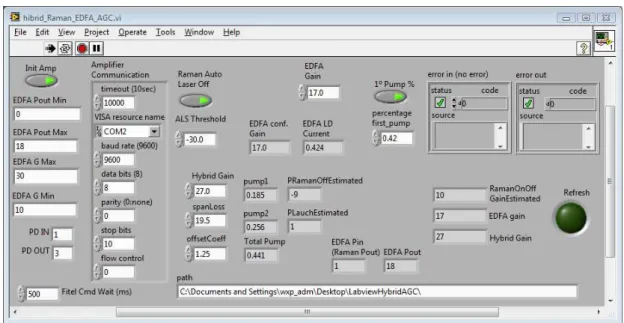
B. Experimental HGC Labview© Implementation
The experimental amplifier with HGC was implemented in a Labview© graphical user interface
(GUI) illustrated in Fig. 5. This GUI is able to communicate with the amplifier module through RS-232, to configure module operation mode, read module status, and actuate on module pump lasers.
To implement the amplifier HGC, firstly the GUI calculates through Equation (1) the DRA on-off AGC setpoint, and configure the EDFA AGC to nominal setpoint gain (17 dB). Then with provided span loss information, a blind estimation of DRA output power with Raman pumps off is made through Equations (2) and (3), and the DRA on-off AGC illustrated in Fig. 4(c) is implemented in GUI, using the polynomial fit equations developed in Sec. II-B.
Fig. 5. Experimental hybrid amplifier Labview control GUI.
IV. HYBRID AMPLIFIER PERFORMANCE EVALUATION
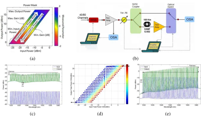
To evaluate the hybrid amplifier performance regarding to parameters such as channels NF, gain spectral flatness and AGC accuracy, it is needed to adjust the amplifier input power and gain to obtain, for each amplifier operation point, the input and output power spectrums in order to calculate such parameters. A simulation and experimental evaluation tool were designed for this purpose. Before describe these tools, it is needed to define the amplifier power mask concept, which is an important concept about optical amplifier performance evaluation for dynamic WDM network.
A. Amplifier Power Mask
Amplifiers in a reconfigurable WDM network scenario should work for an input power range that covers different channel loads and/or input power variations, once in these networks the input power changes in a dynamically and unpredictable way. Furthermore, these amplifiers must operate with AGC for a setpoint gain range required for amplifiers operating in dynamic WDM networks.
Fig. 6(a). For each input/output total power operation point, the amplifier performance is described by the NF (or equivalent NF for Raman amplifiers), gain flatness spectrum and AGC accuracy values.
(a) (b)
(c) (d) (e)
Fig. 6. (a) Optical amplifier power mask and (b) Experimental setup for optical amplifier performance evaluation, (c) High gain, low total in/out spectrum (d) Power mask result example (flatness) and (e) Low gain, high in/out power spectrum. To determine the power mask optical amplifier performance with respect to those parameters, it is necessary to obtain several points inside it and evaluate them, in a process called amplifier characterization. With this aim in mind, an amplifier/systems characterizer was designed for both the simulated hybrid amplifier and the experimental hybrid amplifier [13].
B. Experimental Characterization
The power mask defined for the hybrid amplifier deployed in this paper was the region limited by the following parameters: Minimum input power = -28 dBm; Maximum output power = 18 dBm; Minimum gain = 17 dB; Maximum gain = 27 dB.
The experimental setup of the characterization is shown in Fig. 6(b), which initially consists of a channels equalizer loop that adjusts all 40 channels lasers (from 192.1 to 196 THz) to provide a flat spectrum at the auxiliary amplifier output.
In Fig. 6(b) the system evaluated consists of 100 km of SSMF G.652 (19 dB of span loss) and the hybrid amplifier. At the auxiliary amplifier output used to provide sufficient launch power to the system, a variable optical attenuator (VOA) is adjusted to provide system launch power from -8 to 20 dBm, that after attenuates along the fiber span, reaches -28 to 1 dBm when Raman pumps are off. A 50%/50% coupler provides the system input power to the tested system and to the optical spectrum analyzer (OSA), where a controlled optical switch is used to select the spectrum to be read (input test system spectrum or output test system spectrum).
input signal a power equalized full C-band load with 100 GHz channel spacing (40 channels). Each point illustrated at Fig. 6(d), was obtained by the characterizer through processing input and output power spectrums (two samples are showed in Fig. 6(c) and Fig. 6(e)), to calculate worst channel NF or equivalent NF (for amplifiers with distributed Raman technology), gain flatness spectrum (output channel peak difference), and AGC accuracy (difference between measured and target AGC).
During the characterization process, a remote routine sends information to adjust the input power and the amplifier gain, with a 1 dB of granularity between points, and records the input and output spectrum for all power mask points, which totalizes 220 points for the power mask mentioned above.
C. Simulated Characterization
The simulated setup is simpler than the experimental (Fig. 6(b)) because there is no need to use components such as channels equalizer loop, auxiliary amplifier, 50%/50% coupler and optical switch at the simulation environment.
The same experimental characterization process was made in simulation, using a full C-band load and 1 dB of granularity for each point regarding input power and amplifier gain variation.
V. RESULTS AND DISCUSSIONS
This section presents the results and discussions over the simulation and experimental power mask performances obtained respectively for both designed hybrid amplifiers with HGC at simulation and experimental.
Power mask results for the simulated hybrid amplifier with HGC are illustrated in Fig. 7 and Fig. 9, and the power mask results for the experimental hybrid amplifier are illustrated in Fig. 8 and Fig. 9.
To show the hybrid amplifier with HGC spectrum flatness gain performance for all AGC setpoint gain range (17 to 27 dB), and for the maximum input power range that allows these gains (-18 to -9 dBm), total input power operation points at the power mask were suitable chosen considering the simulated and experimental power mask.
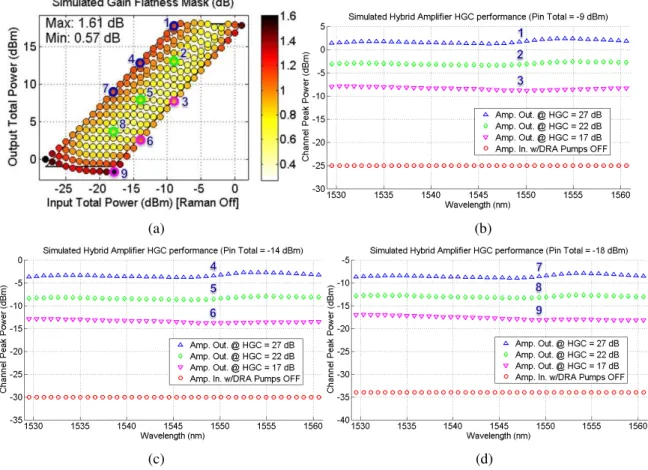
For the designed hybrid amplifier at simulation, the Fig. 7(a) illustrates the simulated gain flatness spectrum power mask, where the horizontal axis represents the total input power measured (or estimated) with the Raman pumps power turned off, and the vertical axis represents the total output power. The rate between the vertical and horizontal axis provides the on-off gain level provided by the simulated hybrid amplifier, and the color bar at Fig. 7(a) represents the gain spectrum flatness measured for this operation point based on the maximum channels peak power difference at amplifier output considering a flattened spectral input.
The spectrum flatness gain provided by the simulation hybrid optical amplifier, vary only 1.04 dB for all simulated hybrid amplifier power mask, providing a good flatness power mask performance.
(a) (b)
(c) (d)
Fig. 7. (a) Simulated hybrid amplifier flatness power mask and HGC spectral performance evaluation for three different gains setpoints and following total input powers: (b) -9 dBm (c) -14 dBm (d) -18 dBm.
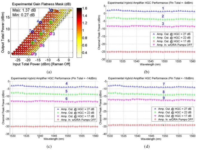
For designed experimental hybrid amplifier, Fig. 8(a) illustrates the experimental gain flatness spectrum power mask. The spectral flatness gain resulted from the experimental hybrid amplifier with HGC, ranges from 0.27 to 1.37 dB for the amplifier operating in a 100 km SSMF span.
For the points indicated in Fig. 8(a) ranging from 1 to 9, they are spectrally detailed in Fig. 8(b), 8(c) and 8(d), showing respectively the experimental C-band gain spectrum behavior, for the AGC setpoint gain range for three different input total power with Raman pumps off (-9 dBm, -14 dBm and -18 dBm).
The spectrum flatness gain provided by the experimental hybrid optical amplifier, vary only 1.1 dB for all simulated hybrid amplifier power mask, which is approximately the same variation obtained at the simulation hybrid optical amplifier, but with better flatness level (minimum of 0.27 dB against 0.57 dB, and maximum of 1.37 dB against 1.61 dB at simulation).
The experimental hybrid optical amplifier provides very good flatness power mask performance, allowing this amplifier to operate in reconfigurable optical WDM networks, this result is way better then a single stage EDFA with AGC [4].
(a) (b)
(c) (d)
Fig. 8. (a) Experimental hybrid amplifier flatness power mask and HGC spectral performance evaluation for three different gains setpoints and following total input powers: (b) -9 dBm (c) -14 dBm (d) -18 dBm.
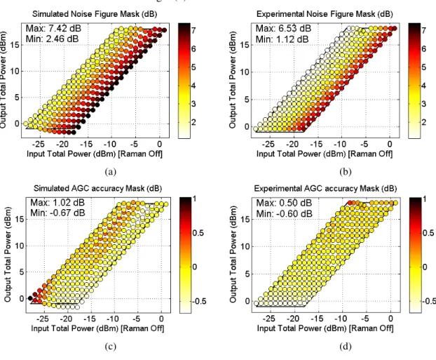
Figs. 9(a) and 9(b) shows the equivalent noise figure (NF) power mask performance, respectively for the simulated and the experimental hybrid optical amplifier with HGC.
As can be seen in Figs. 9(a) and 9(b), experimental hybrid amplifier equivalent NF range from 1.12 to 6.53 dB while the simulated hybrid amplifier ranges from 2.46 to 7.42 dB, this way the experimental amplifier provides better NF than the simulated one. This occurs mainly because the different placement of GFF in Figs. 4(a) and 3(a). A loss element placed at output end has less influence on the total system NF than is placed in the middle of the amplified system.
The experimental NF also is way better than the two stage EDFA with VOA amplifier topology NF [4]. This is expected because comparing the two stage EDFA with VOA amplifier topology to the hybrid amplifier, one EDFA stage and VOA was exchanged by a DRA Stage, removing two signal degrade elements for a DRA stage.
see the better performance of the experimental hybrid amplifier AGC accuracy (-0.6/+0.5 dB) when is compared to the simulated case (-0.67/+1.02 dB). This mainly occurs due the experimental amplifier use of feedback AGC shown in Fig. 4(d) for the EDFA stage, which is very accurate due the steady state no gain error provided by the PI feedback gain control algorithm, while the simulated EDFA use a feed-forward AGC illustrated in Fig. 1(b) which is more inaccurate.
(a) (b)
(c) (d)
Fig. 9. Simulated amplifier power masks results related to noise figure (a) and AGC accuracy (c). Experimental amplifier power masks results related to noise figure (b) and AGC accuracy (d).
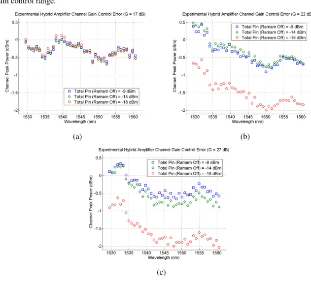
Despite the total automatic gain control (AGC) accuracy illustrated by Figs. 9(c) and 9(d) for the simulated and experimental hybrid amplifier with HGC respectively, Figs 10 and 11 illustrates the channel AGC accuracy for the same total input powers with Raman pumps off (-9, -14 and -18 dBm) and setpoint gains (17, 22 and 27 dB) were the spectral flatness was previously analyzed, for both simulated and experimental designed hybrid amplifier respectively.
(a) (b)
(c)
Fig. 10. Simulated hybrid amplifier channel gain error for several total input powers (with Raman pumps off), considering the following adjusted setpoint gains: 17 dB (a), 22 dB (b) and 27 dB (c).
Analyzing the illustrated results in Figs. 10 and 11, it can be seen that considering the evaluated setpoint gains (17, 22 and 27 dB) for the simulated and experimental hybrid optical amplifier with HGC, the obtained channel gain control error values was around +0.5/-1.0 dB for the input powers of -9 and -14 dBm, providing a good performance for the use of this amplifier in reconfigurable WDM optical networks.
However, analyzing Figs. 10 and 11 illustrated results regarding to the channel gain control error for the total input power (with Raman pumps off) of -18 dBm, and 22 and 27 dB of HGC setpoint gain, it can been see that in these cases, the channel gain control error exceed 1 dB, reaching in both simulated and experimental hybrid optical amplifier 2 dB gain control error.
This control gain error occurs mainly because the nature of DRA on-off AGC, that performs the gain control using the total output power and the total input power, then making no distinction between signal and amplified spontaneous emission (ASE), and then, for low signal input power at the hybrid amplifier DRA, the ASE appears with high level when compared to the amplified signal level, then even performing the total gain control correctly, the ASE disturbs the channel gain control.
DRA on-off AGC part from the hybrid optical amplifier with HGC to extend the dynamic channel gain control range.
(a) (b)
(c)
Fig. 11. Experimental hybrid amplifier channel gain error for several total input powers (with Raman pumps off), considering the following adjusted setpoint gains: 17 dB (a), 22 dB (b) and 27 dB (c).
Then, in this section it was presented that the experimental hybrid amplifier with novel HGC presents low NF in the high gain region of the power mask as illustrated in Fig. 9(b), with values of flatness, up to 1.37 dB as illustrated in Fig. 8(a). The good performance parameters are achieved along all the dynamic operation range (for total gain control), with maximum values of 6.53 dB and 1.37 dB for NF and flatness respectively. The hybrid amplifier with HGC can provide spectral gain flatness allied with very low NF when compared against the two stages EDFA with coupled AGC control [3], [4].
VI. CONCLUSION
This improved equivalent noise figure with flattened gain spectrum for full C-band load allows its use on the new reconfigurable optical networks with advanced modulation formats for 100 Gb/s and beyond.
ACKNOWLEDGMENT
Thanks for financial support of FUNTTEL, FINEP and CPqD Foundation.
REFERENCES
[1] J. T. Rahn et al., “250gb/s real-time pic-based super-channel transmission over a gridless 6000km terrestrial link,” in
OFC, 2012, p. PDP5D.5.
[2] G. Sacchi et al., “Design and experimental characterization of edfa-based wdm ring networks with free ase light
recirculation and link control for network survivability,” J. Lightwave Technol., vol. 23, no. 3, p. 1170, Mar 2005.
[3] M. Abu Bakar et al., “Variable gain-flattened l-band erbium-doped fiber amplifier,” Laser Physics, vol. 21, pp. 1638–
1644, 2011.
[4] G. E. R. Paiva et al, “Metodologia de Projeto de EDFAs de Alto Desempenho para Redes WDM Reconfiguráveis,”
MOMAG, 2012.
[5] B. Zhu et al., “Recent progress in transmission fibers for capacity beyond 100-tbit/s,” in OFC, 2012, p. OW1D.5.
[6] J. R. F. de Oliveira et al., “Hybrid Distributed Raman/EDFA Amplifier with Novel Automatic Gain Control for Reconfigurable WDM Optical Networks,” MOMAG, 2012.
[7] J. R. F. de Oliveira et al., “Amplificador Óptico híbrido para redes wdm reconfiguráveis com formatos de modulação
avançados e recepção coerente,” Caderno CPqD Tecnologia, vol. 7, no. 2, pp. 59–74, July- December 2011.
[8] J. Dung, H. Cheng, and Y. Syu, “Gain stability in a distributed raman amplifier for a wavelength-division multiplexing
system,” Optical Engineering, vol. 49, p. 045003, 2010.
[9] M. Pal et al., “Study of gain flatness for multi-channel amplification in single stage edfa for wdm applications,” Optical
and Quantum Electronics, vol. 39, pp. 1231–1243, 2007.
[10]Raman Pump Module with Embedded EDFA, Fitel/Furukawa, 2010.
[11]A. F. Herbster et al., “Extensão da faixa dinâmica por meio da correção da ase aplicada a edfas em redes Ópticas wdm,”
MOMAG, 2008.
[12]Multichannel Erbium-Doped Fiber Amplifier (EDFA), JDSU, 2009.
[13]U. C. Moura et al, “Caracterizador Automatizado de Máscara de Potência de Amplificadores Ópticos para Redes WDM
Reconfiguráveis,” SBrT, 2012.