738 Brazilian Journal of Physics, vol. 29, no. 4, December, 1999
Electronic Coupling and Thermal Relaxation in
Self-assembled InAs Quantum Dot Superlattices
E. Petitprez, N.T. Moshegov, E. Marega Jr., P. Basmaji,
Departamento de Fisica e Ci^encia dos Materiais - IFSC - USP
Caixa Postal 369 - 13560-970 S~ao Carlos, SP, Brazil
A. Mazel, D. Dorignac, and R. Fourmeaux
CEMES/CNRS, BP 4347 31055 Toulouse Cedex 04, France
Received February, 1998
We report optical and structural characterizations of InAs quantum dot superlattices grown by molecular beam epitaxy on GaAs (001). Cross-sectional electron microscopy imaging reveals20
nm diameter InAs islands well aligned along the growth direction. Low temperature photolumi-nescence spectra exhibit a clear redshift with decreasing island vertical separation, as a result of electronic coupling between stacked dots, given that the larger shift is obtained for 70 A spacing. At high excitation power, the photoluminescence spectra show a doublet structure corresponding to coupled and uncoupled quantum dot states. The temperature dependence of the photolumines-cence indicates that thermionic emission activation energy is much lower than the estimated barrier height. Such a dierence is explained by the presence of non-radiative recombination centers due to strain relaxation and In segregation.
I Introduction
Self-organized semiconductor growth has recently gained considerable interest due to the possibilities it oers as an alternative formation of quantum dot (QD) structures, avoiding post-growth processing techniques drawbacks. QD arrays produced in this way have been extensively investigated by optical[1-3], structural[4,5] and electrical[6,7] measurements, showing their poten-tiality to act as optoelectronic devices. Although QD laser operation has already been demonstrated[8-10], the degree of uniformity achieved in single layer QD structures still leads to a signicant gain bandwidth broadening[11]. The growth of QD superlattices has then been considered as a way to increase QD arrays uniformity. Such structures surprisingly exhibit a ver-tical self-organization, since new islands tend to nucle-ate directly above the buried ones due to local surface strain minima[12,13]. Recent results also suggest that QD stacking leads to more uniform island size distri-bution[14,15]. Moreover, the formation of vertically or-dered QD stacks allows to exploit electronic coupling of the islands by controlling the inter island separation thickness[16]. In this paper we report on photolumines-cence (PL) investigations of InAs QD superlattices (SL) grown by molecular beam epitaxy (MBE) with
dier-ent GaAs spacer layer thicknesses. Transmission elec-tron microscopy (TEM) is used to image QD vertical alignment. The optical results suggest electronic cou-pling is best achieved for a given spacer layer thickness. For this specic thickness, coupled and uncoupled elec-tronic states are observed. Finally, thermal relaxation is found to occur via non-radiative defects centers.
II Growth and
experimentalde-tails
The structures were grown by conventional molecular beam epitaxy on (100) GaAs substrates under an As4
background pressure of 210
,6 Pa. InAs and GaAs
rates were set to 0.1 and 0.35 monolayer (ML)/s, re-spectively. The whole growth process was controlled in situ by reection high energy electron diraction (RHEED). After oxide desorption, a 0.3m thick GaAs
buer layer was grown at 580 oC, followed by ten
pe-riods of an AlAs(5ML)/GaAs(10ML) superlattice, and then by a 0.1m GaAs layer. Next, the substrate
tem-perature was lowered to 450 oC and 3 InAs ML were
E. Petitprezet al. 739
structures. Variations of the RHEED specular beam intensity at InAs growth initial stages indicated the for-mation of a complete InAs monolayer. At 1.8 ML InAs coverage, spots appeared on the RHEED pattern due to 3D island formation, followed by a rapid fall-o of the specular beam intensity. During GaAs spacer layer de-position, the specular beam intensity rst did not vary and then gradually increased, presenting superimposed oscillations. Meanwhile, the 3D island spots slowly dis-appeared, revealing the (24) GaAs surface
reconstruc-tion pattern. The structure was nally capped with a 500 A GaAs layer. A single QD layer sample was also grown with the same conditions for reference purpose.
The samples were prepared for cross-sectional TEM observations by conventional mechanical polishing and ion milling techniques, and then observed with a PHILIPS CM30ST microscope under an acceleration voltage of 300 kV. PL investigations were performed in a closed cycle He cryostat under Ar+laser green line
ex-citation (514.5 nm). The optical emission spectra were analyzed by a 0.5 m single grating spectrometer and measured in lock-in mode by a photomultiplier.
III Results and discussion
Fig. 1 presents a cross-sectional TEM image of a 3 layer QD superlattice sample taken along the [2] zone axis. The spacer layer is 50 A. The strain contrast clearly reveals 20 nm diameter lens-shaped InAs island
for-mation for all layers, conrming RHEED observations. No structural defects, such as QD non-formation, mi-crotwins or dislocations could be observed. As ex-pected, QDs align vertically in stacks. Moreover, in some cases, QDs in the upper layer seem larger than those in the rst layer. Since QD size modication has a considerable inuence on PL peak position, it is there-fore important to determine whether such phenomenon really occurs. Unfortunately, due to rather thick sam-ples, high resolution TEM images did not permit to determine precisely QD lateral sizes.
Figure 1. Dark-eld (g= 200) cross-sectional TEM
micro-graph of a 3-layer QD SL sample.
Fig. 2 shows measured PL spectra for 3-layer QD superlattices with 130, 100 and 70 A GaAs spacer
lay-ers. A single QD layer PL spectrum is also presented for comparison. The main peak is due to electron-hole QD ground state recombination. Stacking a few QD lay-ers slightly redshifts the PL peak. Decreasing spacer layer thickness down to 70 A also clearly drives the optical emission towards lower energies. Stacking in-duced strain relaxation accounts for part of this band gap reduction. Additionally, wave-function overlap al-lows electronic coupling between the islands, and thus lowers the QD ground state energy level. Closer is-lands are expected to produce stronger coupling, hence shifting the PL peak towards lower energies for sam-ples with thinner spacer layers. Fig. 3 summarizes PL peak position behavior as a function of GaAs spacer layer thickness for the two series of samples. As dis-cussed earlier, PL spectrum experiments a redshift as the spacer layer is reduced from 130 to 70 A due to electronic coupling between nearby dots. Surprisingly, as the spacer layer further decreases, the optical emis-sion is blue-shifted. We therefore conclude there exists a certain spacer layer thickness for which coupling is best attained, and that this thickness is about 70 A. We suggest that strain relaxation in too closely stacked islands allows QD lateral size modication along the vertical direction, what, in turn, inhibits coupled states formation.
Figure 2. PL spectra of a single QD layer (dotted line) and of 3-layer QD SL samples with 130 (squares), 100 (circles) and 70 A (diamonds) GaAs spacer layers.
740 Brazilian Journal of Physics, vol. 29, no. 4, December, 1999 dominate the spectrum. A linear dependence with
ex-citation density is derived for both peaks, hence we do not attribute any of them to an impurity-assisted ra-diative recombination. Furthermore, these two peaks cannot arise from dierent QD size distribution since both of them should be observable with the same in-tensity ratio in the whole excitation density range.
Figure 3. PL peak position as a function of GaAs spacer layer thickness. Solid and open squares refer to 3- and 7-layer QD superlattices, respectively.
Figure 4. Excitation density inuence on a 3-layer QD SL sample with 70 A spacer layer. Excitation density was 10 (squares), 30 (circles), 65 (up triangles), 130 (down trian-gles), and 190 (diamonds) KW/cm2. Inset shows the two
gaussian components used for tting.
In multilayered samples, the apparition of new PL peaks with increasing excitation density has been at-tributed to optical emission from excited states[17]. For a single set of 20 nm diameter QDs, theoretical and experimental results show that the rst excited state transition occurs 50 to 80 meV above the ground state transition[18,19]. As the energy dierence between the two peaks of g. 4 is about 50 meV, optical recombi-nation from excited states could be responsible for the PL peak doublet structure. However, in closely stacked QD layers, vertical electronic coupling between nearby dots has to be considered. The calculated ground state energy lowering due to such coupling ranges between 20 and 50 meV[20,21], and the rst excited state, even lowered by the coupling, lies well above the uncoupled ground state[20]. We therefore attribute these low- and high-energy peaks to coupled an uncoupled QDs, re-spectively. As in Ref. [22], we suppose uncoupled states arise from QD lateral size variations within the vertical stack. Coupled states, due to their lower ground state, are rst populated. With increasing excitation density, all coupled states become populated and radiative re-combination also occurs via uncoupled states. At high excitation densities, this recombination process domi-nates due to the lower density of coupled QD states.
E. Petitprezet al. 741
high-energy gaussian component. The inset shows the two gaussian components at 15 K.
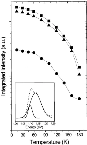
PL measurements as a function of temperature were also carried out to investigate thermal relaxation pro-cesses in these samples. All samples exhibited a good thermal stability and a good PL signal could be de-tected up to 180 K. Fig 5 presents integrated PL inten-sity temperature dependence of a 7-layer QD SL. The two gaussian components exhibit the same tempera-ture stability, but slightly dierent behavior because of the dierent degree of wave function localization in the coupled and uncoupled states. From these plots were extracted the PL quenching activation energies. For low- and high energy peak, respectively, we obtained 38 and 78 meV, leading to a 40 meV dierence, which is very close to the 36 meV PL peak position dierence (see g. 5 inset). PL quenching process is therefore the same for coupled and uncoupled states. However, these values are much smaller than the estimated InAs-GaAs barrier height[23]. Similarly, the obtained values ranged from 30 to 108 meV for all samples. We there-fore suppose that PL quenching does not arise from car-rier thermionic emission to the GaAs barcar-rier but from non-radiative recombination centers. Such centers may originate from strain-induced structural defects, as well as from interface defects due to In segregation.
IV Conclusion
We have investigated electronic coupling and thermal relaxation in QD superlattices with dierent GaAs spacer layer thicknesses by PL measurements. The ground-state transition energy of the stacked QDs is found to decrease with decreasing spacer thickness as a result of the higher degree of strain relaxation and elec-tronic coupling. For very closely stacked QDs, strain relaxation inhibits electronic coupling by modifying is-land lateral size. PL quenching activation energies are found to be considerably smaller than the estimated barrier height, indicating that thermal quenching oc-curs through carrier non-radiative recombination via defect states.
Acknowledgments
This work is supported by the Fundac~ao de Am-paro a Pesquisa do Estado de S~ao Paulo (FAPESP) and the Conselho Nacional de Desenvolvimento Cientico e Tecnologico (CNPq), Brazil.
References
[1] S. Fafard, R. Leon, D. Leonard, J.L. Merz, and P.M. Petro, Superlatt. Microstruc.16, 303 (1994).
[2] D. Leonard, M. Krishnamurthy, C.M. Reaves, S.P. Denbaars, and P.M. Petro, Appl. Phys. Lett.63, 3203
(1993).
[3] D. Leonard, S. Fafard, K. Pond, Y.H. Zhang, J.L. Merz, and P.M. Petro, J. Vac. Sci. Technol. B 12, 2516
(1994).
[4] M. Grundmann, J. Christen, N.N. Ledentsov, J. Bohrer, D. Bimberg, S.S. Ruvimov, P. Werner, U. Richter , U. Gosele, J. Heydenreich, V.M. Ustinov, A.Y. Egorov, A.E. Zhukov, P.S. Kopev, and Z.I. Alferov, Phys. Rev. Lett.74, 4043 (1995).
[5] R. Notzel, T. Fukui, H. Hasegawa, J. Temmyo, A. Kozen, and T. Tamamura , Chem. Vap. Dep. 1, 81
(1995).
[6] H. Drexler, D. Leonard, W. Hansen, J.P. Kotthaus, and P.M. Petro, Phys. Rev. Lett.73, 2252 (1994).
[7] G. Medeiros-Ribeiro, D. Leonard, and P.M. Petro, Appl. Phys. Lett.66, 1767 (1995).
[8] R. Mirin, A.C. Gossard, and J.E. Bowers, Physica E2,
738 (1998).
[9] K. Kamath, N. Chervela, K.K. Linder, T. Sosnowski, H.T. Jiang, T. Norris , J. Singh, and P. Bhattacharya, Appl. Phys. Lett.71, 927 (1997).
[10] N. Kirstaedter, O.G. Schmidt, N.N. Ledentsov, D. Bimberg, V.M. Ustinov, A.Y. Egorov, A.E. Zhukov, M.V. Maximov, P.S. Kopev, and Z.I. Alferov, Appl. Phys. Lett.69, 1226 (1996).
[11] M. Grundmann and D. Bimberg, Jap. J. Appl. Phys. Part 136, 4181 (1997).
[12] Q. H. Xie, P. Chen, and A. Madhukar, Appl. Phys. Lett.65, 2051 (1994).
[13] Q. H. Xie, A. Madhukar, P. Chen, and N.P. Kobayashi, Phys. Rev. Lett.75, 2542 (1995).
[14] J. Terso, C. Teichert, and M.G. Lagally, Phys. Rev. Lett.76, 1675 (1996).
[15] G. S. Solomon, S. Komarov, J.S. Harris, and Y. Ya-mamoto, J. Cryst. Growth175, 707 (1997).
[16] G. S. Solomon, J.A. Trezza, A.F. Marshall, and J.S. Harris, Phys. Rev. Lett.76, 952 (1996).
[17] Q. H. Xie, N.P. Kobayashi, T.R. Ramachandran, A. Kalburge, P. Chen, and A. Madhukar, J. Vac. Sci. Tech-nol. B14, 2203 (1996).
[18] M. Grundmann, N.N. Ledentsov, O. Stier, J. Bohrer, D. Bimberg, V.M. Ustinov, P.S. Kopev, and Z.I. Alferov, Phys. Rev. B53, 10509 (1996).
[19] K. H. Schmidt, G. Medeiros-Ribeiro, M. Oestreich, P.M. Petro, and G.H. Dohler, Phys. Rev. B54, 11346
(1996).
[20] L. C. Fonseca, J.L. Jimenez, and J.P. Leburton, Phys. Rev. B58, 9955 (1998).
[21] M. Colocci, A. Vinattieri, L. Lippi, F. Bogani, M. Rosa-Clot, S. Taddei, A. Bosacchi, S. Franchi, and P. Frigeri, Appl. Phys. Lett.74, 564 (1999).
[22] R. Heitz, A. Kalburge, Q. Xie, M. Grundmann, P. Chen, A. Homann, A. Madhukar, and D. Bimberg, Phys. Rev. B57, 9050 (1998).
![Fig. 1 presents a cross-sectional TEM image of a 3 layer QD superlattice sample taken along the [2] zone axis.](https://thumb-eu.123doks.com/thumbv2/123dok_br/18978658.456215/2.918.503.803.611.833/presents-cross-sectional-image-layer-superlattice-sample-taken.webp)