Abstract— In this letter, a new transition between microstrip line and substrate integrated waveguide in Ku-band frequency is proposed. This transition composed of one row of not metallized air-vias drilled on both sides of the microstrip line with taper end. The electromagnetic analysis is carried out using a commercial software tool. The presented transition achieves return losses better than 41 dB in Ku-band frequency (12.4-18GHz). In order to validate the simulated results of the proposed concept, a back-to-back transition prototype is designed, fabricated and measured. The measured results demonstrate a minimum return loss of 29.05 dB and maximum insertion loss of 0.685 dB over the entire Ku-band frequency.
Index Terms—Substrate Integrated Waveguide; Microstrip Line; Tapred
Transition; Air-Vias
I. INTRODUCTION
The emerging technology of substrate integrated waveguide (SIW), a veritable paradigm,
considering migration from metal walls waveguides to the planar technology. In its simplest form, its
two cylinder rows between two metals plates which can confine the electromagnetic field. Since the
microstrip line is very practical in many configurations, including active components connectivity, the
trend is to merge it in the same substrate with SIW, geometrically irreconcilable structures. This requires
the development of transitions, junctions and couplings, with high technical quality, and therefore
implies performing a good calculation model. These transitions are very important for the matching of
impedance and field between the SIW and planar circuits. D. Deslandes et al. proposed the first
transition between microstrip and SIW with taper form [1]. H. Nam et al. proposed a transition
microstrip-to-SIW in Ku-band frequency range [2], in this transition, the return loss is about 15 dB and
bandwidth is 24%. In the past years, several works about the transition between SIW and microstrip line
or coplanar waveguide have been developed ([3-8]). In [9] another transition from microstrip-to-SIW is
proposed. This transition are formed by placing two vias symmetrically at either side the microstrip
taper, this vias and the SIW vias, have the same diameter. In Ku-band frequency, this transition gives
return losses better than 35dB.
Ku
-
band Transition with not Metalized Air
-Vias between Microstrip Line and
Substrate Integrated Waveguide
Farouk Grine , Mohamed Taoufik Benhabiles and Mohamed Lahdi Riabi
Laboratoire des électromagnétismes et télécommunication, Université de Constantine 1, Route d'Ain El Bey, Constantine 25000, Algerie
Farouk Grine; [email protected]
Furthermore, in this letter, a new transition between microstrip line and SIW structure is
introduced. This transition constructed by placing one row of not metallized air-vias on both sides of the
microstrip line. In Ku-band frequency (12.4 to 18 GHz), the new transition has been studied in two
different substrate and it gives return losses better than 41 dB. In order to verify the proposed scheme a
back-to-back transition was fabricated.
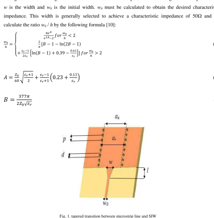
II. MICROSTRIP TRANSITION
The microstrip line is one of the most used transmission lines in the conception of microwave
systems. The topology of the structure transition between microstrip line and substrate integrated
waveguide is shown in figure 1.This transition has three main parameters: the length l of the tapered form,
w is the width and w0 is the initial width. w0 must be calculated to obtain the desired characteristic
impedance. This width is generally selected to achieve a characteristic impedance of 50Ω and we
calculate the ratio w0 / h by the following formula [10]:
� ℎ =
{
�
�− ���ℎ <
�[ − − ln − +��−
�� {ln − + . −
. �� }] ��
� ℎ >
(1)
= √
��++
��−��+
. +
.
��
(2)
=
√��� (3)
Thus, as "h " is the substrate height, it becomes easy to calculate the value of w0. It remains now
the value of two other transition parameters to calculate. The w must be calculated by equating the two
right sides of the equations (4) and (5) and solving it (we is the width of an equivalent waveguide) [11]:
�
= {
ɳℎ
ln
ℎ�
+ . 5
� ℎ �
ɳℎ[�ℎ+ . + . ln �ℎ+ .
(4)
�
=
.
− . ��+ +��−��
√ + ℎ�
(5)
For the parameter l we can use a simpler method by choosing the median width between the microstrip
line and the end of the transition, as follow:
w
median= (
w + w
0) / 2
(6)It suffices to calculate the wavelength for this width and set the length to aquarter of wavelength. We
must first find the effective dielectric constant for this microstrip line width [11]:
� =
��+−
��−√ + �� ���ℎ
(7)
We must then calculate λc with the following equation:
�
�=
√� � ��(8)
III. PROPOSED TRANSITION STRUCTURE AND DESIGN
The new transition we propose is achieved by drilling one row of not metallized air-vias on both sides of
the microstrip line with taper form. Fig. 2 presents the transition between microstrip and SIW. In this
figure the configuration ends with regular waveguide. Fig. 2(a) presents the transition without air-vias on
both sides of the microstrip line. The new microstrip-SIW transition with not metallized air-vias is
presented in Fig. 2(b) and
(c).
In this figure,
a
SIW is the SIW width, Wequi is the equivalent width, d is thediameter of vias, p is the vias inter-distance, wt is the width of taper form, wm is the width of the
microstrip line, and lt is the length of taper form. In this study, two structures have been investigated. In
the first one, the substrate is made of RT/duroid 6002 with electric permittivity
ε
r=
2.94, loss tangent of0.0012. In the second structure, the dielectric is chosen as Rogers RO3003 with
ε
r=3,
loss tangent of0.0013, and the substrate height is h=0.508 mm for both taper-via transitions and taper not metallized
air-vias transition.
Because the fields in the microstrip line are concentrated near the line, only one row of air-vias is
this new structure, is that there is better field matching between the SIW and micosrtip due to the
confinement of the fields around the microstrip line. In order to validate this configuration we compare
with taper transition without air-vias proposed in [9]. The structure consists of SIW substrate with ten
metallized vias and thirteen not metallized air-vias at the both sides of the microstrip line. The width of
SIW is obtained directly from [12], and the effective width can be calculated as:
r c equif c
w
2
(9)
Where c is the speed of light, fc is the cutoff frequency and εr is the relative permittivity of the
substrate.
Fig. 2.Structural parameters of the proposed transition between microstrip and SIW (a) Structure parameters of taper transition without Air-vias.
(b), (c) Structure parameters of taper transition with Air-vias.
IV. RESULTS AND DISCUSSION
The simulations were carried out using commercial electromagnetic simulator: Ansoft HFSS. In the first
structure, the final parameters of the simulated proposed transition are presented in table.1. Theoritically,
The transition between microstrip line and SIW is much better when the return loss is low; which is
achieved by having a good match between the microstrip and SIW in the fields and impedance. In order
to do that, we have to maintain the greatest value of the fields on both sides of the microstrip. Fig. 3.
Shows E and H fields distribution in the transition
for (a) the proposed taper air-via transition and (b)
the conventional taper via transition,
where the incident wave has been chosen with the same phase.(a) (b)
(c)
w
m
w
5w
tP
1P
2d
1P
1/2
w
1l
td
2P
3w
2w
3w
4From this comparaison, we notice that the fields are better confined when adding the air-vias on
both sides of the microstrip line which lead to a best transition with SIW. Fig. 4 shows the comparison
between the simulated S parameters of the proposed transition and those from [9] in Ku-band frequency.
After the optimization in the parameters of the transition, in the simulation results we can see that the
insertion loss is lower than 0.16 dB for taper-vias transition [9] and lower than 0.15 for the proposed
transition in the entire Ku-band (12.4 –18 GHz), from Fig. 4(a). About the return loss in fig. 4(b), the
results show that the return loss is higher than 35 dB for taper-vias transition [9] and higher 41 dB for the
proposed air-vias transition.
Fig. 3. E and H fields distribution in the transitions : (a) proposed taper air-via transition; (b) conventional taper via transition.
(a)
(b)
E- field
H- field
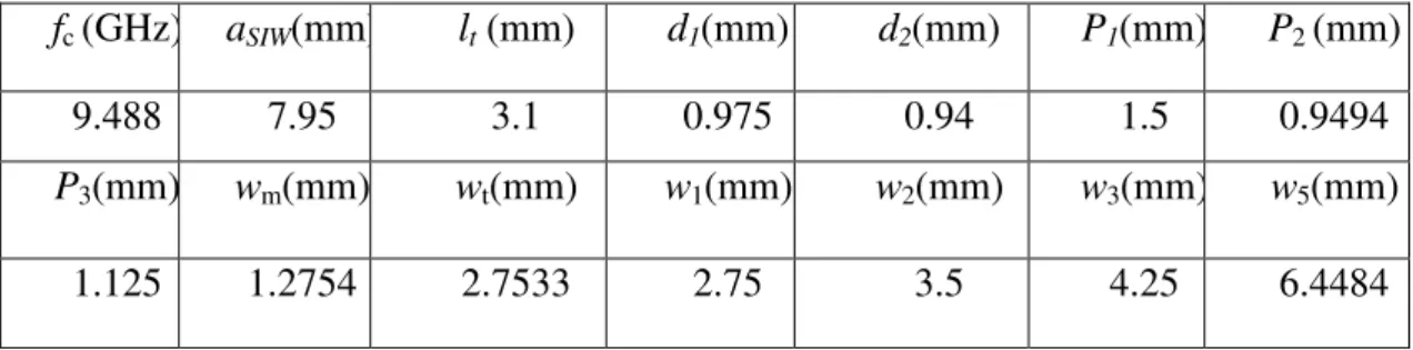
(a) (b) Table 1: Parameters dimensions for the first structure.
f
c(GHz)
a
SIW(mm)
l
t(mm)
d
1(mm)
d
2(mm)
9.488
9.9502
3.1
0.975
0.97
P
1(mm)
P
2(mm)
P
3(mm)
w
m(mm)
w
t(mm)
1.5
0.9494
1.125
1.2754
2.7533
w
1(mm)
w
2(mm)
w
3(mm)
w
4(mm)
w
5(mm)
2.75
3.5
4.25
6.5
8.4486
Fig. 4. S-parameters of the Transition micorstiop to SIW. (a) Transmission coefficients ; (b) Reflection coefficients
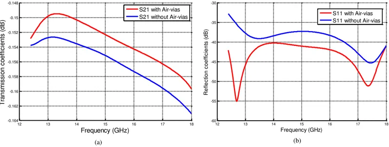
In the second structure, some parameters have changed and presented in the table.2. Two holes from
both sides of the microstrip that have a distance
w
4 between them were removed, (Fig.2.c) and thesubstrate is chosen as Rogers RO3003 with εr=3. Fig. 5 shows the comparison between the simulated
S parameters of the proposed transition and the taper-via transition in Ku-band frequency. From Fig.
5(a), we can see that the insertion loss is lower than 0.17 dB for taper-via transition and lower than
0.16 for the proposed transition. in Fig. 5(b), the return loss is higher than 33 dB for taper-via
transition, and higher than 40 dB for the proposed air-via transition.
Table 2: Parameters dimensions for the second structure
f
c(GHz)
a
SIW(mm)
l
t(mm)
d
1(mm)
d
2(mm)
P
1(mm)
P
2(mm)
9.488
7.95
3.1
0.975
0.94
1.5
0.9494
P
3(mm)
w
m(mm)
w
t(mm)
w
1(mm)
w
2(mm)
w
3(mm)
w
5(mm)
1.125
1.2754
2.7533
2.75
3.5
4.25
6.4484
12 13 14 15 16 17 18 -0.154 -0.152 -0.15 -0.148 -0.146 -0.144 -0.142 -0.14 -0.138 -0.136 Frequency (GHz) T ra n sm issi o n co e ff ici e n ts (d B )
S21 with Air-vias S21 without Air-vias
12 13 14 15 16 17 18 -52 -50 -48 -46 -44 -42 -40 -38 -36 -34 Frequency (GHz) R e fl e ct io n co e ff ici e n ts (d B )
Fig. 5. S-parameters of the Transition micorstiop to SIW. (a)Transmission coefficients ; (b) Reflection coefficients
Fig. 6. Reflection coefficients of back-to-back transition micorstiop to SIW for the second example
In this structure, back-to-back transition is simulated for conventional taper-via and taper with air-vias.
Fig. 6 presents the comparison between the simulated S parameters of the two transitions. We can see that
the return loss is higher than 31 dB for taper-via transition, and higher than 35 dB for the proposed air-via
transition, in the entire Ku-band (12.4 –18 GHz).
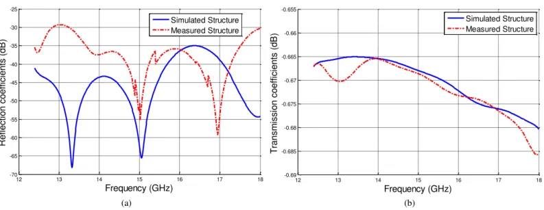
In order to validate the simulated results, an experimental prototype of the proposed back-to-back
transition with air-vias was fabricated (Fig. 7), where the substrate made of RT/duroid 6002 and the
parameters used are presented in table 1. Because of drill size restrictions, the simulation via diameter (cf.
Table 1) was changed for d1 and d2 to 0.95 mm. Fig. 8 presents the comparison between the simulated and
measured results of the new transition with not metalized air-vias and we can see that the simulation
results are in good agreement with the measurements. From Fig.8 (a), in the Ku-band frequency (12.4–
18GHz), the proposed transition shows that the return loss is higher than 35 dB for the simulated results
(a) (b)
12 13 14 15 16 17 18 -0.164 -0.162 -0.16 -0.158 -0.156 -0.154 -0.152 -0.15 -0.148 Frequency (GHz) T ra n sm issi o n co e ff ici e n ts (d B )
S21 with Air-vias S21 without Air-vias
12 13 14 15 16 17 18 -60 -55 -50 -45 -40 -35 -30 Frequency (GHz) R e fle c tio n c o e ff ic ie n ts ( d B )
S11 with Air-vias S11 without Air-vias
12 13 14 15 16 17 18 -65 -60 -55 -50 -45 -40 -35 -30 Frequency (GHz) R e fle c tio n c o e ff ic ie n ts ( d B )
and higher than 29 dB for the measured results whereas in Fig.8 (b) the simulated results of the insertion
loss is lower than 0.68 dB and about 0.685 for the measured results.
Fig. 7. The proposed transition prototype
(a) Front side; (b) Back side.
Fig. 8. S parameter of the proposed transition. (a) Reflection coefficients ; (b) Transmission coefficients
V. CONCLUSION
In this letter, a new transition microstrip to substrate integrated waveguide at Ku-band frequency
is proposed and designed. The back-to-back transition has also been fabricated to confirm the
proposed transition. Simulations results show that the return loss values is around 41 dB over
Ku-band frequency. For the experimental prototype of the back-to-back design, the measured
results are in good agreement with the simulation results, and show that the return loss is better
than 35 dB for the simulated results and
higher than29 dB for the measured results in Ku band
frequency. This new transition with air-vias can give a good platform for RF/microwave circuits
and systems development.
ACKNOWLEDGMENT
This work was supported by the laboratory of electromagnetic and telecommunication,
University of Constantine 01, Route Ain El Bey, 25000, Constantine, Algeria.
12 13 14 15 16 17 18 -70 -65 -60 -55 -50 -45 -40 -35 -30 -25 Frequency (GHz) R e fl e ct io n co e ff ici e n ts (d B ) Simulated Structure Measured Structure
12 13 14 15 16 17 18 -0.69 -0.685 -0.68 -0.675 -0.67 -0.665 -0.66 -0.655 Frequency (GHz) T ra n sm issi o n co e ff ici e n ts (d B ) Simulated Structure Measured Structure
(a) (b)
REFERENCES
[1] D. Deslandes, K. Wu, “Integrated microstrip and rectangular waveguide in planar form,” IEEE Microwave and Wireless
Components Letters, VOL. 11, NO. 02, 68–70, 2001.
[2] H. Nam, T.-S. Yun, K.-B. Kim, K.-C. Yoon, J.-C. Lee, “Ku-band transition between microstrip and substrate integrated
waveguide (SIW),” Asia-Pacific Microwave Conference Proceedings (APMC), VOL. 1, 1–4, 2005.
[3] T. H. Yang, C. F. Chen, T. Y. Huang, C. L. Wang, R. B. Wu, “A 60GHz LTCC transition between microstrip line and
substrate integrated waveguide,” Asia-Pacific Microwave Conference Proceedings (APMC), VOL. 1, 4–7, 2005.
[4] Y. Ding, K. Wu, “Substrate integrated waveguide-to-microstrip transition in multilayer substrate,” IEEE Transactions on
Microwave Theory and Techniques, VOL. 55, NO. 12, 2839–2844, 2007.
[5] Z. Sotoodeh, B. Biglarbegian, F. H. Kashani, H. Ameri, “A novel bandpass waveguide filter structure on SIW technology,”
Progress In Electromagnetics Research Letters, PIER., 2, 141–148, 2008.
[6] F. Bauer, W. Menzel, “A wideband transition from substrate integrated waveguide to differential microstrip lines in
multilayer substrates,” 40th European Microwave Conference (EuMC), 811–813, 2010.
[7] D.-K. Cho, H.-Y. Lee, “A new broadband microstrip-to-SIW transition using parallel HMSIW,” Journal of Electromagnetic
Engineering And Science, VOL. 12, NO. 2, 171–175, 2012.
[8] E. D. Caballero, A. B. Martinez, H. E. Gonzalez, O. M. Belda, V. B. Esbert, “A novel transition from microstrip to a
substrate integrated waveguide with higher characteristic impedance,” IEEE MTT-S International Microwave Symposium
Digest (IMS), 1–4, 2013.
[9] Z. Kordiboroujeni and J. Bornemann, “New wideband transition from microstrip line to substrate integrated waveguide,” IEEE Transactions on Microwave Theory and Techniques, VOL. 62, NO.12, 2983-2989, 2014.
[10] D. M. Pozar, “Microwave Engineering,” 3rd Ed. John Wiley & Sons, 2011.
[11] D. Deslandes, “Design equations for tapered microstrip-to-Substrate Integrated Waveguide transitions,” IEEE MTT-S International Microwave Symposium Digest, 704-707, 2010.
[12]Z. Kordiboroujeni and J. Bornemann, “Designing the width of substrate integrated waveguide structures,” IEEE Microwave