Brazilian Journal of Physics, vol. 29, no. 4, December, 1999 707
High Magnetic Field Transport and Photoluminescence
in Doped InGaAs/InP Superlattices
A.B.Henriques, L.K.Hanamoto, R.F.Oliveira
Instituto de Fsica, Universidade de S~ao Paulo, Caixa Postal 66318, 05315-970 S~ao Paulo, Brazil
P.L. Souza, L.C.D. Goncalves, and B. Yavich
Centro de Estudos em Telecomunicac~oes, Pontifcia Universidade Catolica, 22453-900 Rio de Janeiro, Brazil
Received February 6, 1999 Lattice-matched InP/InxGa1,xAs short period superlattices (
x= 0:53)-doped with Si in the
mid-dle of the InP barriers were studied. The samples had a high carrier concentration which lled two minibands. In addition to a peak associated with the electrons from the second miniband, E2, the
Shubnikov-de Haas spectra showed a well resolved doublet structure that is assigned toE1 electrons
of superlattice wave vectors k
z = 0 and k
z =
=d. From the lineshape of the Shubnikov-de Haas
oscillations, anE1 quantum mobility of 970 cm
2/Vs was deduced, which represents an increase of
about 40% over the value for periodically delta-doped semiconductors. The photoluminescence ex-hibits a band at photon energies higher than the InGaAs bandgap and whose FWHM approximates the Fermi energy of the conned carriers. Thus the photoluminescence observed is consistent with the recombination of electrons conned by the superlattice potential and photoexcited holes.
I Introduction
In doped superlattices electrons are conned by a pe-riodic potential in one dimension which splits the con-tinuous conduction band into a set of discrete energy minibands. By changing the thickness of the compo-nent layers and the doping density, the energy spectrum of carriers can be tuned within a wide range. This char-acteristic makes doped superlattices a unique system in which to study the physical properties of an electronic system with a dimension between 2 and 3, whereby such interesting eects as negative dierential resistance [1] and chaotic transport [2, 3] can be observed.
In addition to the lineshape of the periodic poten-tial and the density of conned carriers, the lifetime of the single-particle states is also a key factor in de-termining the electronic properties of the superlattice. Our previous work on periodically delta-doped super-lattices [4, 5] has shown that the lifetime of the elec-tronic state at the Fermi energy increases with the av-erage distance between the electron spatial distribution and the ionised impurity sheet. In this work we at-tempted to reduce the rate of scattering by increasing
the distance between electrons and impurities. Results obtained on doped InP/InGaAs superlattices are pre-sented. The doping sheet of Si atoms was placed in the InP barriers. In such a structure electrons are re-pelled by the InP barriers, and this repulsion favours their spatial separation from the impurity atoms, which leads to longer single-particle lifetimes.
II Experimental
The superlattices were grown at 640C by LP-MOVPE
in an AIX200 reactor at 20mbar. On a (100) Fe-doped InP substrate, rst a 800A thick undoped buer layer was grown, followed by a 15 period multiple quantum well structure composed of a 50A thick lattice matched InGaAs quantum well and a 50A thick InP barrier. Finally, a 300A InP cap layer was deposited. A Si delta layer with a sheet carrier concentration equal to 4:510
13cm,2was introduced in the middle of the InP
708 A.B.Henriqueset al.
15 seconds after which the silane ux was halted. The growth of the second half of the barriers was triggered 5 seconds later. The period of the MQW structure was determined by x-ray diractometry. The Shubnikov-de Haas spectrum of the sample was measured at 4.2K in magnetic elds of intensity 0-16 T. PL spectra were measured at 4.2K using a set-up whereby light was con-veyed to and from the sample using optical bres.
III Results
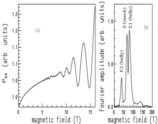
Figure 1(a) shows the Shubnikov-de Haas (SdH) spec-trum of sample 326, and Figure 1(b) shows its Fourier transform. The doublet structure seen in 1(b) at
B80T is due to a resolution of the belly (k
z= 0) and
neck (kz = =d) extremal cross sections of the Fermi
surface associated with the lowest energy miniband E1, whereas the peak at B40T is due to the pocket of
elec-trons conned in minibandE2. Based on the oscillation frequencies observed, the electronic energy spectrum was calculated followingthe same scheme as used previ-ously for periodically delta-doped structures [4]. In the present structures, however, an additional complication arises from the dierence in the eective mass of elec-trons in bulk InGaAs and InP. The miniband energy spectrum was calculated by solving the Schrodinger equation, analogously to the Ben Daniel-Duke proce-dure for quantum wells [6]
c
,
~ 2
2m(z)dzd m(z)1 dz + V (z)d
n(kz;z) = En(kz)n(kz;z) (1)
d
and the Fermi surface was obtained from the equation
~ 2k2
?
2m?(n;kz) + E
n(kz) = EF (2)
where m?(n;kz) is the eective mass associated with
the movement of electrons in a direction perpendicular to the superlattice axis,
1 m?(n;kz) =
Z d=2
,d=2 j
n(kz;z) j
2
m(z) dz (3)
where d is the superlattice period, m(z) is the elec-tronic eective mass in the bulk of the semiconductor material at the position z along the growth axis, and n(kz;z) is the electronic wave function. The
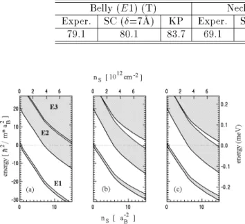
conn-ing potential, V(z), was approximated either by the Kronig-Penney (KP) form, assuming an InP/InGaAs conduction band oset of 230 meV, or obtained from a full self-consistent (SC) solution of equation (1) and the Poisson equation, including the exchange and correla-tion correccorrela-tion in the local density approximacorrela-tion. In the latter case the ionised Si atoms were assumed to be obey a gaussian distribution with a full width at half-height of = 0:05aB (7A for InGaAs) or = 0:21aB
(30A for InGaAs). A comparison of the results of these calculations is shown in Figure 2. This gure shows that the energy separation between the Fermi level and the bottom of miniband E1, (E1) obtained from the KP
and the SC calculations agree within 10% if the den-sity of carriers is less than nS= 10a
,2 B (5:2
10 12cm,2
per superlattice period. However, the same does not hold in the case of excited minibands. For instance, for nS = 8a
,2 B (4:1
10
12cm,2for InGaAs) the SC
calcu-lations with = 0:05aB gives E2 which is more than
2 times greater than the value obtained from the KP model; this ratio falls to 1.8 if = 0:21aB is assumed.
Notice that the disagreement between the KP and the SC models is reduced for a larger , which is because the KP potential approximates better the Hartree SC po-tential for a homogeneous distribution of doping atoms.
Brazilian Journal of Physics, vol. 29, no. 4, December, 1999 709 Table I shows a comparison between the
experi-mental SdH frequencies and the theoretical ones de-duced from the KP and SC approximations, assuming nS = 3:9
10
12cm,2. This value of n
S was chosen
because it gives theoretical SdH frequencies which ap-proximate best the experimental values for miniband E1 - for = 0:05aB, the dierence between theory
and experiment is less than 2%. However, a discrep-ancy remains in respect to the oscillations associated
with E2 electrons, which worsens if increases. This discrepancy is probably due to the eects of residual background doping, non-abruptness of the interfaces and uctuations in the alloy composition, character-istics which were not taken into account in the theory. Our reasoning is based on the observation that the E2 miniband parameters are much more sensitive to the details of the structure than the E1 ones, as Figure 2 demonstrates.
Table I. Experimental and theoretical SdH frequencies for sample No.326. The theoretical values were obtained assuming d=100A and nS = 3:9
10
12cm,2.
Belly (E1) (T) Neck (E1) (T) Belly (E2) (T)
Exper. SC (=7A) KP Exper. SC (=7A) KP Exper. SC (=7A) KP
79.1 80.1 83.7 69.1 68.3 69.6 38.7 21.9 7.2
Figure 2. Energy miniband structure for a InGaAs/InP su-perlattice with period d= 100A (InP and InGaAs layers of
equal width). The Fermi level denes the zero of energy. (a) Kronig-Penney model (b) Self-consistent model with=7A
(c) Self consistent model with=30A.
Assuming nS = 3:9 10
12cm,2 and =7A the
eective mass m?(E1;kz) was deduced from Eq. (3),
and it changed from 0.051m0 at kz = 0 to 0.049m0
at kz = =d. The nearly constant value of m? allows
us to assume that the E1 SdH oscillations will be well described by the tight-binding model [7],
xx
0
,2 X
sinhX exp,uJ
0(u)cos(!u) (4)
where X = 22k BT=
~!
c, !c is the in-plane cyclotron
frequency, = =Q, Q is the quantum mobility in
the E1 miniband, = m?=
~e, is the width of
the miniband, ! = 2m?(E1
,=2)=~e, and J 0 is
the Bessel function of zero order. We have isolated the E1 oscillations from the rest of the SdH spectrum using Fourier techniques. The SdH oscillations so ob-tained were tted using equation (4) to output the
quantum mobility Q. The values of the E1
param-eters and E1 were allowed to evolve from the
ini-tial values output by the SC calculation. As shown in Fig.3, the theoretical curve is in excellent agreement with the experimental one if the quantum mobility is set at Q = 970cm
2/Vs. The quantum mobility for
a delta-doping of the same period (0.72aB) and same
carrier density (7.5a,2
B ) is less than 0.25ea 2 B=
~[8], i.e.
700 cm2/Vs for InGaAs. Thus, by separating the
elec-trons and impurities, an improvement of nearly 40% in quantum mobility was achieved.
Figure 3. Isolated SdH oscillations due to electrons in mini-bandE1 and theoretical result by use of Eq.(4).
710 A.B.Henriqueset al.
the InGaAs bandgap of 0.81 eV, and the width of the luminescence band is about 150 meV, which approx-imates quite well the value of the E1 Fermi energy,
E1
190meV, as deduced from the SC calculations.
This is supportive of associating the observed lumines-cence with a recombination of photoexcited holes and the Fermi sea of electrons conned by the superlattice potential.
Figure 4. Photoluminescence of the InGaAs superlattice at 4.2K.
IV Summary
Doped InP/InGaAs superlattices were studied. Mod-elling of the structures showed that the Kronig-Penney approximation describes with acceptable accuracy the
ground-state electronic miniband, but not the excited ones. Shubnikov-de Haas spectra of the samples showed a very well resolved doublet structure associated with the belly and neck orbits in the E1 miniband. The
quantum mobilityfor electrons conned in theE1
mini-band was deduced to be 970 cm2/Vs. This represents
an improvement of nearly 40% in comparison with pe-riodically delta-doped structures. The photolumines-cence spectrum showed an emission band which is con-sistent with the recombination of photoexcited holes and electrons conned by the superlattice potential.
Acknowledgements
This work was supported by FAPESP, CNPq, and CAPES - Brazilian funding agencies.
References
[1] E. Schomburget al, Phys. Rev. B58, 4035 (1998).
[2] K.J. Luo, H.T. Grahn, K.H. Ploog and L.L. Bonilla, Phys. Rev. Lett.81, 1290 (1998).
[3] F.W. Sheard,Proceedings of the the 24th International Conference on the Physics of Semiconductors (to be published).
[4] A.B. Henriques, L.C.D. Goncalves, N.F. Oliveira, Jr., P.L. Souza & B. Yavich, Phys. Rev. B55, 13072 (1997).
[5] A.B. Henriques, L.C.D. Goncalves, N.F. Oliveira, Jr., S.M. Shibli, P.L. Souza & B. Yavich, Zeitschrift fur Physik B104, 457 (1997).
[6] G.Bastard, Wave mechanics applied to semiconductor heterostructures(Les Editions de Physique, Les Ulis, 1988), p.73.
[7] A.B. Henriques, Phys. Rev. B50, 8658 (1994).